Note : Les descriptions sont présentées dans la langue officielle dans laquelle elles ont été soumises.
~,0.~93~12474 2 1 % 5 6 9 6 PCT/US92/10~06
TTME_DELAY BEAM FORMATION
BACKGROUND OF THE INVENTION
1. Field of the Invention:
The present invention relates to a system for
generating and rapidly changing the time delays of
electrical signals for true ti~e delay beam formation
and steering.
2. Description of Related Art:
The use of wide aperture, wide bandwidth phase
steered array antennas for transmitting and receiving
wideband signals is a known technique. Such known
antennas suffer from a problem of beam dispersion or
broadening when steering away from the array normal.
Attemp~s have been made to avoid this problem of
beam dispersion through the use of time delays
between the array elements. One approach for
implementing true time delay beam form~tion is to
swit~h in different :lengths vf signal transmission
delay lines between the common signal source and the
antenna array elements. This known approach tends to
be bulky and;cumbersome for scanning an array with a
large number of::àrray elements over a wide range of
nearly continuous angles.
It is an:object of he present invention to
provide a system~that is simple and that does not
require a bulky~and co~plex implementationO ~
It is a urther ob]ect of the present invention
to provide a~system for i~plementing true time delay
beam formation~that: may `fit into a ~mall lightweight
package, that lS ~relatively rugged, and that consumes
relatively small amounts of power.
~ ~ .
WO93/1247~ 2 1 2 5 6 9 6 2 PCT/~S92/1~806
SUMMARY OF THE INVENTION:
In accordance with the present invention, these
and other objectives are achie~ed by providing a
system in which time delays may be generated by using
an acousto-~ptic (AO) Bragg cell as a continuous
tapped delay line. Selected points in the Bragg cell
may be optically mapped to the output. The optical
mapping may be controlled using additional optical
and acousto-optical devices. The optical mapping may
make use of prisms and/or holographic optical A
elements, in addition to other standard passive
optical elements.
A system in accordance with the present
invention is capable of gen~rating and rapidly
changing time delays for true time delay beam
formation and steering. A system in accordance with
the present invention enables a time delay beam
formation array to simultaneously scan multiple beams
rapidly over a continuum of angles.
A system in accordance with the present
invention may be used, for example, in airborne
reconnai~sance and surveillance, space-based radar,
satellite communications, or large space-based
arrays, where`size, w~ight and power are major
consideratiQnsO
A system in~accordance with the present
inven ion does not require a bulky and complex
implementation. The hardware required to implement a
true kime delay beam formation system in accordance
with the present invention may fit into a small
lightweight package, may be rugged, and may consume
relatively small amounts of power. The simplicity
and compactness of the system dramatically reduces 7
unwanted variability in the relativ~ time delays~
W~93/12474 ~, ~CT/USg2/~0806 ~
3 21~96
BRIEF DESCRIPTION OF THE DRAWINGS:
A detailed description of a preferred embodiment
of the present invention will be made with re~erence
to the accompanying drawings.
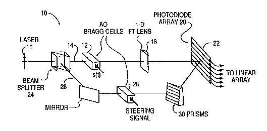
Figur,e l shows an example of an acousto-optic
system for generating a time delay for a one-
dimensional transmitting array.
Figure 2 shows an example of an acousto-optic
system for generating a signal time delay.
Fig~re 3 shows an example of a reference wave on
a photodiode.
Figure 4 shows an example of an ~cousto-optic
system for generating a time delay for a two~
dimen~ional transmitting array.
Figure 5 shows an example of an acous~o-optic
system for generating a time delay for a one-
dimens}onal receiving array.
:
: :
:~ .
:
~ :
`~
W~ 93/1~74 2 1 2 ~ 6 9-6; ~ ; 4 PCl'/US92/1~806
I:~ETAILED DESCRIPTION OF THE PREFERRED EMBODIMENTS:
The following detailed description is of the
best presently contemplated mode of carrying out the
invention. This description is not to be kaken in a
limiting sense, but is made merely for the purpose of
illustrating the general principles of the .invention~
The scope of the invention is best defined by the
appended claims.
Figure 1 shows an example of an acousto-optic
system 10 ~or generating time delays for a one-
dimensional transmi~ting array. The skilled artisan
will recognize a resemblance between the system 10
shown in Figure l as a Mach-Zehnder interferometer.
The signal to be transmitted may be represented
by s(t), where the complex amplitude of the signal s
is a function of time t. ~The signal s(t) drives an
acou~to-optic Br~gg cell 12 located in a first leg 14
of the interferometer system 10. Coherent light from
a laser source 16 may be passed through the Bragg
~0 cell 12 and may be modula ed by the signal s(t~.
A Fourier transform lens 18 may also be provided
in the first l.eg 14 of the interferometer system 10.
Light that is passed through the Fourier transform
lens 18 is separated into a spec rum. Modulated
light exiting from the Bragg cell 12 may be passed
through the Fourier trans~orm~lens 18, thereby
: causing the spectrum~:of the modulated light signal to
illuminate an array Z0 of wideband photodiodes 22.
: ~In the system illustrated in Figure 1, the photodiode
array 20 lS prefera~bly located ln the Fourier
transform plane of the first Bragg cell 12.
Each of the photodiodes 22 in the photodiode
array 20 i5 preferably narrower in one dimension and
wider in another dimension. As shown in ~igure 1,
for example, each of the photodiodes 22 is narrower
in the vertical dimension and wider in the horizontal
WQ93~12474 PCr/~S92/10806
5 ~12~69S
dimension. The width of each photodiode 22 is
preferably large enough to capture the full spectrum
of the modulated light signal illuminating the
photodiode.
The interferometer system 10 illustrated in
Figure 1 also includes a beam splitter 24. The beam
splitter 24 splits the coherent light from the laser
source 16 into a first leg 14 and a second leg 26.
The second leg 26 includes a second Bragg cell
28. A beam steering signal may be inserted into the
second Bragg cell 28. For a single beam, the beam
steering signal may be in the form of a sine wave.
For forming and steering multiple beams, multiple
sine waves may be used. The second leg 26 of
the interferometer system 10 may also be provided
with a stack of prism~ 30. The stack of prisms 30
performs the function of creating, from the output of
: the second Bragg cell 28, a set of plane reference
waves having a range of orientations required to
generate a desired range of time delays.
: More specifically~ the prism stack 30 performs
the function of taking an input beam from the second
Bragg cell 28 at incidence angle ~' and producing
multiple outpût ~beams at angles ~ proportional to ~'.
25: ~ For example, if the~input an~le is fl', then the
: output anyles:would be a~'~k, b~'+k, c~'+k, etc. The
prism stack~30:thereby~performs the function of
~mapping a single angle into multiple angles. The
difference between ~uccessive output angles of the
prism stack 30 is a:function of the input angle ~'~
~hereby producing variable differential time delays.
: ~ Alternatively, the prism stack 30 may be
replaced by a holographic OptlC element. Such a
holographic optic element would similarly perform the
function of creatiny, from the output of the second
WO93/12474 :.~ PCr/US92/108~6
21251~96 6
Bragg cell 28, a set of plane reference waves having
a range of orientations required to generate a
desired range of time delays. In the two dimensional
system shown in Figure 4, for example, the volume
hologram 150 performs substantially the same function
as the prism stack 30 in the one-dimensional system
shown in Figure l. Prisms or volume hologram
elements may be used for beam formation irl antennas
having array elements arranged linearly, as well as
antennas having array elements lying along a curve.
Referring to Figure l, the optics in the second
leg 26 are preferably arranged so that there i5 a
one-to-one correspondence between the photodiodes 22
of the photodiode array 20 and the prisms of the
prism stack 30, whereby each photodiode 22 in the
photodiode array 20 is illuminated by a reference
plane wave output of a corresponding prism of the
prism stack 30.
The interferometer sy~tem lO illustrated in
Figure l is arranged so that the signal spectrum
associated with the f~irst leg 14 and the reference
plane wave associated with the second leg 26
interfere at the~photodiode array 20. Each of the
photodiodes 22 detects the interference between the
signal spectrum and the reference plane wave. Each
of the photodiode~ 22 produces an output signal that
corresponds~to~the detected inte~ference, inteyrated
over the widkh of the photodiode. Since the width of
each photodiode 22 lS preferably large enough to
capture the~ful1 signal spectrum, the integration
- occurs over the fu1l spectral freguency.
The output signal of each of the photodiodes 22
corresponds to a delayed replica of the input signal.
The amount of the delay is determined by the angle
between the reference plane wave and the surface of
the photodiode 22. The output of the photodiode
W~.~3/12474 J
array 20 may be sent to a linear transmitting array
(not shown~. In a preferred embodiment, there is a
one-to-one correspondence between each photodiode 22
of the photodiode array 20 and each element of the
transmitting array.
The following paragraphs provide a mathematical
description of how a system such as that shown in
Fîgure l may generate variable time delays.
As shown in Figures 2 and 3, a reference plane
wave makes an angle ~ with the surface of a
photodiode 22. The reference plane wave at the
surface of the photodiode 22 may be represented
mathematically by:
r ~ t y) e j21~fnt~ YSinO j2~ f"~t-ysina~
where y represents the physic~l distance along the
photodiode 22, ~ represents the optical wavelengkh of
the reference pla~e wave, fO represents the optical
carrier frequency of the reference plane wave, and c
represents the velocity of light. The spectral
frequency f of the signal in the Fourier transform
plane is proportional to the physical distance y
along the photodiode 22. Therefore, a factor f,
hav1ng units of time, may be def1ned such that:
fl= - fOYsin~ ~2~
As indicated in Equation;(2), the factor ~ is
proportional to sin(~). The referenc~ plane wave at
the photodiode may therefore be expressed as,
~(t,f) = ej2~f~ej2~fot ( )
In the first leg 14 of the interferometer system
lO, a coherent optical beam, modulated and Doppler
shifted by the frequency component S(f) of the
WO 93/12474 PCT/US92/10806
signal, also illuminates the photodiode 22. At the
photodiode 22 this modulated coherent beam has the
following functional form:
S(f) ? ej2.pi. ftej2.pi. f0t (4)
The oscillators,
ej2.pi. ft (5)
result from the fact that each frequency component of
the signal in the first Bragg cell 12 Doppler shifts
the optical carrier by the frequency of that
component.
To negate the Doppler shift o fthe steering
signal, a point modulator may be placed in the second
leg 26 of the interferometer system to downshift the
frequency of the optical beam by the frequency of the
steering signal. This Doppler shift could also be
removed electrically at the photodiode output.
The sum of the beams illuminating the photodiode
may be square-law detected using the photodiode. The
output d(t) of the photodiode at each instant of time
is equal to the square-law detection integrated along
the length of the photodiode (i.e., integrated with
respect to the frequency f):
d(t) = ??r(t,f) = S(f) ? ej.pi. fte j2.pi. f0t?2df (6a)
= ??ej2.pi. f?ej2.pi. f0t + S(f) ? ej2.pi. ftej2.pi.f0t?2 df (6b)
=??1 +?S(f)?2 + 2 Real (S(f) ej2.pi. f(5-?-]df (6c)
= bias + 2Real[?S(f)ej2.pi.f (t-?)df] (6d)
WO 93/12474 PCT/US92/10806
Consequedntyly, t photodiode output -(t) may be
represented as,
d(t) = bias +2Real [s(t-?)] (7)
As indicated in Equation (7), the photodiode
output d(t) is equal to the input signal s(t) delayed
by a time ?. The delay time ? is proportional to the
sine of the angle of incidence of the reference plane
wave on the photdiode. The bias allows negative and
positive values of the dealyed singal to be
represented.
A physical explanation of how an acousto-optic
system (as shown, for example, in Figures 1, 2, and 30
can produce an output signal that is a dealayed
replica of the input signal, with the amount of the
delay being determined by teh angle of incidence of
the reference plane wave on the photodiode, is as
follows:
Since the photdiode coherently sums all of the
frequency components of the signal s(t), only those
components of the specturm that are in phase with one
another, after being phase shifted by the reference
signal, will leas to a significant output signal
relative to the bias. Since the reference signal is
a plane wave, the component of the signal spectrum,
in optical form, that contributes to an output signal
must also be a plane wave if, after being pahse
shifted by the reference signal, all points on the
photodiode are to be at the same phase. Referring to
Figure 1, for example, components of the optical
signal that contribute to a plane wave in the Fourier
plane (at the photodiode array 20) come from a single
point in the Bragg cell 12. Thus, the reference wave
selects which point in the Bragg cell 12 (a delay
line) is mapped to the output. The angle of the
reference wave determines the delay of the output
WO 93/12474 PCT/Us92/10806
signal relative to the input signal.
The sytem described above relate generally to
systems for genrating a time delay for a one-
dimensional transmitting array. In the above-
described systems, the photodiode array is preferably
located in teh Fourier transform plane of the first
Bragg cell. Time delays may also be generatged by
placing the photodiode array in the image plane of
the first Bragg cell. Placement of the photodiode
array in the image plane of the first Bragg cell is
particularly appropriate for two-dimensonal array
beam formation.
Figure 4 shows an example of a system 110 for
generating time delays of a signal for forming and
steering the beam of a two-dimensional (planar)
array. The skilled artisan will recognize a
resemblance between the system 110 shown in Figure 4
and a Mach-Zehnder interferometer.
In the system 110 illustrated in Figure 4, time
delays may be generated by placing a photodiode array
120 in an image plane of a first Bragg cell 112 and
optically mapping points in the first Bragg cell 112
onto the photodiode array 120. The electrical
outputs of the photodiode array 120 are time delayed
replicas of the singal s(t). These time delayed
replicas of th signal s(t) are then sent to the
elements of the planar array.
IN the system 110 for a two-dimensional
transmittin garray shown in Figure 4, each of the
photodiodes in the photodiode array 120 sees only the
image of a single point in the first Bragg cell 112.
Consequently, both the vertical and horizontal
dimension of each photodiode in the photodiode array
120 are preferably relatively small. In contrast, in
the system 10 for a one-dimensional transmitting
array shown in Figure 1, the photodiode array 20 is
WO 93/12474 PCT/US92/10806
11
preferably located in the Fourier transform plane of
the first Bragg cell 12. The width of each
photodiode 22 in the photodiode array 20 is
preferably large enough in the horizontal dimension
to capture the full sepectrum of the modulated light
signal illuminating the photodiode.
As shown in Figure 4, a collimated coherent
laser beam from a laser source 116 is divided into a
first leg 114 and a seocnd leg 126 by a beam splitter
124. The optical bema passing through the second leg
126 provides a reference at the photodiode array 120
for heterodyne detection, so that the volatbges from
the electrical signals out of the photodioe array
120 are proportional to the voltages of the time
delayed replicas of the input signal to the device.
Althought the embodiment illustrated in Figure 4 shows
a reference beam generated by a beam splitter 124, it
is noted that neither the reference beam nor the beam
splitter are required elements of the invention. For
example, a reference beam may be provided bya
separate coherent light source. Alternatively, if
the signal to be delayed is of an on-off modified
type, than no reference beam may be required.
In the first leg 114 the input electrical signal
s(t), the signal to be transmitted by the RF planar
array, drives the first acousto-optic Bragg cell 112.
The result is that the first Bragg cell 112 which is
a delay line contains a time span of the signal, in
acoustic form, form time t-T, to time t, where T3
represents the time aperture of the first Bragg cell
112. The coherent laser beam passing through the
first Bragg cell 112 may be modulated by the signal
and Rourier transformed by a first lens 140. Points
in the first Bragg cell 112 are plane waves at a
second Bragg cell 142 and a third Bragg cell 144.
The angular orientations of the plane waves are
WO 93/12474 PCT/US92/10806
12
determined by the positions of the points in the
first Bragg cell 112.
The mapping of points in the first Bragg cell
112 to the photodiode array 120 is controlled by the
frequencies of a vertical electrical signal v(t) and
a horizontal electrical signal h(t) that drive the
seocnd Bragg cell 142 and the third Bragg cell 144.
Both the vertical signal v(t) and the horizontal
signal h(t) are preferably sine waves. The signal in
the second Bragg cell 142 changes the angular
orientation of the plane waves passing through the
second Bragg cell with respect to vertical. The
signal in the third Bragg cell 144 changes the
angular orientation of the plane waves passing
through the third Bragg cell with respect to
horizontal.
The positions and focal lengths of a second lens
146 and a third lens 148 are such that the volume
hologram 150 is also in the Fourier transform plane
of the first Bragg cell 112, so that points in the
first Bragg cell 112 are plane waves in the volume
hologram. The volume hologram 150 is also
approximately in the image planes of the second Bragg
cell 142 and the third Bragg cell 144. Therefore,
the vertical signal v(t) and the horizontal signal
h(t) control the angular orientation of the plane
waves at the volume hologram 150.
The volume hologram 150 is constructed such that
the plane waves at the volume hologram (points in the
first Bragg cell 112) are mapped into points on the
photodiode array 120. The mapping is determined by
the angular orientation of the plane waves at the
volume hologram 150. The mapping of points in the
first Bragg cell 112 onto the photodiode array 120,
and therefore the steering angle of the planar array,
is controlled by the vertical signal v(t) and the
WO 93/12474 PCT/US92/10806
13
horizontal signal h(t).
A large set of point-to-point mappings may be
required to generate the different time delays
necessary for pointing an RF planar array in a large
number of directions. Referring to Figure 4, for
example, the mapping of points from the first Bragg
cell 112 is not required to be one-to-one for a
planar array. For each orientation of the beam, some
number of points in the Bragg cell 112 may be mapped
to a larger number of photodiodes in the photodiode
array 120.
Figure 5 shows an example of an acousto-optic
system 210 for genrating a time delay for a one-
dimensional receiving array. To form a beam in a
particular direction with a receiving linear RF
array, the outputs of the array elements must be
delayed relative to one another and then summed. The
amount of relative delay between the array elements
may be determined by the spacing between the array
elements and by the angle between the beam and the
normal to the linear array.
The principle of how the system 210 illustrated
in Figure 5 delays a signal is essentially the same
as for the system 10 for a one-dimensional
transmitting array as shown in Figure 1. In a first
leg 214 of the system 210 illustrated in Figure 5 a
multi-channel Bragg cell 212 is used. The number of
channels of the Bragg cell 212 is preferably equal to
the number of antenna elements in the linear array.
An electrical signal from each element of the
receiving array drives a channel of the multi-channel
Bragg cell 212. The signal is a channel of the
multi-channel Bragg cell 212 is optically Fourier
transformed onto a corresponding photodiode 222. As
previously described herein, the electrical output of
the photodiode 222 is a time delayed replica of the
WO 93/12474 PCT/US92/10806
14
electrical signal that drives the corresponding
channel of the multi-channel Bragg cell 212. The
time delay may be determined by the angle between the
reference plane wave from a second leg 226 of the
illustrated system 210 and the face of the photodiode
222.
The second leg 226 of the illustrated system 210
functions substantially identically to the second leg
26 in the system 10 shown in Figure 1 to generate
time delays for transmitting a signal with a one-
dimensional array. A stack of prisms 230 in the
second leg 226 results in reference plane waves
having a distribution of angles incident on the
photodiode array 220. This allows a single channel
Bragg cell 228, preferably driven with sine waves, to
control a range of time delays.
The electrical outputs of the photodiodes 222
may be summed electrically. This sum is the signal
arriving at the linear array from the direction
determined by the frequency of the steering signal
driving the Bragg cell 228 in the second leg 226 of
the illustrated system 210.
The system shown in Figure 5 may also be used
for the formation and steering of beams for two-
dimensional (planar) receiving arrays.
The projection of a pointing direction of a
receiving array is a straight line of the face of the
array. The time delays are all the same on each line
ont eh array that is normal to this projection of the
beam pointing direction. Therefore, to form a beam
with a planar receiving array using the system shown
in Figure 5, the outputs of the array elements that
lie along the lines normal to the projection of the
desired beam pointing direction may first be summed
electrically, one sum for each line. The spacing
between the lines is approximately equal to the
WO 93/12474 PCT/US92/10806
spacing between the antenna array elements that lie
along the projection of the beam pointing direction
onto the face of the antenna. The electrical sums
may then be used to drive the channels of the
channeling AO Bragg cell 212 shown in Figure 5. The
steering signal in this case determines the angle of
the formed beam with respect to the normal to the
face of the array.
The electrical outputs of the antenna array
elements may be phase shifted before summing to
compensate for the small deviations of positions of
the array elements from the lines normal to the
pointing direction.
The presently disclosed embodiments are to be
considered in all respects as illustrative and not
restrictive, the scope of the invention being
indicated by the appended claims, rather than the
foregoing description, and all changes which come
within the meaning and range of equivalency of the
claims are therefore intended to be embraced therein.