Note : Les descriptions sont présentées dans la langue officielle dans laquelle elles ont été soumises.
7 ~ ~ ~
K~lV~K/~'V~ FOR A SRT~TAT- NETWORR OF I/O D~VICES
DESCRIPTION
Technical Field
Applicants' invention relates generally to
electrical control mechanisms and more particularly to a
network of single point input and output devices serially
connected to programmable logic controllers or other types of
microprocessor based devices that performs a number of control
functions.
Backqround Art
Input and output control modules for interfacing
with a programmable logic controller (PLC) that is normally
used to control a number of functions in a manufacturing
operation are well known. In most instances, these control
module assemblies are electrically interconnected in a rack
assembly with the PLC. This assembly is often of necessity
WO93/13633 PCT/US92/11~3
~ S1~ 2-
located on the plant floor at a distance from the machinery
used in the manufacturing operation to prevent physical
abuse from dirt, moisture, or vibration. Since many of the
switches, pilot lights, control relays and so on are
located on the machinery, considerable wiring is required
to connect these devices to the PLC since each device
requires at least two wires between it and its respective
- I/O point.
Remote I/O control modules are available that can be
located in a rack assembly mounted directly on the
machinery. Whereas this will reduce the wiring
requirements, the additional rack assembly will require
adding a power supply and a remote network interface module
(NIM) that could be more costly. These assemblies are
generally bulky and require mounting space that may not be
avallable. Each device will still require a direct
connection to the remote I/O control module.
The host PLC will also require a local NIM
Communications between the local and remote NIMs can become
complicated. Each device has an unique address. There
must be a means for each I/O point to know and set its
address location so that it can decode and select the data
meant for it from the various data packets sent over the
communication link by the PLC. It must also be able to
mark its data with its identity when it is being sent back
to the PLC. With very large systems, response times can
become a problem because of the additional overhead
required just for address decoding. Error detection and
correction also becomes more complex as the number of data
packets becomes greater. Typically these packets generally
include a preamble portion containing the routing
information, the data, and an error detection portion such
as a checksum.
6P 4
- 3 - 00219-780 RDF:jy
It is also well known that the I/O control modules
require frequent replacement when a malfunction occurs. Since
a malfunction of necessity shuts down the machine operation,
replacement must be made in a minimum amount of time. Many I/O
control modules have 16 or more I/O points. Replacing the module
would mean removing and reconnecting at least 32 wires. Adding
or deleting control modules for system changes requires
reconfiguration of the individual points for addressing purposes.
The present invention is provided to solve these and
other problems.
Summary of the Invention
According to this invention, there is provided a
receiver module contained in a microprocessor based device for
receiving a serial data packet from a plurality of I/O repeater
modules connected in series over a synchronous serial
communications network, said receiver module comprising: (A)
a clock pulse input means for synchronizing said receiver module
with said synchronous serial communications network; tB) a
buffer register means, coupled to said synchronous serial
communications network, for storing a part of said received
serial data packet from said network; (C) a first shift register
means, coupled to said buffer register means, for storing said
received serial data packet coupled from said buffer register
means and for converting said serial data packet into separate
parallel data bits, wherein said data bits include a true data
bit and a complement data bit from each of said plurality of I/O
repeater modules, said true data bits for indicating the status
_ - 4 - 00219-780 RDF:jy
of each of said I/O modules and wherein said first shift register
means further includes separate parallel outputs of said true
data bits and of said complement data outputs; (D) a detector
means, coupled to said buffer register means, for decoding an end
byte of said received serial data packet to indicate the end of
said received serial data packet; (E) a second buffer register
means having an input coupled to the parallel true data bit
outputs of said first shift register means, for coupling said
parallel true data bits to a parallel data bus in said
microprocessor based device; (F) a comparator means, coupled to
said separate parallel outputs of said true data bits and of said
complement data outputs of said first shift register, for
comparing each of said true data bits with its said complement
data bit, for determining if said data bits are valid, and for
generating parallel valid data bits if said data bits are valid;
(G) a third buffer register means, coupled to said comparator
means, for receiving said parallel valid data bits, said third
buffer register means having parallel outputs coupled to said
parallel data bus in said microprocessor based device; and (H)
wherein said second buffer register means transfers said true
data bits to said microprocessor based device and said third
buffer register means transfers said valid data bits to said
microprocessor based device.
According to this invention, there is provided a
receiver module contained in a microprocessor based device for
receiving a serial data packet from a plurality of I/O repeater
modules connected in series over a synchronous serial
.s - ,~
7 ~ ~ -
~ - 4a - 00219-780 RDF:jy
communications network, said receiver module comprising: (A)
a clock pulse input for synchronizing said receiver with said
synchronous serial communications network; (B) a buffer register
coupled to said synchronous serial communications network, said
buffer register storing a part of said received serial data
packet from said network; (C) a detector coupled to said buffer
register, said detector decoding a start byte and an end byte of
said received serial data packet, said start byte to indicate the
beginning of said received serial data packet and said end byte
to indicate the end of said received serial data packet; (D)
wherein said start byte and said end byte consist of a series of
different logic levels including at least one logic high and one
logic low; (E) wherein said detector compares said different
logic levels of said start byte and said end byte to determine
if all of said different logic levels are logic highs, indicative
that said synchronous serial communications network is open
circuited; and (F) wherein said detector compares said different
logic levels of said start byte and said end byte to determine
if all of said different logic levels are logic lows, indicative
that said synchronous serial communications network is short
circuited.
Other features and advantages of the invention will be
apparent from the following specification taken in conjunction
with the accompanying drawings in which there is shown a
preferred embodiment of the invention. Reference is made to the
claims for interpreting the full scope of the invention which is
not necessarily represented by such embodiment.
~' ~
~ ~ 7 ~ ~
_ - 4b - 00219-780 RDF:jy
Brief Description of Drawinas
FIG. 1 is a block diagram of a communication system
according to the present invention.
FIG. 2A and 2B is the data format of the data stream
as it progresses through the separate input/output repeater
modules coupled to the network.
FIG. 3 shown various waveforms representative of
different binary representations of data bytes.
FIG. 4 is a block diagram of the transmitter module
located in the programmable controller connected to the network.
FIG. 5 is a block diagram of the receiver module
located in the programmable controller connected to the network.
FIG. 6 is a block diagram of an input/output repeater
module coupled to the network.
/ /
'/
,\
"'O 93/13633 2 I 2 ~ 7 ~ ~ PCT/US92/11253
-5-
Detailed Description
Although this invention is susceptlble tO
embodiments of many different forms, a preferred embodiment
will be described and illustrated in detail herein. The
present disclosure exemplifies the principles of the
invention and is not to be considered a limit to the
broader aspects of the invention to the particular
~ embodiment as described.
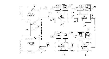
- Referring to FIG. 1 of the drawings, a iow cost
communication system between a programmable logic
controller (PLC)10 and a network of remote lnput/output
repeater (IOR) modules 12 uslng a synchronous
communications protocol is disclosed. The PLC 10 contains
a CPU 14 for executing a ladder program for cor.t~olling a
number of functions in a manufacturing operation. A data
bus 15 connects the CPU 14 with a point I/O transmitter 16
and a point I/O receiver 18. A serial loop communications
network 20 starts with the transmitter 16, interconnects
with each IOR 12, and terminates with the receiver 18. The
transmission medium for the network 20 may be wire or fiber
optical. Input devices 22 and output devices 24 for the
manufacturing operation which respond and interact with the
ladder program are connected to the IORs 12. Each remote
IOR 12 has the capability of providing for an input, an
output, or both. The network 20 is multiconductor and
requires two signal lines, including a serial data line 20a
and a clock line 20b. Additional wires provide power
distribution and ground referencing. The number of remote
IORs 12 on the network 20 is only llmited by the
transmission medium and system parameters such as clock
frequency, cycle times, etc. The address of each remote
IOR 12 is not unique as it is automatically determined by
its position in the loop between the transmitter 16 and the
receiver 18. A serial data packet 21 of information
transmitted over the serial data line 20a consists of an
WO93/13633 ~ PCT/US92/112~3
~ 6
input sync 30, an output sync 31, and data 32-37. The
packet length is dependent on the number of remote IORs 12
connected to the network 20. The input sync 30 and output
sync 31 consists of bit patterns that the IORs decode to
determine when they should extract or add data to the
packet representative of the status of the input and output
devices connected to them. The clock line 20b synchronizes
~the transmitter 16, the IORs 12 and the receiver 18.
As the ladder program is executing in the PLC,
various output devices 24 require either energization or
deenergization. The CP~ will generate data bytes for each
of the output devices 29. These data bytes are coupled to
the point I/O transmitter 16 by the data bus 15. The point
I/O transmitter 16 generates the serial data line 20a which
contains the output data bytes and clock line 20b. The
serial data line 20a, as shown in Fig. 2, as it leaves the
transmitter 16, and as it enters the first IOR 12a at point
26, is in the form of the input byte 30, output byte 31,
and n bytes of output data O(n) in ascending order, where n
is the total number of IORs 12 connected on the network and
n=l is the first device on the network 20 closest to the
transmitter 16. When the serial data packet passes through
IOR 12a, the data stream is modified. After IOR 12a
decodes the input byte 30, it inserts its input data byte
I~l) 35 which represents the state of the inpu~ device 22a.
IOR 12a will then pass the next data bytes until it decodes
the output byte 31. The next byte of data O(l) 32
represents the required state of output device 2~a. IOR
12a will extract this byte from the data stream and will
then energize or deenergize the output device 2~a connected
to it. The remaining data stream will then be passed on
through IOR 12a to IOR 12b at point 38. This data stream
will be the same length as the data stream at point 26
since the byte length of the added input data byte I(l) 35
is the same as the extracted output byte O(l) 32. The
"'~93/13633 2 1 2 5 7 0 4 PCT/~S92/11253
-7-
second IOR 12b will continue this process. It will add its
input device 22b status data I(2) 36 to the data stream
after decoding the input byte 30 and extract its output
device 24b status data 0(2) 33 after decoding the output
byte 31. This procedure continues through all the
remaining remote IORs 12, 1 through n, resulting in the
final modified data stream having the input byte 30, the
~ input data bytes I(l)~through I(n) in descending order, and
the output byte 31 present at input 40 of receiver 18. All
output data bytes O(n) have been extracted. The receiver
18 will decode the received data stream into data bits
representative of the state of each input device 22
connected to the IORs 12 and couple these data bits onto
the data bus 15 for use by the CPU 14.
The serial data packet 21 is digital so that lt has
only two states, logic 1 or logic 0, to maintain the
simplicity of the system. The free running clock line is
shown by Fig. 3 which also illustrates the various
combinations of the serial data packet. A split-phase
binary representation is used for representation of the
data bytes. Two clock cycles are required to represent one
binary bit of information. A logic 1 becomes a logic high
followed by a logic low as shown by 42a. A logic 0 is a
logic low followed by a logic high as shown by 42b. 42c
shows the representation for the binary 0110. Because all
valid data bits are always logic high-low or logic low-high
combinations, the most consecutive logic highs or logic
lows that can occur in sequence is two. Therefore the
input sync 30 and the output sync 31 can be represented by
three or more consecutive logic highs or logic lows without
mistaking them for valid input or output data bytes.
Details of the point I/O transmitter 16 are disclosed
by the block diagram of Fig. 4. The circuit provides two
main functions, the generation of the serial data line 20a
and the clock signal 20b. The clock signal 20b which is
WO 93/13633 ~ 3~ 8- PCT/US92/11?~3
used to synchronize the devices Gn the network 20 can be
free-running or bursted, but minimum latency is achleved by
free-runnlng. Since the operation of the system is
independent of the clock frequency, the system clock 45
produced by the oscillator 49 can be optimized for the
transmission medium, FCC requirements for EMI and RFI
emissions, system noise considerations, and system cycle
~times. Buffer 46 provides the drive for the network clock
signal 20b. A reset signal ~7 from the CPU 14 over the
data bus 15 starts the transmission of the serial data
p-acket 21 over the serial data line. A shift count counter
48 and a count decoder 49 combine to determine the
transmission packet length which is equal to 2n plus the
input byte 30 plus the output byte 31 clock periods, where
n is the number of remote IORs 12. The decoder 49 produces
a shift/load line 50 for the parallel-in serial-out shift
registers 52 and 56 and a load signal for the shift count
counter 48. Data representing the output state of each IOR
12 is generated by the CPU lq and sent to a buffe- register
54 in a parallel format over the data bus 15. Inverters 53
provide an inversion of each data bit to form the split-
phase binary representation that becomes the output byte
for each IOR 12. Since the output packet length is
dependent on the number of IORs 12 on the network, in those
instances where the IOR 12 is not an output, a valid data
output must still be sent over the network as a place
holder for the IOR 12 to insert its input status in the
proper time slot. The output 55 of buffer register 54 goes
to a parallel in-serial out shift register 56. Data 57
from this shift register is clocked into the output shift
register 52 which combines in order, the input sync pulse
30, the output sync pulse 31 and the output data 57 under
control by the shift line 50. The output from this
register 52 is the data out signal 20a as illustrated in
Fig. 2. Since the number of IORs 12 is not fixed and there
"093/13633 2 1 2 ~ 7 0 ~ PCT/~iS92/11253
-
g
are limitations as to the width Gf the data bus 15, the
data inputs from the data bus 15 may be split in groups of
8, 16 or 32 depending on the data structure of the data bus
15, the CPU 14 and the shift register 56. This allows
virtually an unlimited number of IORs 12 to be connected to
the network 20.
The IOR(1) 12a is detailed in Fig. 5. The IORs 12
~ perform a repeater type function and as a result will have
an-inherent delay with the data received and the data
resent over the serial data line 20a. Minimum system delay
or latency through the IOR is achieved by keeping the delay
to one half of a clock cycle by inverting the clock signal
20b received from the transmitter 16 by inverter 58 SG that
the output clock signal which goes to IOR(2) 12b is
effectively delayed by that amount. The IOR performs
several functions. It monitors the switch input 22a. This
switch input could be from any type (contacts, limit
switches, push buttons, etc.) that could be isolated, but
has been converted to the logic voltage levels of the IOR.
The status of the input device is inserted into the serial
data packet 21 that is sent to the next IOR in the loo~.
The IOR provides a device output signal 24a that can
activate an output driver to plckup a relay, pilot light or
similar output device. The IOR does not require a
hardwired address, eliminating the need for user setup.
Its address is determined by its position on the
communication network 20.
The status of the input switch is inserted into the
serial data packet 21 after the input sync byte 30. DQ
30 flipflops 65, 66, and 67 form a three stage shift register
and are used to clock in the data bits in synchronization
with the clock signal 20b and provide the means for adding
the input data I(1) to and extracting the output da~a O~1)
from the serial data packet 21. The two bit shift register
~5 68 provides a memory for use in decoding of the received
WO93~13633 ~ ~ PCT/US92/112 3
input data by the input sync detector 62 and output sync
detector 63. When detector 62 decodes three consecutive
logic ones followed by a logic zero, representative of the
input sync byte 30 in the preferred embodiment, it sets
latch 60. The output 61 of latch 60 controls the logic
switches 69, 70, and 71. These switches allow the DQ FF 67
to output either the serial data packet 21 directly through
~ an input terminal "a"~of switch 71 when the latch is reset
or,- the serial data packet 21 that has been delayed for two
cycles through DQ FFs 65 and 66 through ar~ input terminal
"b" of switch 71 when the latch is set.
When detector 62 decodes the input sync byte 30 in
the preferred embodiment, it sets latch 60. This makes
input termlnal "b" of switches 69-71 active. At that
instant, DQ FF 66 has stored the status of input switch 22a
and DQ FF 66 has stored the status of the negation of input
switch 22a. These bits will be inserted into the data
stream 22a during the next two clock cycles. The data
stream 22a wlll continue to be sent as received at input
terminal "b" of switch 69 until the detector 63 decodes
three consecutive logic zeros followed by a logic one,
representative of the output sync byte 31 in the preferred
embodiment. Detector 63 will then reset latch 60. This
makes input terminal "a" of switches 69-71 active. At that
instant, the bits in DQ FF 65 and DQ FF 66 will be removed
from the serial data packet 21 and DQ FF 67 will again
output the serial data packet 21 directly through input
terminal "a" of switch 71. The information in DQ FFs 65
and 66 contains the status of the output device 24a at that
instant in time. Exclusive or 72 verifies that the
information is valid and and gate 74 is enabled by the
detector 63 to allow the output status to be determined.
The digital filter/debounce circuit 76 and the output FF 78
provides protection against contact bounce, erroneous data
or noise. The circuit Can be set for changing only if
W093/13633 ~ 4 PCT/~'S92/lt253
1 1
there are three consecutlve periods of equal requests, for
instance. The output of F~ 78 could be used to drive a
triac or other similar device for actlvating an output
device 24a.
The serial data packet 21 has now been modified by
inserting the lnput switch status bits after the input sync
byte 30 and by removing the output switch status bits after
-the output sync byte ~1. The length of the data stream
packet has not changed. In those instances where the IOR
1~ functions only as an input device, the transmitter 16
still must include a valid output data byte for the IOR as
a place holder. Likewise, if the IOR 12 functions only as
an output device, it will insert a valid input data byte
onto the data stream packet, even though the receiver 18
will ignore it. The output of the IOR will be sent to the
next IOR connected in series with it, or in the case of the
last IOR on the network, it will be sent to the recelver 18
for decoding of the input data bytes. A block diagram of
the receiver is presented in Fig. 6, the details of which
follows.
The receiver 18 functions as a shift register and an
error detector. The clock input 20b comes from the last
IOR 12 on the network 20 and is used to decode the input
information that is been inserted into the received serial
data packet 21 by the IORs 12 on the network. The serial
data packet 21 as received at 40 will be in the form of the
4 bit input sync 30, n input data bytes where n is the
number of IORs on the network, and the 4 bit output sync
byte 31.
The 4 bit sync shift register 80 will strip the
input sync byte 30 from the serial data packet 21 by
allowing the serial data packet 21 to be passed through its
registers until the output sync byte 31 is detected. The
resultant data stream 81 will be coupled to receiver shift
register 82 which is a serial to parallel converter. The
WO93/13633 ~ PCT/~iS92/11~53
~s~Q~ ~ 12-
parallel outputs 83 contain the separated spllt phase
representations of each IOR's input data byte. Thus output
83a will be the first bit of the input data byte, which
contains the true status of input device 22a, and output
83b will be the negation of the output 83a. Output 83a,
along with the other IORs' first bit of the input data
bytes, is transferred to data receive buffer register 84.
- Outputs 83a and 83b a~e compared by exclusive "ors" 86.
Since these outputs must always be logically opposite, the
oùtput 87 must always be a logic one. These outputs are
stored in registers 88 which provides a means for detecting
errors by position of the IORs in the received serial data
packet 21. These errors could have been caused by open or
shorted signal lines, noise, or invalid data. Detector 90
monitors the four bit output 91 of sync shift register 80
for the bit pattern of the output sync byte 31. Upon
detection of the pattern, it will signal the buffer
register 84 and the data register 88 that the period has
been completed. Outputs 92 and 94 which contain the status
of the input devices 22 connected to the IORs on the
network will be sent to the data bus 15 for use by the CPU
14 in the execution of its ladder program.
As is the case with the transmitter 16, the number
of input devices 22 is not fixed and there are limitations
as to the width of the data bus 15. The data outputs to
the data bus 15 may be split in groups of 8, 16 or 32
depending on the data structure of the data bus 15, the CPU
14 and the registers 84 and 88. This allows virtually an
unlimited number of IORs 12 to be connected to the network
20.
For minimum latency through the system, the serial
data packets 21 are cyclically free-runnlng with the serial
'~'093/13633 2 1 2 5 7 04 PCT/US92/11253
13-
data line 20a always active with no transmission dead time
or off time. There are no requirements for start or stop
bits, parity bits, checksum bits, or other error checking
codes.
While the specific embodiments have been illustrated
and described, numerous modifications are possible without
departing from the scope or spirit of the invention. The
- IORs can be miniaturi~ed using ASIC packages for direct
integration of the IOR with specific input and output
devices, for example.