Note : Les descriptions sont présentées dans la langue officielle dans laquelle elles ont été soumises.
~ 212696~
PHN 14.497 1 30.03.1994
Capacitive sensor circuit
The invention relates to a capacitive sensor circuit comprising: a sensor
electrode forming a first plate of a sensing capacitor; a first inverting amplifier, having ~ `
an input connected to the sensor electrode and having an output; a second amplifier,
having an input coupled to the output of the first inverting amplifier and having an
5 output; a feedback resistor connected between the output and the input of the first
inverting amplifier. -
Such a sensor circuit is known from European Patent Application No. EP
0,S24,708, where the circuit is used to turn on a personal-care apparatus when it is
lifted by the user of the apparatus and to turn off the apparatus when the apparatus is
10 put down. The sensor electrode, the first inverting amplifier and the feedback resistor
form an oscillator, also referred to as an astable multivibrator, whose oscillation
frequency is dictated inter alia by the value of the feedback resistor and by the
magnitude of the capacitance between the sensor electrode and the signal earth terminal -~
of the capacitive sensor circuit. The oscillation frequency decreases as the capacitance
15 increases. When the user picks up the apparatus the capacitance relative to earth is
comparatively high and the frequency is comparatively low. If the apparatus has been
put down the capacitance relative to earth is comparatively low and the frequency is
comparatively high. The frequency difference or the frequency ratio between the
comparatively low and the comparatively high oscillator frequency is measured by20 means of a frequency-to-voltage converter and is converted into a voltage difference,
which energises a switch to turn on the apparatus. The second amplifier then serves as a
buffer between the oscillating first inverting amplifier and the frequency-to-voltage ~ ' ~
converter. This known capacitive sensor circuit is fairly susceptible to spreads in - ;
properties and values of the components used. It is known, inter a7ia from European -
25 Patent Specification EP 0,104,422, to compare the oscillation frequency with that of a
second oscillator which comprises a reference capacitance relative to earth. Thecapacitance of the sensor electrode is compared with the capacitance of the reference ~ ~ -
capacitor by means of a frequency measurement. A gate circuit provides a signal which ~ ~
- .... :' - '
~ . 2126964
PHN 14.497 2 30.03.1994
is a measure of the oscillation frequencies. This known solution can be accurate but
requires the use of a gate circuit or some other coincidence circuit.
It is an object of the invention to provide a capacitive sensor circuit which
is accurate but does not require such a coincidence circuit, so that it is possible to save
5 components.
To this end, according to the invention, a capacitive sensor circuit of the
type defined in the opening paragraph is characterised in that a series resistor is ~:
connected between the output of the first inverting amplifier and the input of the second ;
amplifier, which series resistor has a resistance value substantially equal to the
10 resistance value of the feedback resistor; a reference capacitor is connected between the
input of the second amplifier and a reference terminal, which reference capacitor has a
capacitance value substantially equal to a predetermined value of the capacitance of the ~ -
capacitive sensor electrode relative to the reference terminal; and in that the first
inverting amplifier and the second amplifier are constructed as Schmitt triggers having -;
15 substantially the same low and high input threshold voltages.
By means of these steps it is achieved that a d.c. Ievel appears on the
output of the second amplifier when the capacitance of the sensor electrode is smaller
than the reference capacitance and that an alternating voltage of the same frequency as ~ ~ ;
the oscillating first inverting amplifier appears on the output of the second amplifier in
20 the opposite case. The change from direct voltage to alternating voltage is hardly
susceptible to tolerances and can be detected reliably by means of a frequency-to-voltage
converter, which converter now merely serves to detect whether a signal is a direct
voltage of zero frequency or an alternating voltage of non-zero frequency. In order to
minimise the influence of component spreads the first-and the second amplifier are
25 preferably identical NAND Schmitt triggers accommodated in one semiconductor body.
The capacitive sensor circuit is suitable for turning on and turning off all
kinds of electrical apparatuses having a handle, such as electric toothbrushes, shavers,
irons, hair driers, drills, vacuum cleaners, and for turning on and turning off electrical
equipment having touch controls, such as audio and video equipment, ovens, cook-tops
30 and the like.
These and other aspects of the invention will now be described and
elucidated with reference to the accompanying drawings, in which
. . .
. .... . i - :
.
:
.. . . ~ ... . -~ :
~-.. . ,. , .. ,.: ~ . - .. :
. ... ~ - .. :
,~ 2l2696~ :'
PHN 14.497 3 30.03.1994
Figure 1 shows a circuit diagram of a capacitive sensor circuit in
accordance with the invention,
Figure 2 shows a circuit diagram of an electrical apparatus comprising a
capacitive sensor circuit in accordance with the invention, and
Figure 3 shows a hair drier having a capacitive sensor circuit in
accordance with the invention built into its handle.
In these Figures parts having the same function or purpose bear the same
reference numerals. -;
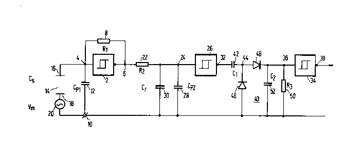
Figure I shows a capacitive sensor circuit in accordance with the
10 invention. A first inverting amplifier 2, in the form of a Schmitt trigger, has its input 4
connected to its output 6 via a feedback resistor 8. Two capacitors are situated between -
the input 4 and a reference terminal 10, which functions as signal earth for the sensor
circuit. A first capacitor is formed by a parasitic input capacitor 12 having a value Cp
and a second capacitor is formed by the capacitance Cs of a sensing capacitor 14,
15 having a first plate formed by a sensor electrode 16 connected to the input 4. The
second plate is formed by the reference terminal 10 which, if desired, may also be
connected to a second sensor electrode 18. For mains-powered apparatuses having a
handle it is adequate to build only the sensor electrode 16 into the handle. The reference
terminal 10 is then coupled to the mains earth Yia the power supply of the sensor : .
20 circuit. The capacitance Cs relative to earth changes when the user takes hold of the
handle. Now it is also possible to detect a hum voltage Vm f mains frequency, which -~
hum voltage is symbolised by an alternating voltage source 20 between the secondsensor electrode 18, if present, and the reference terminal 10. The inverting amplifier 2,
the feedback resistor 8 and the two capacitors 12 and 14 form an oscillator whose
25 oscillation frequency Fs decreases as the overall capacitance Cpl + Cp2 of the .
capacitors 12 and 14 increases. In the afore-mentioned apparatus with a sensor electrode
16 in the handle the oscillation frequency Fs will be comparatively low if the apparatus
is held by the handle and it will be comparatively high if the apparatus is put aside.
When the detected hum voltage Vm is very high there will no longer be a free -
30 oscillation and the oscillation frequency Fs will be pulled to the mains frequency. The
output of the first inverting amplifier 2 is connected to the input 24 of a second -
inverting amplifier 26, also formed by a Schmitt trigger, via a series resistor 22. The
`,. 21269~ .
PHN 14.497 4 30.03.1994
input 24 is connected to the reference terminal 10 via a parasitic capacitor 28 of a value
Cp2 and a reference capacitor 30 of a value Cr.
In order to simplify a rough calculation of the oscillation frequency Fs it
will be assumed, although this is not essential for the operation of the capacitive sensor
S circuit, that the average value of the low threshold voltage Vl and the high threshold
voltage Vh lies halfway the supply voltage V~ and that their difference voltage is Vn:
Vh = 1/2 * (Vcc + Vn); Vl = 1/2 (V~.c - Vn) (1)
.
10 During oscillation the voltage V(t) across the overall capacitance at the input 4 will vary
between the low threshold voltage Vl and the high threshold voltage Vh within one
period T. The voltage across the overall capacitance will vary in accordance with~
V(t) = VO * exp (-t/~) (2)
Here, VO is the initial voltage, ~ = Rl * (CS+Cpl) and Rl is the value of the feedback
resistor 8. When t = Tl2, V(T/2) = Vl and VO = Vh the following will be valid for
one half period: : ~:
20 T/2 = ~ * In {(Vcc + Vn)/(Vcc - Vn)} = ~ ln ~(1+~)/(1 ~Y)}
where c~ = Vn/VcC. For a small value of ~ equation (3) can be reduced to the following ~-
approximation:
T = 4 * T * a~ = 4 * Rl * (Cs+Cpl) * Vn/VcC (4)
The oscillation frequency Fs is therefore approximately equal to:
Fs = Vcc / {4 * Vn * Rl * (Cs + Cpl)}
At the output 6 a squarewave voltage appears which charges and discharges the
capacitors 28 and 30 via the series resistor 22. This results in a ripple voltage across the
capacitors 28 and 30, whose peak-peak voltage Vpp is approximately equal to:
`~ 2l2696~
PHN 14.497 5 30.03.1994
Vpp = Vcc / {4 * Fs * R2 * (Cr + CP2)~ (6)
If R2 is now selected to be equal to Rl and equation (5) is substituted in equation (6) it -
follows that:
Vpp = Vn * (Cs + Cpl) / (Cr + Cp2) ~ -
If now for the second inverting amplifier 26 a Schmitt trigger is used having the same
voltage difference Vn between the high and the low threshold voltage as for the first -~
10 inverting amplifier 2 the following is achieved. Vpp is smaller than Vn if Cs is smaller
than Cr~ so that the two trigger thresholds Vn and Vh f the second inverting amplifier -
26 are not exceeded and a d.c. Ievel appears on the output 32 of this amplifier. Vpp is -
larger than Vn if Cs is larger than Crl so that the two trigger thresholds Vn and Vh are ~-~
exceeded periodically and an a.c. signal with the oscillation frequency Fs appears on the
15 output 32. The voltage difference Vn is substantially equal for the inverting amplifiers 2
and 26 if the amplifiers are identical and are integrated on one semiconductor body.
This has the additional advantage that the parasitic capacitors Cpl and Cp2 are then also
substantially equal and the influence of these parasitic capacitors on the amplitude of - ~ -
Vpp is eliminated. The resistors 8 and 22 have equal values. A parasitic capacitance
20 parallel to these resistors will then neither have any effect on the ripple voltage Vpp ~ -
because a strictly symmetrical load is seen from the output 6 to reference terminal 10.
Thus, it is achieved that the output 32 supplies an a.c. signal if Cs is
larger than Cr and a d.c. signal if Cs is smaller than Cr, inaccuracies as a result
component spreads being largely eliminated owing to the symmetry of the circuit.25 Detection whether the output 32 carries an a.c. or a d.c. signal is possible by means of
a comparator 34, which is also formed by an inverting Schmitt trigger and which has an
input 36 and an output 38, which input 36 receives a signal from the output 32 of the
second inverting amplifier 26 viu a charge pump 40. The charge pump 40 comprises a
first capacitor 42 connected between the output 32 and a node 44, a first diode 46,
30 having its cathode connected to the node 44 and its anode to the reference terminal 10,
a second diode 48, having its anode connected to the node 44 and its cathode to the
input 36, and a resistor 50 and a capacitor 52, which are connected between the input
36 and the reference terminal 10. ~;
~'','"'
~ 212ggfi~
PHN 14.497 6 30.03.1994
The charging current i through the capacitor 42 per oscillation period l/F
is approximately equal to~
i = Cl * (Vcc - 2*Vj - V2) * F = V2 / R3 (8)
S
In this equation Cl is the value of the capacitor 42, Vj is the junction voltage of the
diodes 46 and 48, V2 is the voltage across the capacitor 52, and R3 is the value of the
resistor 50. If the threshold voltages of the comparator 34 lie approximately halfway the ;~
supply voltage Vcc the voltage V2 must be equal to Vcc/2 at the minimum frequency F
10 and the following equation is valid:
.: ~
Fl = Vcc / ~R3 * Cl * (Vcc - 4 Vj)}
As stated hereinbefore the oscillation frequency may be equal to the detected mains
15 frequency. When Fl = 20 Hz, Vcc = 5 V and Vj = 0.7 V it follows from equation (9)
that the time constant R3*CI has a value of approximately 114 ms. The capacitor 52
provides some delay in the change-over of the comparator 34.
Figure 2 shows the capacitive sensor circuit of Figure 1 used in an .
electrical apparatus. The inverters 2, 26 and 34 are implemented by means of dual input
20 Schmitt trigger NANDs. The output 38 of the inverter 34 drives the base of an NPN
switching transistor 56 via a fourth dual input Schmitt trigger NAND 54 and a current
limiting resistor 74, the emitter of said switching transistor being connected to the
reference terminal 10 via a light-emitting diode (LED) 58 and the collector of this
transistor driving the energising coil 62 of a relay 64 via an interrupter switch 60. The
25 relay and the NANDs receive their supply voltage from a supply voltage source, not
shown, which may comprise a rectifier circuit, not shown. The relay actuates a switch
66, which is arranged in series with a load 72 between mains voltage terminals 68 and
70. The load 72 may be, for example, a motor, a heating element, a lamp or any other
device to be turned on and turned off.
At comparatively low oscillation frequencies, i.e. when the sensor
electrode 16 is approached as in the case that the apparatus is taken hold of, an a.c.
signal appears on the output 32, so that the input 36 is high. The output 38 is then low
and the transistor 56 is turned on via the inverter 54. The energising coil 62 of the relay
~ ~126~
PHN 14.497 7 30.03.1994
64 is energised, the switch 66 is closed and the load 72 receives mains voltage. By
means of the interrupter switch 60 the power supply to the energising coil 62 can be
interrupted to render the electrical apparatus inoperative. The LED 58 signals that the
load is connected to the mains via the switch 66. When the apparatus is put aside the
5 oscillation frequency is comparatively high, the output 32 is then continually high and
the input 36 is low, so that the output 38 is high and the transistor 56 receives no base -
current. Now the relay 64 is not energised, the LED 58 is turned off and the load 72 is
disconnected from the mains voltage. Thus, the relay is energised in response to the -
a.c./d.c. signal on the output 32 of the second inverting amplifier 26.
The second amplifier 26 may alternatively be non-inverting because this is
irrelevant for the decision whether an a.c. signal or a d.c. signal is present on the
output 32. The value Cr of the reference capacitor 30 depends on the envisaged values -~
of the sensing capacitor 14.
Figure 3 shows an electric hair drier having a handle 74, in which the
lS sensor electrode 16 is mounted. The capacitive sensor circuit and the other electronic -
devices of Figure 2 are accommodated on a p.c. board 76, which is also mounted in the ~ -
handle 74.
~ ~' '. ' ' ' ~ '`
~-- ~.::''.
. ~ ~
' .