Note : Les descriptions sont présentées dans la langue officielle dans laquelle elles ont été soumises.
2128743
1
TITLE OF THE INVENTION
AN OPTICAL FILM, AN ANTIREFLECTION FILM, A
REFLECTION FILM, A METHOD FOR FORMING THE OPTICAL FILM,
THE ANTIREFLECTION FILM OR THE REFLECTION FILM AND AN
OPTICAL DEVICE
BACKGROUND OF THE INVENTION
1. Field of the Invention
The invention relates to an optical film and a
method for forming it, and an antireflection film and a
method for forming it, and a reflection film and a method
for forming it, and an optical device having an optical
film.
2. Description of the Related Art
In recent years, optical telecommunication systems
using optical fibers have been made longer in distance,
greater in capacity, and faster in speed, and light has
been used for signal transmission between inte~rated
circuits. In such a manner as this, information
transmission technologies utilizing lightwave been
remarkably developed.
In order to make a greater progress in the
technologies utilizing light, it is necessary to develop
a high-output and stable light source precisely made, a
means~for precisely controlling light, a transmission
path lower in loss, an optical transducer lower in loss,
and the like. A means for precisely controlling light
includes to use various optical films in an optical
transmission path,, an optical transducer, and the like,
and to use an antireflection film, a reflection film, and
the like for composing a resonator of a semiconductor
laser (a laser diode).
An antireflection film used for a semiconductor
optical device is described in the following.
For example, an antireflection film formed on the
optical output end face of a semiconductor laser is
required to be 0.01 0 or less in reflectivity. In an
~I~'874~
2
ordinary technical field of lens coating, a dielectric
film of multi-layered structure comprising 15 layers is
adopted as an antireflection film in order to attain such
reflectivity as this.
In a semiconductor laser also, it is thought to use
such a multi-layered dielectric film as this, but the
same optical film as used in a technical field of lens
coating cannot be applied to the semiconductor laser as
it is, since a material composing the film or a method
for forming the film is one of the determinate factors
controlling life time of the optical semiconductor
device. Since in a semiconductor laser there are
restrictions on material of an antireflection film or a
method for forming the film from a viewpoint of its
composing material or its construction, there is no way
except selecting a material or method on the basis of
experimental facts. And considering difference in
coefficient of thermal expansion between the film hnd the
semiconductor laser, it is desirable to make the number
of layers composing the antireflection film as small as
possible.
The smallest number of layers for obtaining
reflectivity useful for the purpose of an antireflection
film is "2". For example, a film of two-layered
structure comprising optical films of high and, low
refractive indexes is used as an antireflection film
derived from computing an optical propagation constant of
a semiconductor laser of 1.55 pm in wavelength, in which
the optical film ,of high refractive index is 2.44 in ,
refractive index and 1450 A in thickness and the optical
film of low refractive index is 1.37 in refractive index
and 2750 ~ in thickness. The reflectivity obtained by
this antireflection film is kept to be 0.01 ~ or less.
An optical film of 1.37 in refractive index can be
formed by an ordinary vacuum deposition method using such
an optical material as lithium fluoride (LiF) or
magnesium fluoride (MgFz), but an optical material
_2128743
3
composing an optical film of 2.44 in refractive index is
unknown yet. Although zinc selenium (ZnSe) of 2.46 in
refractive index is used as a material having a
refractive index near to 2.44, this material cannot be
greatly changed in refractive index.
A reflection film used in an optical device is
described in the following.
For example, a reflection film for composing a
resonator of a semiconductor laser is required to be low
in loss and comparatively high in reflectivity so as to
match with characteristics of the device.
In a technical field of lens coating or the like
where a wavelength range of visible light is mainly used,
it is known that a high reflectivity of low loss can be
obtained by combining such a high-refractive-index
optical film of 2.0 to 2.4 in refractive-index as zinc
sulfur (ZnS), cerium oxide (CeOz), or zinc selenium
(ZnSe) together with such a low-refractive-index dptical
film of 1.35 to 1.47 in refractive-index as silicon oxide
( Si02 ) , MgF2 , car biF.
However, since wavelength of a laser light is in a
near infrared range in a technical field of a
semiconductor laser made of compound semiconductor of the
III to V groups, two conditions need to be satisfied that
the high-refractive-index optical film has a higher
refractive index than the above-mentioned refractive
index of 2.0 to 2.4 and that the optical films have
little light absorption so as to obtain a high output.
Therefore, the above-mentioned materials of high
refractive index are not optimal. Silicon (Si),
germanium ( Ge ) , and the like are known as a material
satisfying the condition of having a high refractive
index, and for example, there is a high-reflectivity film
of mufti-layered structure in which a pair of Si and Si02
layers are respectively formed in thickness of 1/4
wavelength. Although a reflection film of this
combination is used in a semiconductor laser, it does not
2I2~743
fully satisfy the above-mentioned two conditions, since
Si and Ge have a light absorption band in the near
infrared range.
Although various improvements of crystal growing
methods have been suggested as a method for reducing
light absorption of the Si layer, they have hardly
brought any good result.
For example, a method of growing a silicon film by
means of deposition has a merit that thermal damage is
little given to the semiconductor because of formation of
the film at a low temperature and the film thickness can
be precisely controlled by setting a film thickness gauge
inside the chamber, but on the contrary the method has a
demerit that the silicon film has a great light
absorption since it is polycrystalline.
And although a method of growing a silicon film by
means of CVD can stably make a specified film quality, it
gives some damage to the semiconductor since i't is a
high-temperature process.
Even if in case of using a silicon layer as a high-
refraction-index layer composing a multi-layered
reflection film there is a method of improving its
crystallinity in a low-temperature process, the silicon
interferes with the laser oscillation when it comes in
contact with the p-n junction interface of , the
semiconductor laser since the silicon is higher in
electric conductivity than such dielectric as glass.
As mentioned above, since a semiconductor laser
does not give a designed performance in case that a
specified refractive index cannot be obtained for a high
refractive-index layer to compose a multi-layered
antireflection film or reflection film, a material of an
optical film having a refractive index optimal for
improving its performance or a method for forming such an
optical film is desired.
And an optimal refractive index of an optical film
composing an antireflection film or reflection film to be
222873
used for a semiconductor optical device does not have
only one value, but needs to be changed according to
structure of an optical waveguide of the semiconductor
laser. Therefore, a technique capable of freely adjusting
5 a refractive index of the antireflection film or
reflection film is desired.
SUMMARY OF THE INVENTION
It is an object of the present invention to provide
an optical film having a high-refractive-index layer
whose refractive index is be changed in a wide range
according to its growth conditions and to provide a
method for forming the optical film and an optical device
having the optical film. And other objects of the
invention are to provide an antireflection film having an
optimal high-refractive-index layer and a method for ..
forming the antireflection film and still further to
provide a reflection film having an optimal: high
refractive-index layer and a method for forming the
reflection film.
The present invention makes a high-refractive-index
layer in a multi-layered optical film of titanium oxidic
nitride(TiON) and makes a high-refractive-index layer
composing a multi-layered antireflection film or
reflection film of titanium oxidic nitride. ,
A titanium oxidic nitride film is easily adjusted
in refractive index in a range of 2.2 to 4.0 by properly
choosing conditions~of an ion assist deposition method.
Since i.ts growth. temperature is as low, as a silicon
growth, the growing process does not affect a device
characteristics in case of applying it to a semiconductor
optical device. And the titanium oxidic nitride film is
a dielectric film and so it does not cause electric
current to leak in case that the titanium oxidic nitride
film is formed on a p-n junction interface of the
semiconductor optical device. Furthermore, since the
light absorption by its crystal is less as compared with
,7,.
CA 02128743 1998-12-09
- 6 -
lsilicon and is as slight as ZnSe, attenuation in intensity of
the optical input and output of the optical device is
suppressed.
Therefore, the light emission or light detection by
an optical device results in being precisely controlled by
forming a multilayered optical film having an optimal
refractive index for each of various optical devices.
In accordance with the present invention there is
provided an optical film of multilayered structure comprising
a high-refractive-index layer composed of titanium oxynitride
and a low-refractive-index layer, said optical film being
formed on an optical input/output portion of a semiconductor
laser.
In accordance with the present invention there is
further provided an optical film forming method comprising the
steps of: forming a low-refractive-index layer on an
input/output portion of a semiconductor laser; and forming a
titanium oxynitride layer, by an ion assist deposition method,
on said low-refractive-index layer as a high-refractive-index
layer.
In accordance with the present invention there is
further provided an optical film of multilayered structure
comprising; a high-refractive-index layer and a low-
refractive-index layer; wherein the high-refractive-index
layer is composed of a titanium oxynitride film having a
refractive index in a range of 2.2 to 2.9 for a visible light,
wherein the low-refractive-index layer is composed of one of
28801-2
CA 02128743 1998-12-09
- 6a -
magnesium fluoride and lithium fluoride, and wherein the
multilayered structure is an antireflection film formed on a
substrate.
In accordance with the present invention there is
further provided an antireflection film forming method
comprising: forming a high-refractive-index layer composed of
titanium oxynitride on an optical input/output portion of an
optical device by an ion assist deposition method, and forming
a low-refractive-index layer on the high-refractive-index
layer; wherein the ion assist deposition method is a film
forming method of vaporizing a raw material of the high-
refractive-index layer by irradiating electrons from an
electron gun onto a block of the raw material and irradiating
the vaporized raw material onto an optical input/output
portion and at the same time ionizing a first gaseous element
inside an ion gun and ionizing a second gaseous element
outside the ion gun by the first ionized gaseous element and
bonding the ionized gaseous elements together with the
vaporized raw material.
In accordance with the present invention there is
further provided a reflection film forming method comprising:
forming a low-refractive-index layer on an optical
input/output portion of an optical device; and forming a high-
refractive-index layer composed of titanium oxynitride on the
low-refractive-index layer by an ion assist deposition method,
wherein the ion assist deposition method is a film forming
method of vaporizing titanium oxide as a raw material of the
28801-2
CA 02128743 1998-12-09
- 6b -
high-refractive-index layer by irradiating electrons from an
electron gun onto a block of the raw material, at the same
time ionizing a gaseous element of nitrogen from an ion gun,
and bonding the ionized gaseous element together with the
vaporized raw material.
In accordance with the present invention there is
further provided a semiconductor laser, comprising: a laser
construction having an activated layer held between two clad
layers; a first electrode formed on an upper surface of said
laser construction; a second electrode formed on a bottom
surface of said laser construction; a first high-refractive-
index layer composed of titanium oxynitride formed on one side
of the laser construction; and a first low-refractive-index
layer formed on the first high-refractive-index layer.
In accordance with the present invention there is
further provided an optical film forming method comprising the
steps of: forming a titanium oxynitride layer, by an ion
assist deposition method, as a high-refractive-index layer
onto an input/output portion of a semiconductor laser; and
forming a low-refractive-index layer onto the titanium
oxynitride layer.
BRIEF DESCRIPTION OF THE DRAWINGS
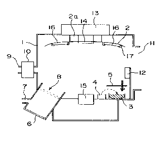
Figure 1 is a structural drawing for showing an
example of an ion assist deposition apparatus used for forming
an optical film of the present invention.
Figure 2 is a characteristic graph showing relation
between a deposition rate and refractive index of a TiON film
28801-2
CA 02128743 1998-12-09
- 6c -
of the present invention formed by means of an ion assist
deposition method.
Figure 3 is a characteristic graph showing relation
between ion current and refractive index of an optical film in
an ion assist deposition method to assist an element composing
an optical film of the present invention.
Figure 4 is a characteristic graph showing relation
between a ratio of oxygen in an oxygen-nitrogen mixed gas and
a refractive index in case of forming an optical film of the
present invention by means of an ion assist deposition method.
Figure 5 is a characteristic graph showing relation
between a deposition rate and refractive index of an optical
film of the present invention formed by means of an ion assist
deposition method introducing nitrogen and oxygen respectively
from intakes different from each other.
Figure 6 is a cross-sectional view of a
semiconductor laser according to an embodiment of the present
invention.
Figure 7 is a graph showing relation between
temperature and a percentage of the accumulated number of
28801-2
2.~28'~43
semiconductor lasers deteriorated in characteristics in
a humidity test in case of applying an optical film of
the present invention and in case of applying an optical
film of the prior art.
Figure 8 is an exterior view showing a
semiconductor optical device according to another
embodiment of the present invention.
Figure 9 is a graph showing relation between
ionizing current and refractive indexes of optical films
respectively in case of ionizing only nitrogen and
applying the ionized nitrogen to a substrate and in case
~of ionizing nitrogen and oxygen and applying the ionized
nitrogen and oxygen to a substrate in an ion assist
deposition method used in forming optical films of the
present invention.
Figure 10 is a cross-sectional view of a
semiconductor laser according to still further another
embodiment of the present invention. ,'
DESCRIPTION OF THE PREFERRED EMBODIMENTS
The present inventors thought using titanium oxidic
nitride ( TiON ) and other oxygen and nitrogen compounds of
dielectric instead of using ZnS, CeOz, ZnSe, Si, Ge, or
the like as a material of high-refractive-index optical
Z5 films composing a multi-layered reflection film or a
multi-layered antireflection film.
And as a method for forming oxidic nitride we used
an ion assist deposition method which keeps low a heating
temperature of the ground layer the TiON is to, be
deposited on, gives a very good adhesion of the TiON film
and the ground layer, and makes it easy to adjust a
refractive index of the TiON film. The ion assist
deposition method is a method for forming a film by
irradiating ions of plural elements onto a substrate.
In case of using the ion assist deposition method
for forming an optical film, two methods for controlling
a refractive-index are thought including ( 1 ) adjusting a
2Z2~743
8
refractive index of an optical film by increasing a
filling degree of the optical film through irradiating
ions of a component element of the optical film onto the
grown optical film and (2) adjusting a refractive index
of an optical film by changing a composition ratio of
elements composing the optical film, where the "filling
degree" shows a degree of the number of holes existing in
atomic unit inside an optical film formed by deposition,
and the larger the filling degree is, the smaller the
number of holes is.
The former method (1) has a more narrow range of
adjusting the refractive index, while the latter method
( 2 ) has a wider range of adjusting the refractive index.
The present inventors found a method of forming an
optical film having a TiON film or other oxygen and
nitrogen compound films by means of an ion assist
deposition method and a method of applying the optical
film to such an optical device as a light defecting
device, a light emitting device, and an optical
modulator, or to such optical parts as optical fiber and
lenses. The methods are described in detail in the
following.
Before description of an optical film according to
the invention, construction of an ion assist deposition
apparatus used for forming the optical film is described
in brief.
Figure 1 is a structural drawing for showing an
overview of an ion assist deposition apparatus used for
forming an optical film of the present invention.
On the ceiling of a deposition chamber 1, a rotary
dome 2 ( substrate supporting plate ) to hold substrates 16
on its downside face so as to be turned by a revolving
part 2a. On one corner of the bottom of the deposition
2.1287~~
9
an electron gun 4 for irradiating electrons onto the raw
material in the crucible 3 of cartridge type is set next
the crucible 3. On another corner of the bottom of the
deposition chamber 1, an ion gun 6 of Kaufmann type
(whose gas discharging outlet is 80 mm in diameter and
1100 mm distant from the center of the rotary dome 2 ) is
set opposite to the substrate supporting face of the
rotary dome 2. This ion gun 6 introduces gas through an
ionizing gas introducing intake 7, ionizes the gas with
thermal electrons from a filament (unshown), and
discharges the ionized gas toward the rotary dome 2 by
some voltage applied to an ion accelerating electrode 8.
A gas introducing intake 9 is formed in the side
wall of the deposition chamber 1 between the ion gun 6
and the rotary dome 2, and a gas introduced through the
gas introducing intake 9 is adjusted in flow by means of
an automatic pressure regulator 10. An exhaust outlet 11
is made in the side wall of the deposition chamber 1
opposite to the gas introducing intake 9 and a deposition
rate monitor 12 of crystal oscillator type is set near to
the exhaust outlet 11 and the shutter 5.
On the upside of the middle part of the rotary dome
2 a first film thickness monitor 13 of photoelectric type
far monitoring film thickness with a reflected light is
provided, which monitors thickness of the film formed on
a glass substrate 14 for monitoring which is set on the
downside face of the middle part of the rotary dome 2.
And opposite to the~first film thickness monitor '13 of
photoelectric type and between the ion .gun 6 and ;the
electron gun 4, a second film thickness monitor 15 of
photoelectric type is provided, which measures thickness
of the film on the surface of the glass substrate 14 for
monitoring on the basis of a light which has transmitted
through the glass substrate 14. A light source of the
transmitted light is inside the first film thickness
monitor 13 of photoelectric type. The reflected light is
0.65 um in wavelength and the transmitted light is 1.55
. ~
'r. ' '. . .. ,
'
. , . . . '-.:' ,. ' ~ , r .:,'
.. . , .,.' . .. -_;; ;:.
. ; :~ ; ~.. ...,..:.
'
~
'
. ~
. . ,
i
,
.
.
21~~7~~
to
um in wavelength.
Reference number 17 shows a holder for holding the
substrate 16 on the downside face of the rotary dome 2.
Film forming methods are described in the
following. First to third embodiments relate to methods
for forming a high-refractive-index layer to compose an
antireflection film, and embodiments following them
relate to methods for forming a high-refractive-index
layer to compose a reflection film.
(First example)
A method for forming an optical film of the first
embodiment by means of the above-mentioned ion assist
deposition apparatus is described in the following.
This embodiment makes a high-refractive-index
optical film of TiON which composes a two-layered
antireflection film to be used in a semiconductar laser
of 1.55 um in wavelength as an example. zt is desired to
control an refractive index of the high-refractive-index
optical film to be in a range of 2.50 to 2.60 to make it
function as an antireflection film far that wavelength.
First, substrates 16 to have an optical film formed
on them are mounted on the downside face of the rotary
dome 2 around the glass substrate 14 for monitoring, and
a crucible 3 of cartridge type filled with Ti3 OS which is
a raw material is set in the deposition chamber 1" and
then gas inside the deposition chamber 1 is exhausted
through the exhaust outlet 11. And oxygen (02) gas is
introduced into theion gun 6 through the ionizing gas
introducing intake 7, and an ionizing current of 20 mA is
run in the ion gun 6 by applying a voltage of 1 kV to the
ion accelerating electrode 8, and the oxygen ionized by
this is discharged inside the deposition chamber 1.
And then nitrogen (Nz) gas is introduced into the
deposition chamber 1 through the gas introducing intake
9. At this time a flow rate of the gas being introduced
through the gas introducing intake 9 is controlled by the
automatic pressure regulator 10, so that the pressure
. ~~2~'~~3
11
inside the deposition chamber 1 is kept at 4. 5 x 10-' Pa.
Furthermore, an electron beam emitted from the
electron gun 4 is irradiated onto the Ti305 in the
crucible 3 of cartridge type as changing its track by 180
degrees through a magnetic field. After vaporizing the
Ti3o5 by this, the shutter 5 is opened to discharge the
vapor of the Ti3 OS toward the downside face of the rotary
dome 2.
In this case, for example, a voltage of 6.0 kV is
applied to an electrode inside the electron gun 4.
Thus, the vaporized titanium oxide and the ionized
~oxgen and nitrogen are supplied to the substrates 16
under the rotary dome 2 and the monitoring glass
substrate 14 beside them so that a TiON film may be
deposited on the downside faces of them at a deposition
rate of 0.3 to 1.0 ~1/sec. The deposition rate can is
controlled by an amount of electric current being run in
the electron gun 4. .'
Growth of this TiON film is detected by the film
thickness monitor 13 of photoelectric type on the rotary
dome 2. The film thickness monitor 13 of photoelectric
type has a light source and a light detector, and a light.
emitted from the light source is reflected by the TiON
film deposited on the surface of the monitoring. glass
substrate 14. And an amount of the reflected light is
detected by the light detector and the film thickness is
obtained on the basis of the amount of the reflected
light.
And the film, thickness is detected also by the film
thickness monitor 15 of photoelectric type.
A part of the material vaporized from the crucible
3 of cartridge type is deposited on a crystal plate
inside the deposition rate monitor 12 of crystal
oscillator type, and the deposition rate is measured on
the basis of variation in frequency of the crystal plate
caused by increase of an amount of the deposited
material.
2128'~~ 3
12
According to an experiment, a curve showing
relation between a deposition rate and a refractive index
is obtained as a curve a in Figure 2. Supposing that a
refractive index necessary for the optical film is 2.55
arid an effective range of its variation (error) is ~0.05,
the deposition rate is controlled within a comparatively
narrow range of 0.44 to 0.51 /sec. Refractive indexes
shown in the following are values measured on the basis
of wavelength of visible light, unless specified in
particular. Next, relation between a deposition rate and
a refractive index in case of using a voltage applied to
the electron gun 4 as a parameter is described on the
basis of Figure 2.
Figure 2 shows relation between a deposition rate
and a refractive index of a TiON film by means of an ion
assist deposition method, where the axis of abscissa
shows a deposition rate of an optical film made of TiON
and the axis of ordinate shows a refractive index' of it.
Curve a in Figure 2, as described above, shows a result
of measurement of a refractive index in case of fixing at
6.0 kV a voltage applied to the electron gun 4
irradiating electrons onto the raw material and changing
a deposition rate of the TiON film through changing
electric current flowing in the electron gun 4.
According to the result, there is a range of deposition
rate in which a refractive index of the TiON film can be
greatly varied.
Curve b in Figure 2 shows variation of a refractive
index in case of fixing a voltage .applied to the electron
gun 4 at 6.0 kV and changing a deposition rate of the
TiON film through changing electric current flowing in
the electron gun 4. It is found that variation of a
refractive index of the TiON film in curve b is less
influenced by a deposition rate and is kept at a lower
level than a case in curve a. As the result, in case of
making a film having a refractive index of 2.55 and an
effective variation range of ~0.05, a necessary control
2128748
13
range of a deposition rate is so wide as 0,30 to 0.60
/sec that a refractive index of the film may be more
easily controlled because of less influence of the
deposition rate upon variation of the refractive index.
Curves c and d in Figure 2 show limits of
adjustment of a voltage of the electron gun 4.
The curve c in Figure 2 shows variation of a
refractive index in case of fixing a voltage applied to
the electron gun 4 at 5.0 kV and changing a deposition
rate through changing electric current flowing in the
electron gun 4. In this case, it is found to be
difficult to control a refractive index of 2.55 within an
effective range of 0.05, since the refractive index is
sharply changed according to variation of a deposition
rate. In case of growing a TiON film in a range of
deposition rate where its refractive index is sharply
changed as applying such a voltage ,as this to the
electron gun 4, the optical film is poor in repeatability
of its refractive index and results in having partly
various refractive indexes in itself. Such undesirable
fact is liable to appear also in case that the applied
voltage is lower than 6.0 kV.
The curve d shows variation of a refractive index
in case of fixing a voltage applied to the electron gun
4 at 9.0 kV and changing a deposition rate through
changing electric current flowing in the electron gun 4.
According to this, the refractive index is more gently
changed as compared with curve b, but this does not give
a refractive index of 2:50 even at a deposition rate of .
1.0 f~/sec.
Thus it is found that the higher the voltage
applied to the electron gun 4, the less the refractive
index is influenced by the deposition rate. On the other
hand, in case that the voltage applied to the electron
gun 4 is too high, a range of adjusting a refractive
index of the optical film is narrow and it is difficult
to effectively adjust the refractive index. It is found
2128743
14
that there is an optimal range for a voltage applied to
the electron gun 4 in case of controlling a deposition
rate by means of electric current flowing in the electron
gun 4.
According to this embodiment, in case that a
voltage applied to the electron gun 4 is set in a range
of 6.0 kV to 8.0 kV on the basis of relation among a
voltage applied to the electron gun 4 and an electric
current supplied to the electron gun and a deposition
rate and a refractive index, a refractive index of an
optical film is controlled and is improved in
controllability of it and an optical film having a
desirable refractive index can be easily formed.
The above-mentioned conditions can be applied also
in case of adjusting a refractive index of an optical
film of aluminum-oxygen-nitrogen compound, silicon
oxygen-nitrogen compound, and other oxygen-nitrogen
compound. ,'
This embodiment provides an optical film forming
method of adjusting a refractive index of a TiON film by
changing a deposition rate through changing electric
current of the electron gun 4 as setting a voltage
applied to the electron gun in a range where the
refractive index does not vary so much depending.upon a
deposition rate in case of forming an optical film of
TiON by means of an ion assist deposition method. In
this case, it is possible also to adjust a refractive
index of an optical~ material itself by varying an ion
ratio of oxygen to: nitrogen in addition to a raw material
of an optical film to form the optical film on a
substrate.
(Second embodiment)
In the first embodiment, in case of forming a high
refractive-index layer of an antireflection film of a
semiconductor laser of 1.55 um in wavelength, only oxygen
gas is introduced through the ion gun 6. This is for
improving controllability of the refractive index. The
.;. . ;;._. .; . y ~:.. ... ,.~. ;;:
., , . . . ,"
. . ,.:, . . .:. ,.. , . . .
~~n, ~ .,. ,~: ~ ~,1L A f '., ;.
': ,
_21~87~3
'.s~ reason is in detail described in the following.
'
~ Up to now, an object of forming a film by means of
an ion assist deposition method is to improve adhesion of
the film without heating the substrate, and this property
5 is particularly attractive in case of forming a film
composing a semiconductor device.
This method has an effect of making greater a
refractive index of the film grown by this method by
irradiating ions of an element composing the optical film
10 onto the substrate, and the refractive index of the
optical film is adjusted as described above. Figure 3
shows relation between ion current of the ion gun 6 and
a refractive index of an optical film in case of forming
the optical film of TiON by means of an ion assist
15 deposition method, where the axis of abscissa shows an
ion current and the axis of ordinate shows a refractive
index of the grown optical film.
According to curve a in Figure 3, since. a raw
material Ti3 OS is turned into Ti02 through taking in
oxygen when irradiating oxygen ions in addition to Tij OS
inside the crucible 3 of cartridge type, it is found that
a refractive index of an optical film is little changed
even in case of increasing the ion current. In this
case, nitrogen gas is little introduced through the gas
introducing intake 9.
In case of applying this optical film forming
method to forming an optical film of a semiconductor
laser, if intensity'of the ion irradiation is increased
too much for the purpose of increasing the ion current,.
sufficient energy cannot be given because of damaging the
semiconductor laser and therefore an optical film having
a necessary refractive index may be not obtained.
As a method for compensating this problem, a method
is thought of forming a compound different from a raw
material by irradiating intentionally ions not contained
in the raw material inside the crucible 3. According to
this, it is possible to greatly change a refractive index
2I~~'~~3
by changing an amount of ions. For example, in case of
forming a TiON film as irradiating nitrogen ions onto the
raw material Ti305, the TiON film greatly varies in
refractive index, as shown by curve b in Figure 3.
Namely, a refractive index can be greatly varied by
implanting ions of an element, namely, nitrogen different
from a raw material in addition to the raw material
Ti3 OS .
However, as known from curve b, since a refractive
index is sharply increased with increase of ion current
in a range where the ion current is near 20 mA, it is not
easy to control a refractive index in a range of 2.45 to
2.90, for example.
Then, when the present inventors made an ion assist
operation as introducing nitrogen and oxygen at the same
time into the ion gun 6 in addition to vaporizing the
Ti305 from the crucible 3, it was found that oxygen was
difficult to be implanted into the Ti305 and an optical
film could not be greatly changed in refractive index.
The reason is thought that nitrogen is ionized more
greatly than oxygen.
Furthermore, when an experiment of forming a TiON
film as changing a ratio of oxygen contained in a mixed
gas of oxygen arid nitrogen was conducted, a refractive
index of the film was greatly changed at a ratio of
oxygen of 90 $ or more in the mixed gas, as shown in
Figure 4, where the axis of abscissa shows a ratio of
oxygen contained in ~the mixed gas of nitrogen and oxygen
and the axis of ordinate shows a refractive index of ahe
optical film.
When a bonding state of ions of nitrogen and oxygen
in an optical film was controlled by introducing such a
gas to be comparatively intensely ionized as nitrogen
through only the gas introducing intake 9 distant from
the ion gun 6 and introducing such a gas to~ be
comparatively gently ionized as oxygen into the ion gun
6, an experimental result was obtained as shown in Figure
~t.~
2.~287~3
17
5, where the axis of ordinate shows a refractive index
and the axis of abscissa shows a deposition rate. The
deposition rate is controlled by changing electric
current of the electron gun 4.
It is confirmed from the curve in this figure that
the formed optical film varies gently and linearly in its
refractive index over a wide range of deposition rate.
As known from this result, oxygen i.s ionized by
thermal electrons emitted from a filament inside the ion
gun 6 and the oxygen ions are taken out and accelerated
by a voltage applied to an ion accelerating electrode 8
and the taken-out oxygen ions ionize the nitrogen
introduced through the gas introducing intake 9 of the
deposition chamber to grow a TiON film on the substrates
16. In this case, a refractive index of the film is
determined according to a bonding state of ions of the
nitrogen and oxygen implanted into the TiON film and the
bonding state is adjusted by changing the deposition
rate.
According to such a method as this, since a
refractive index of a grown optical film is not
influenced by variation of the ion current, an optical
film is formed by a gentle ion irradiation and damage to
be given to a semiconductor laser can be reduced.
Utilizing the above-mentioned technology, a process
of forming a high-refractive-index layer composing a two-
layered antireflection film applied to a semiconductor
laser of 1.55 Nm in wavelength is described in the
following. The two-layered antireflection film is
composed of a low-refractive-index optical film of 1.37 ..
in refractive index and a high-refractive-index optical
film of 2.44 in refractive index. First, the crucible
3 of cartridge type is filled with a raw material Ti305
and is mounted inside the deposition chamber 1.
Next, a monitoring glass substrate 14 is set for
measuring thickness of a deposited film on the downside
face in the middle of the rotary dome 2 for mounting
,.a~ ,y, . ~t$:" ' . ~~Yi ,.~ ! r: r~,~~ ~ ~'..r. "'~r:r 4 ;~:, ~ ;.:~ %i
. . . ' , ' .. . .,. , . , ,
2~.28'~43
1s
substrates, and plural substrates 16 are set around the
glass substrate 14 with their deposition faces down. The
rotary dome 2 for mounting substrates is revolved at a
speed where irregularity in distribution of deposition
flow on the surface of each substrate is so little as
negligible. Concretely speaking, each of the substrates
16 is to be made into a semiconductor laser and an
antireflection film is formed on its end face.
Next, the inside of the deposition chamber 1 is
exhausted by an unshown rotary pump and mechanical
booster pump through the exhaust outlet 11 to a medium
vacuum (1 x 10'2 to 1 x 10'' Pa), and then is exhausted
by an unshown cryopump to a high vacuum of 1.5 x 10-' Pa.
After this, at a point of time when the vacuum of
the deposition chamber 1 has reached a target value,
oxygen is introduced at a flow rate of 10 sccm through
the ionizing gas introducing intake 7 so that the inside
of the deposition chamber 1 may be kept at a pressure of
2.6 x 10' 3 Pa. And then nitrogen gas is introduced into
the deposition chamber 1 through the gas introducing
intake 9 as adjusting its flow rate by means of the
automatic pressure regulator 10 so that the inside of the
chamber 1 may be kept at a pressure of 4.5 x 10'3 Pa.
After the above-mentioned preparation for deposition has
been finished, thermal electrons emitted from ,the
electron gun 4 having a hot cathode are irradiated onto
the raw material Ti3 OS inside the crucible 3 of cartridge
as changing a track. of them through a magnetic field.
In this case,, the deposition rate is, controlled by
controlling a voltage applied to the electron gun 4 and
changing electric current of the electron gun 4. Details
of it are omitted here, since they were described in the
first embodiment.
Next, at a phase where the deposition rate has
reached a target value, a voltage of 1.0 kV is applied to
the ion accelerating electrode 8 of the ion gun 6 to run
an ion current of 20 mA inside the ion gun 6. The ion
~,,~, ,a :."; ;~ ~.~ayr.. .!i'iik: ,.. ".,.:~~.. ",~I4p~a~::.",.. .;~,
>f° ~:x .>.wa.ne~S..aW:.,zg,~..~~°a~:~,~s~~::,M,,.,.,.
.~~287~3
19
gun 6, which is of hot cathode type, ionizes an element
of activated gas by colliding e7.ectrons against the
activated gas (oxygen). Nitrogen easy to ionize is
ionized above the ion gun 6 by electrons emitted from it.
Namely, nitrogen ions are generated by generating oxygen
ions by means of the ion gun 6 and then making them
collide against nitrogen gas. After performing this
ionizing process for about 2 seconds, the shutter 5 over
the crucible 3 of cartridge type is opened to start
depositing a TiON film on the substrates 16.
In a process of depositing a TiON film on the
substrates 16, thickness of the TiON film deposited on
the monitoring glass substrate 14 is monitored by means
of the first and second film thickness monitors 13 and 15
of photoelectric type. At the same time as this, a
deposition rate of the TiON film is monitored by means of
the deposition rate monitor 12 of crystal oscillator
type.
In this case, in order to obtain an optical film of
2.44 in refractive index, a deposition rate is set as 0.5
A/sec on. the basis of Figure 5, for example. Since a
refractive index shown in Figure 5 was measured with a
visible light of 0.63 pm in wavelength, it was evaluated
as 2.55 at a deposition rate of 0.5 /sec, but it has
been experimentally confirmed that the refractive index
is evaluated as 2.44 when calibrating it with a light of
a semiconductor laser of 1.55 um in wavelength.
Measurement of a refractive index by means of a light of
1.55 um in wavelength is slightly shifted from
measurement of it by means of a visible light.
As a result of analyzing a grown TiON film by means
of a Fourier transform infrared absorption analysis
method ( FT-IR ) , it has been confirmed that there are O-N
bonds in molecules of the TiON film and they compose a
compound.
According to the result of the analysis, a TiON
film grown by an optical film forming method of this
2z2s7~~
embodiment has a spectrum where peaks appear on 490 cm' 1
,
436 cm'' , and 395 cm- 1 which show TiOz and TiN. Thus it
has been confirmed that the TiON film has an intermediate
composition between TiOZ and TiN and has a composition
5 where Ti-O-N and Ti-0-0-N and the like are bonded with
each other because its spectrum has three peaks.
From the first and second embodiments, it is known
that a refractive index of a TiON film can be easily
controlled in a range of 2.2 to 2.9.
10 (Third embodiment)
This embodiment relates to a method for forming an
antireflection film of a semiconductor laser using a TiON
film.
In order to make the best use of functionality of
15 a semiconductor laser, it is necessary to very accurately
control reflectivity of it and keep its antireflection
film at 0.01 $ or less in reflectivity.
An antireflection film used in a semiconductor
laser .or the like is composed of a multi-layered
20 dielectric film which has plural dielectric films in it
each of which has thickness of 1/4 wavelength of a light
to be prevented its reflection.
Up to now, a multi-layered antireflection film
composed of dielectric has been composed by layering
plural dielectric films on a glass or plastic substrate,
but in case of applying such an antireflection film as
this to such a semiconductor device as a semiconductor
laser, particularly. to a compound semiconductor optical
device, it has been known that such an antireflection,
film as this has a limit in its adhesion to a
semiconductor layer composing a compound semiconductor
optical device, an inner stress of it, its electric
characteristics such as an interface level of a
semiconductor substrate, a comprehensive life of a
device, and the like.
An object of this embodiment is to provide an
antireflection film which has a small number of optical
",
.
r: .
;' :'
,
.
..
..
?
: , ;
w ' ~
. _ :
:: ' .
: .
. : ,
.. . . . .. : .:. , . . .. " :.
..
,.
,
. ' ,: : . r ,..:. : .
2128'~~3
27.
films to grow, good adhesive to a substrate, excellent
electric characteristics of its contact face, and a long
life, so-called, an antireflection film fit for a
semiconductor substrate.
The least number of optical film layers necessary
for attaining the object, namely, for attaining a
reflectivity of 0.01 ~ or less is "2" which is attained
by an existing technology, and a two-layered film known
by now is a combination of a ZnSe film and an MgFZ film.
A semiconductor laser of 1.55 pm in wavelength
attains a two-layered antireflection film of 0.01 ~ in
reflectivity by having an optical film of 2.44 in
refractive index as the first layer and an optical film
of 1.37 in refractive index as the second layer.
As described above, however, ZnSe has two problems.
First, ZnSe cannot fully attain a refractive index
of 2.42 to 2.44 even if it is required as an optimal
refractive index according to difference in structure of
semiconductor lasers. ZnSe has a refractive index of
2.46.
Second, ZnSe has a problem whether or not it is an
adequate material in points of physical adhesion to a
crystal of InP or InGaAsP, for example, composing a
semiconductor laser and stress and durability and
electric characteristics in the contact face and. the
like. For example, ZnSe has such a great problem that
when an MgF2 film is formed on a ZnSe film the two films
are liable to exfoliate from each other due to an
internal stress generated between them, in. case that Z.nSe
is applied to a semiconductor laser.
Now, as an example, a semiconductor laser having an
antireflection film a part of which is composed of an
optical film good in controllability of its refractive
index as described in the first and second embodiments is
described in the following.
In Figure 6, a semiconductor laser 21, which has a
construction in which an activated layer 23 is held
2I287~8
22
between two clad layers 22 and 24, has an antireflection
film 25 formed on one end of it which is composed of a
high-refractive-index optical film 26 and a low-
refractive-index optical film 27 and has a reflection
film 28 formed on the other end of it which is composed
of a low-refractive-index optical film 30 and a high-
refractive-index optical film 29. Reference symbol 18
shows a semiconductor substrate having the lower clad
layer 24 formed on it, symbol 19 shows an electrode
formed on the downside face of the semiconductor
substrate, and symbol 20 shows an electrode formed on the
upper clad layer 22.
The high-refractive-index optical film 26 and the
low-refractive-index optical film 27 which compose the
antireflection film 25 are, respectively, 2.44 and 1.37
in refractive index, and in thickness they are 1/4
wavelength of a light whose reflection is to be
prevented. The high-refractive-index optical film 26 is
formed directly on one end face of the semiconductor
laser 21. It has been found by an ordinary optical
computation for obtaining a condition where the incident
light and the reflected light are reverse to each other
in phase that these refractive indexes are optimal to the
antireflection film.
This embodiment uses a TiON film of 2.44 in
refractive index as the high-refractive-index optical
film 26 of the antireflection film 25 and uses an
magnesium fluoride,(MgF2) film or a lithium fluoride
(LiF) film as the, low-refractive-index optical ~i1m.27.
A method for forming the TiON film composing the high-
refractive-index optical film 26 was already described in
the first and second embodiments. On the other hand, the
high-refractive-index optical film 29 and the low-
refractive-index optical film 30 which compose the
reflection film 28 are, respectively, 2.44 and 1.37 in
refractive index, and in thickness they are 1/4
wavelength of a light to be reflected. The low-
. ..
n.
..
212843
23
refractive-index optical film 30 is formed directly on
the other end face of the semiconductor laser 21. This
embodiment uses a TiON film of 2.44 in refractive index
as the high-refractive-index optical film 29 and an MgFz
film or a LiF film or silicon oxide (SiOz) film as the
low-refractive-index optical film 30. A method for
forming the TiON film is described in the following.
Figure 7 is a graph showing relation between
temperature and a percentage of the accumulated number of
semiconductor lasers deteriorated in characteristics in
a humidity test of semiconductor lasers of the third
embodiment. The axis of abscissa shows temperature {°C)
and the axis of ordinate shows a percentage of the
accumulated number of semiconductor lasers deteriorated
in characteristics (%). This figure shows a percentage
of the accumulated number of semiconductor lasers
deteriorated in characteristics by exfoliation of the
reflection film in case of setting the humidity~at 65 %
and changing the temperature.
In Figure 7, curve a shows a percentage of the
accumulated number of semiconductor lasers deteriorated
in characteristics of TiON-MgFZ films of this embodiment,
and curve b shows a percentage of the accumulated number
of semiconductor lasers deteriorated in characteristics
of publicly known ZnSe-MgFZ films.
As clearly known from these curves a and b, a
percentage of the accumulated number of semiconductor
lasers deteriorated in characteristics of~ the
antireflection film 25 of TiON-MgFz of this embodiment in
relation to temperature has been greatly improved as
compared with a percentage of the accumulated number of
semiconductor lasers deteriorated in characteristics of
the ZnSe-MgF2 films.
Although being unshown in a figure, it is found by
observing the antireflection films by means of a
microscope that the TiON-MgFZ films of this embodiment
are only changed in color instead of exfoliated, while
;:
,:
,21287~~
24
the existing ZnSe-MgF2 films are exfoliated. This fact
shows that an adhesive force of the ZnSe-MgF2 films to a
semiconductor layer is weaker in comparison with an
adhesive force of the TiON films to a semiconductor
layer. In this case, it is possible to form a TiON film
being intermediate in refractive index between TiOz and
TiN by making the TiON film intermediate in composition
between TiOz and TiN. Concrete description of them is
omitted here since it was already described.
Figure 8 is a perspective view of a semiconductor
optical device which has an optical modulator and a DFB
laser integrated in it arid has the above-mentioned
antireflection film formed on it.
The DFB laser 31 and the optical modulator 32 are
composed of an InP crystal substrate and an InGaAsP layer
grown on it, and the DFB laser 31 and the optical
modulator 32 are divided from each other by an InP high
resistance layer. And the DrFB laser 31 and the optical
modulator 32 respectively have upper electrodes 33 and 34
composed of three layers of Ti, Pt, and Au as well as a
common lower electrode 37 composed of two layers of AuGe
and Au. An optical output end 35 of the optical
modulator 32 is covered with an antireflection film 38
composed of two layers of TiON and MgFN2, and the end
face of the DFB laser 31 opposite to the antireflection
film 38 is covered with a reflection film 36.
The DFB laser 31 has a diffraction grating along
the activated layer, and a laser light of single' mode
emitted from its output end is introduced into the
optical modulator 32 side and is modulated in its
waveguide. The optical modulator 32 has a construction
for utilizing the Franz-Keldysh effect that the light
inside the waveguide is absorbed by reduction of a band
gap of the semiconductor layer caused by a high electric
field generated by a voltage applied between the upper
electrode 34 and the lower electrode 37, and the laser
light is modulated by variation of the voltage applied to
_2128~~3
the optical modulator 32.
By the way, it has an influence upon a degree of
single mode of the laser light whether the antireflection
film 38 formed on the end face of the optical modulator
5 32 is excellent or not in performance. Even if the
antireflection film 38 satisfies a condition of 0.01 ~ or
less in refletivity, mode change in modulation ( chirping )
and controllability of the primary mode are varied
between a case of using such an optical film as Zn~e
10 slightly shifted in refractive index from a designed
value and a case of using a TiON film exactly matched in
refractive index with the designed value by controlling
its refractive index.
This problem appears as increase of an error bit
15 rate in an actual optical communication system.
The TiON film composing the two-layered
antireflection film 38, as described above, is formed by
irradiating ions of nitrogen and oxygen onto a
semiconductor substrate as well as irradiating Ti305
20 vaporized by an electron beam onto the semiconductor
substrate.
In this case, since a refractive index of the TiON
film is determined by a bonding state of the introduced
oxygen and nitrogen ions, a refractive index of the TiON
25 film is controlled in a range of 2.2 to 2.9 by changing
the bonding state as adjusting its deposition rate. In
this way, a high-refractive-index optical film of 2.44 in
refractive index is. obtained which this embodiment aims
at. A film thickness obtained in this case is 1450
The low-refractive-index optical film is obtained
by forming an MgFz film of 2750 A in thickness on the
TiON film by means of an ordinary electron beam
deposition method using MgF2 as a raw material inside the
same deposition chamber.
The antireflection film 38 made in such a manner as
this was 0.01 o in reflectivity and its semiconductor
laser was satisfactory in modulator characteristics.
212~'~~ 3
26
Such an antireflection film may be applied to a
light receiving face of a light detecting device or other
semiconductor optical devices in addition to a
semiconductor laser. The TiON film shows optical
absorption of the same degree as ZnSe.
(Fourth embodiment)
In the above-mentioned embodiment, it was described
to use a TiON film of 2.2 to 2.9 in refractive index as
a high-refractive-index optical film composing an
antireflection film. However, in case of using TiON for
a high-refractive-index optical film composing a multi-
layered reflection film, a TiON growing method as
described above cannot be adopted as it is, since a
refractive index of 3.0 or more is needed from an optical
theory. A TiON film is a dielectric film and does not
interfere with oscillation of a semiconductor laser and
has a little optical absorption made by its crystal and
can be formed at a low temperature, it can be applied to
a reflection film if it attains a refractive index of 3.0
or more.
The inventors have found that a TiON film of 3.0 or
more in refractive index can be obtained by introducing
only nitrogen gas into the deposition chamber 1 through
the gas introducing intake 9 and into the ion gun 6 and
then bonding nitrogen ions with particles to be deposited
from the crucible 3 cartridge type in case of forming a
TiON film by means of an ion assist deposition method.
According to this method, an optical film which is
equivalent to Si or Ge in refractive index and is very
little in optical absorption in a range of near infrared
has been formed.
This method is described in detail in the
following.
Figure 9 shows an effect of this embodiment in
which only nitrogen ions are irradiated, where the axis
of abscissa shows a value of electric current applied to
the ion gun 6 and the axis of ordinate shows a refractive
X128?43
27
index of the TiON film.
Curve a shown in Figure 9 shows a result of
measuring a refractive index as changing a deposition
rate by changing an amount of electric current applied to
the ion gun 6 under a condition of irradiating ions of
oxygen and nitrogen at the same time.
It is known that the refractive index reaches a
peak when the electric current of the ion gun 6 is 20 mA
and the refractive index little varies even if the
current is increased more. The reason is that ionizing
energy for ionizing the oxygen and nitrogen is given by
energy of ion irradiation and becomes saturated as
keeping a certain level when it exceeds a peak energy
determined according to a kind of activated gas.
Curve b shows that ions to be bonded with Ti0 can
be limited to only nitrogen by performing irradiation of
only nitrogen ions and the refractive index is raised by
increasing nitrogen content of the TiON film. Ttxe.~reason
why the refractive index is still raised when the
electric current of the ion gun 6 becomes greater than 20
mA is that since ions of only one element ( nitrogen ) are
irradiated, nitrogen ions are more intensely implanted
into the film and so a filling degree of the TiON film is
increased.
The inventors have found that a range of ad j usting
the refractive index is made wider by adjusting a
scattering speed of particles of starting material
vaporized from the crucible 3 of cartridge type in~case
of growing a TiON film. When the electric current being
run in the ion gun 6 was set as 50 mA and the deposition
rate was increased by changing the current of the
electron gun 4, a refractive index of 4.0 was obtained.
Curve c shows that a filling rate of the film is
increased and a range of adjusting the refractive index
is widened in case of setting the deposition rate R as
0.5 ~1/sec by reducing the electric current of the
electron gun 4. In the curve b, the deposition rate R is
. ' _. . ~~., . .. , ;
.,..,... ~ , ~ . . ,:. , ; . ...., .. : ~ . , ' ,... ; '-~ , '. .. .
...
'
" '.
.
.
t
~ '
.
' ~
,
.
..
.
.,
,.., ...
n .
a
...
,.
' .' ; .!... .
.. ',~ ~ ,. .
:.~..
..,
y., . . .
. , ., . .. ~..:
_~~~~7~~
28
1.0 /sec.
According to this embodiment, a reflection film is
obtained by combining a high-refractive-index TiON film
formed by means of an ion assist deposition method where
only nitrogen ions are irradiated and another low-
refractive-index optical film together. Such a TiON film
as this is formed by means of an ion assist deposition
apparatus shown in Figure 1.
In case of forming a TiON film by means of this
apparatus, only nitrogen gas is introduced into the
deposition chamber 1 through the gas introducing intake
9 and into the ion gun 6 and nitrogen ions emitted from
the ion gun 6 are bonded with particles vaporized from
the crucible 3 of cartridge type.
A high-refractive-index optical film composed of
TiON is used for a laser light of 1.3 um to 1.55 um in
wavelength. In measuring its refractive index, a laser
light of 0.63 um in wavelength was used. As described
above, a refractive index of 2.55 for a light of 0.63 um
in wavelength is slightly shifted to 2.44 for a laser
light of 1.55 um in wavelength. In order to function as
a multi-layered reflection film, it is desirable for the
high-refractive-index optical film to be controlled in a
range of 3.4 to 3.8 in refractive index.
A method for forming a TiON film having such a
refractive index is described in the following.
First, substrates 16 are mounted on the downside
face of the substrate mounting rotary dome 2 and the
crucible 3 of cartridge type filled with Ti305 is set
inside the deposition chamber 1. After this, the inside
of the deposition chamber 1 is exhausted by an unshown
rotary pump and mechanical booster pump through the
exhaust outlet 11 to a medium vacuum, and then is
exhausted by an unshown cryopump to a high vacuum of 1.5
x 10' ° Pa.
At a point of time when the vacuum of the
deposition chamber 1 has reached a target value, nitrogen
29
gas is introduced through the ionizing gas introducing
intake 7 and a flow rate of the nitrogen gas is adjusted
by means of the automatic pressure regulator 10 so that
the inside of the deposition chamber 1 may be kept at a
pressure of 4.5 x 10⁻³ Pa. After the above-mentioned
preparation for deposition has been finished, thermal
electrons emitted from the electron gun 4 having a hot
cathode are irradiated onto the raw material Ti3 Og inside
the crucible 3 of cartridge type as bending a track of
the thermal electrons through a magnetic field. In this
case, the growth rate of the TiON film on the substrates
16 is controlled by controlling electric current of the
electron gun 4.
At a point of time when the deposition rate has
reached a target value, a voltage of 1.0 kV is applied to
the ion accelerating electrode 8 of the ion gun 6 of
Kaufmann type to run an ion current of 50 mA. And 2
seconds after starting to take out a nitrogen ion beam
from the ion gun 6, the shutter 5 over the crucible 3 of
cartridge type is opened to start deposition of TiON onto
the substrates 16.
In a process of depositing a TiON film on the
substrates 16, thickness of the TiON film deposited on
the monitoring glass substrate 14 is monitored by means
of the first and second film thickness monitors 13 and 15
of photoelectric type, and a deposition rate of the TiON
film is monitored by means of the deposition rate monitor
12 of crystal oscillator type.
In this case, a T3.ON film of 3.6 in refractive
index has been formed by keeping the deposition rate at
0.5 /sec.
The TiON film formed by this method is less in
optical absorption in a range of near infrared than an Si
film.
In this manner, it has been confirmed by an
experiment that a TiON film having a refractive index in
a range of 2.8 to 4.0 can be formed by emitting only
2~28~43
nitrogen ions from the ion gun 6 toward the substrates
16.
(Fifth embodiment)
This embodiment relates to a method for forming a
5 reflection film of a semiconductor laser using a TiON
film.
Figure 10 is a side view of a semiconductor laser
of this embodiment, where the semiconductor laser 41 has
a construction in which an activated layer 43 is held
10 between two clad layers 42 and 44. A cleavage surface 45
is formed at one end face of it which is to be the
optical output end and a mufti-layered reflection film 46
is formed on a cleavage surface of the other end face of
a . A resonator is composed of the cleavage surface 45
15 and the reflection film 46 and a semiconductor layer
between them.
The reflection film 46 uses a TiON film of 3.6 in
refractive index as a high-refractive-index optical film
47 of it and an SiOZ film as a low-refractive-index
20 optical film 48 of it. Film thickness of them is 1/4
wavelength of the light to be reflected, and the high-
refractive-index optical film 47 is disposed outside the
low-refractive-index optical film 48.
Although the TiON film is optically similar to a
25 reflection film using Si or Ge, since TiON is less in
optical absorption than Si or Ge, the TiON film is more
excellent as the high-refractive-index optical film 47
composing the mufti-layered reflection film 45.
Such dielectric material as MgFz and LiF maybe
30 used as a low-refractive-index optical film 48.
According to the invention, as described above,
since a high-refractive-index layer composing such a
mufti-layered optical film as a mufti-layered
antireflection or reflection film is made of oxidic
nitride, it is possible to precisely control
characteristics of a semiconductor laser by applying the
high-refractive-index layer to the semiconductor laser as
2~2~~~~
31
controlling the refractive index of the oxidic nitride in
a range of 2.~ to 4.0 according to a condition of an ion
assist deposition method. And by forming such an optical
film as this on the optical input and output end faces of
such an optical part as a light detecting device, a light
emitting device, an optical filter device, and the like,
their optical input and output performance can be
improved in efficiency.
. :.. :, .: , .. , ~ '.:; , :", , y ', . ..'.~ . ~ ... .. ~ , :, .
. ...;: ''.. .
~ .; ~ ,:
J~, I
. . .. ...n.. '.~. .. f~. ~n. .: . ~.'.'. , . ~: , ~.. .. .... -
. .