Note : Les descriptions sont présentées dans la langue officielle dans laquelle elles ont été soumises.
21 29854
PARALLEL UNTUNED VIDEO IF AMPLIFIERS SUPPLIED SIGNALS
FROM TV 1ST DETECTOR VIA RESPECTIVE INPUT FILTERS
Technical Field
This application corresponds to a
continuation-in-part U.S. patent application
Serial No. 07/940,220 filed September 8, 1992,
which has now issued as U.S. Patent No. 5,331,290.
Field of the Invention
The present invention relates to intermediate
frequency (IF) amplifiers utilized in television signal
receiving apparatus, such as television (TV) receivers and
video cassette recorders (VCR's), which IF amplifiers
follow the~downconversion from radio frequency (RF) and are
referred to as "video IF amplifiers" ~or "PIX IF
amplifiers".
Background of the Invention
The recent practice in regard to implementing the IF
filtering and gain functions in television signal receiving
apparatus is to use a lumped or "block" filter preceding a
gain-block amplifier comprising plural stages arranged in
direct-coupled cascade within the confines of a monolithic
integrated circuit (IC). No interstage tuning is used.
The amplified IF signal from the gain-block IC amplifier is
further detected substantially within the confines of the
monolithic integrated circuit, to emerge from the IC as
baseband composite video signal and as sound IF at 4.5 MHz.
The amplified IF signal is filtered from these signals to
reduce the likelihood of regeneration causing the gain-
block amplifier to oscillate.
~r ,
21z9g~4
- 2 -
The "block" filter is commonly a surface-acoustic-wave
(SAW) filter used to provide the entire passband shape and
adjacent channel attenuation required by a television
receiver. Additional information on SAW filters and on
block filtering and amplification may be found, for
example, in Chapter 13 of the book TELEVISION ENGINEERING
HANDBOOK; K. Blair Benson, Editor in Chief; McGraw-Hill
Book Company, New York; 1986.
There are conflicting requirements on video IF
amplification inasfar as best picture reception and best
sound reception are concerned, which conflicting
requirements are more difficult to resolve when a block
filter preceding a gain-block amplifier is used to provide
IF amplification. Good picture reception, with full
resolution capability in the direction of horizontal sweep,
requires that the IF signal as supplied to the video
detector does not include response to in-channel sound
carrier, Accordingly, in television signal receiving
apparatus using discrete amplifying devices with interstage
tuning, an in-channel sound trap commonly precedes the
video detector. Good picture reception further requires
that the IF signal as supplied to the video detector does
not include response to adjacent-channel sound carrier,
which response intrudes "sound beats" into the picture. In
television signal receiving apparatus using discrete
amplifying devices with interstage tuning, an adjacent-
channel sound trap precedes the video detector and provided
high (40 dB or so) rejection over the band in which the
adjacent-channel sound signal as translated to IF appeared.
To obtain such rejection and still maintain acceptably
linear phase response for composite video, the video
carrier as translated to an IF has to be located on the
edge of the adjacent-channel sound trap rejection response,
and is normally attenuated 6 dB or so. When a block filter
21~9~5Q
- 3 -
preceding a gain-block amplifier is used to provide IF
amplification, the traps for adjacent-channel and in-
channel sound have to be, provided within the block filter
preceding the gain-block amplifier providing amplified IF
for direct coupling to the video detector, which can be
used for the generation of intercarrier sound.
Sound reception in a TV receiver using intercarrier
sound exhibits better signal-to-noise ratio, however, when
the sound and video carriers as translated to IF are not
attenuated respective to mid band prior to their being
mixed together to generated 4.5 MHz sound IF signal. To
achieve better sound reception while adhering to the design
concept of block filtering, a further block filter and
gain-block amplifier cascade is used for intercarrier sound
in the invention, in addition to the block filter and gain-
block amplifier cascade used to drive the video detector.
The two gain block amplifiers are preferably constructed in
substantially the same way within the confines of the same
monolithic IC, the inventor points out, such that their
operating characteristics track each other. Preferably
each of the gain block amplifiers has a balanced conversion
stage cascaded thereafter within the IC, so the frequency
of its output signal as supplied from the IC differs from
the frequency of its input signal as supplied to the IC.
This reduces the risk of the gain block amplifier
regeneratively oscillating. To further reduce the risk of
regenerative interaction between the two gain-block
amplifiers, one gain-block amplifier can provide balanced
output signals responsive to single-ended input signal, and
the other gain-block amplifier can provide single-ended
output signal responsive to single-ended input signals.
The tracking of the gain-control characteristics of the two
gain-block amplifiers is particularly important, since it
allows an automatic gain control signal developed by
2129854
- 4 -
detecting the tips of synchronizing pulses from the video
detector cascaded after one of the two gain-block
amplifiers to be applied in parallel to both the gain-block
amplifiers for controlling their gains similarly.
In television signal receiving apparatus of the type
having only a single conversion before video detection, the
IF amplifier is typically required to handle input signals
ranging from about 50 microvolts to about 100 millivolts
RMS, which represents a dynamic range of about 66 dB, U. S.
Patent No. 5,331,290 by Jack Rudolph Harford
and Heung Bae Lee, entitled
VARIABLE GAIN AMPLIFIER, describes gain-block stages
suitable for use in the invention herein described and
claimed. As is the case in the present application, U. S.
Patent No. 5,331,290 has been assigned to Samsung
Electronics Co., Ltd., pursuant to obligations
of the inventors) to assign his (their) inventions) at
the time the inventions were made. In these gain-block
stages a 66 dB range of gain control can be achieved using
only two gain-controlled voltage amplifier stages, which
facilitates the tracking of the gain-control
characteristics of the two gain-block amplifiers.
Summary of the Invention
Television signal receiving apparatus embodying the
invention is characterized by a first IF amplifier chain
and a second IF amplifier chain, parallelly operated. The
first IF amplifier chain comprises a first gain-controlled
amplifier followed in cascade connection by a second gain-
controlled amplifier; and the second IF amplifier chain
comprises a third gain-controlled amplifier followed in
cascade connection by a fourth gain-controlled amplifier.
The first and third gain-controlled amplifiers each exhibit
X129854
- 5 -
a respective voltage gain adjustable in response to a
respective control signal thereof and are similar to each
other in structure and in gain control characteristics.
The second and fourth gain-controlled amplifiers each
exhibit a respective voltage gain adjustable in response to
a respective control signal thereof and are similar to each
other in structure and in gain control characteristics. An
automatic gain control signal is applied to the second and
fourth gain-controlled amplifiers as their respective
control signals, and that automatic gain control signal
delayed in similar amounts is applied to the first and
third gain-controlled amplifiers as their said respective
control signals.
The television signal received by the radio-frequency
amplifier has a radio-frequency picture carrier wave with
an amplitude modulation sideband and has a radio-frequency
sound carrier wave with frequency-modulation sidebands, and
the radio-frequency amplifier is gain-controlled responsive
to a respective control signal provided by delaying the
automatic gain control signal. A downconverter is included
in the receiving apparatus for generating an intermediate-
frequency response to the television signal as amplified by
the radio-frequency amplifier. Means are included in the
receiving apparatus for filtering the intermediate-
frequency response to said television signal to separate
therefrom the intermediate-frequency response to the
portions of said television signal consisting of the sound
carrier wave and its frequency-modulation sidebands for
application to the first IF amplifier chain. Means are
included in the receiving apparatus for filtering the
intermediate-frequency response to said television signal
to separate therefrom the intermediate-frequency response
to the portions of said television signal consisting of
said picture carrier wave and its amplitude-modulation
z~z.g~s~
- 6 -
sideband for application to the second IF amplifier chain.
Means are provided for further down-converting the
amplified intermediate-frequency response to the portions
of the television signal essentially consisting of the
sound carrier wave and its frequency-modulation sidebands,
as supplied from the first IF amplifier chain, to generate
a sound intermediate frequency response. The sound-
descriptive information contained in the frequency
modulation of the sound intermediate frequency response is
detected. The means for detecting sound-descriptive
information include means for suppressing response of that
means for detecting sound-descriptive information to
variations in the amplitude of the sound intermediate
frequency response.
A video detector detects the amplified intermediate-
frequency response to the portions of said television
signal essentially consisting of said picture carrier wave
and its amplitude-modulation sideband, as supplied from the
second IF amplifier chain, to generate a video signal
including synchronizing pulses. An AGC detector detects
the peaks of the synchronizing pulses included in the video
signal to develop the automatic gain control signal applied
to the second and fourth gain-controlled amplifiers as
their respective control signals.
Brief Description of the Drawing
FIGURE I is a schematic diagram of a gain-controlled
amplifier stage that is particularly well-suited for use as
the first stage of a plural-stage IF amplifier and is also
disclosed by the inventor and another in U. S. patent
application serial No. 07/940,220 filed 8 September 1992.
. 21 29854
FIGURE 2 is a schematic diagram of a gain-controlled
amplifier stage that is particularly well-suited for use as
the second stage of a plural-stage IF amplifier and is also
disclosed by the inventor .and mother in U. S, patent
No. 5,331,290.
FIGURE 3 is a schematic diagram of a cascade
connection of the gain-controlled amplifier stages of
FIGURES I and 2, which is also disclosed by the inventor
and another in U.S. Patent No. 5,331,290.
FIGURE 4 is a schematic diagram of another gain-
controlled amplifier stage that is particularly well-suited
for use as the input stage of a plural-stage IF amplifier
and is also disclosed by the inventor and another
in U.S. Patent No. 5,331,290.
FIGURE 5 is a schematic diagram of a cascade
connection of the gain-controlled amplifier stages of
FIGURES 4 and 2, which is also disclosed by the inventor
and another in U.S. Patent No. 5,331,290.
FIGURE 6 is a schematic diagram of a third amplifier
stage for further cascade connection after the FIGURE 3 or
5 cascade connection of gain-controlled amplifier stages,
thereby completing a three-stage IF amplifier; a second
detector for accepting balanced amplified IF signals
superposed on respective direct bias potentials that
ideally are equal to each other; and an on-chip filter for
developing a balanced error current signal differentially
responsive to those respective direct bias potentials,
which balanced error current signal is fed back to the
;x
21 29854
_8_
balanced input of the second gain-controlled amplifier
stage per FIGURE 2 in the FIGURE 3 or 5 cascade connection
of gain-controlled amplifier stages.
FIGURE 7 is a schematic diagram of a modification that
can be made to the FIGURE I gain-controlled amplifier
stage, which is also disclosed by the inventor
and another in U.S. Patent No. 5,331,290.
FIGURE 8 is a schematic diagram of a modification that
can be made to the FIGURE 4 gain-controlled amplifier
stage, which is also disclosed by the inventor
and another in U.S. Patent No. 5,331,290.
FIGURE 9 is a block schematic diagram of those
portions of a television receiver or video tape recorder
used for recovering audio-signal, video-signal and
synchronizing-signal portions of a transmitted television
signal, which television receiver in accordance with the
invention uses parallel IF amplifier chains, each of which
chains includes intermediate-frequency amplifiers of the
type shown in FIGURES 3 and 6 or in FIGURES 5 and 6.
FIGURE 10 is a plot of the response of the SAW filter
preceding the IF amplifier chain in the FIGURE 9 apparatus
which IF amplifier chain supplies video intermediate
frequencies to the video detector.
FIGURE 11 is a plot of the response of the SAW filter
preceding the IF amplifier chain in the FIGURE 9 apparatus
which IF amplifier chain supplies video intermediate
frequencies to the down converter for generating 4.5 MHz
sound intermediate frequencies.
ziz9~~~
_ g _
FIGURE 12 is a schematic diagram of AGC delay
circuitry suitable for use with the FIGURE 5 cascade
connection of the gain-controlled amplifier stages.
Detailed Description within this specification the term
"RF signal" shall be used in reference to signals at points
in a television receiver before the down-conversion, or
first detection; and tho term "IF signal" shall be used in
reference to signals at points in a television receiver
after the down-conversion, or first detection, and before
video detection, or second detection. In television
receivers a down-conversion is carried out by heterodyning
the incoming radio-frequency (RF) signals of different
transmission channels with the oscillations of a tunable-
frequency oscillator, thereby to generate lower-infrequency
radio-frequency signals within an intermediate-frequency
(IF) band which is selected and amplified in an
intermediate-frequency (IF) amplifier.
An intermediate-frequency amplifier used for further
amplifying the intercarrier sound signal after its
detection is commonly termed a "sound IF amplifier". To
avoid confusion, this specification will use the term
"video IF amplifier" only to refer to the IF amplifier used
to supply input signal to the sound detector generating the
intercarrier sound signal and will use the term "PIX IF
amplifier" only to refer to the "video IF amplifier" used
to supply input signal to the video detector generating a
composite video signal. The term "IF amplifier" will be a
generic term referring to either a "video IF amplifier" or
to a "PIX IF amplifier", but not to a "sound IF amplifier".
In providing an automatic gain control (AGC) function,
it is desirable that certain operating conditions be met
for each amplifier stage or device. Thus, the input signal
level should exceed the internal noise by a predetermined
21~985~
- 10 -
factor, and the input signal level should not overload the
device and thereby cause signal distortion and a bias
shift. Furthermore, the AGC control signal should not
itself cause undesirable bias shifts and thereby cause
devices to be shifted from their intended operating points.
E. g., the operating points for amplifiers and mixers are
chosen to provide for low distortion in their output
signals, and the operating points for mixers and detectors
are chosen to provide for relatively high second-order
responses.
At relatively strong signal levels in the order of I
millivolt or more, it is particularly important that the
gain be controlled in a manner that takes into account the
so-called "noise/overload window". If, on the one hand,
the gain of an earlier stage of a multiple-stage amplifier
is reduced too little, overload with distortion undesirably
may occur in a later stage. If, on the other hand, if the
gain in an earlier stage is too low, thermal noise may
become noticeable. It is desirable that a substantially
noise-free and undistorted picture be achievable for an
input signal level corresponding to 10 millivolts or so,
measured at typical impedance levels. If an amplifier
exhibits an inadequate noise/overload window, it may
contribute noise or overload distortion at signal levels
where a low distortion, relatively noise-free picture
should be possible.
While the advent of block filtering and amplification
has been generally desirable in the TV receiver art, it has
nevertheless aggravated the problem of the noise/overload
window for a number of reasons. Typical commercially
available SAW filters used as a lumped filter at the input
of an IF amplifier exhibit high insertion loss and high
impedance, thereby acting as a relatively high level noise
2~2~85~
- 11 -
source impedance. The noise margin side of the
noise/overload window is thereby reduced. Furthermore,
noise signals falling within +/- 4.5 MHz of the picture
carrier will be demodulated as noise that is "folded" into
the 0 - 4.5 MHz video band. This arises as follows. The
IF signal lies within the band of 41.25 - 45.75 MHz. With
the use of lumped or block filtering at the input of an IF
amplifier, the sideband noise of IF stages following the
filter is not suppressed as was the case when filtering was
distributed stage by stage. This is because the noise
within the band of +/- 4.5 MHz centered about the (IF)
picture carrier frequency of 45.75 MHz is not filtered by
the lumped filter ahead of the amplifier.
Another effect which tends to aggravate the
noise/overload window problem in the block filtering and
amplification procedure is that the typical bipolar IC
amplifier utilized exhibits a transfer characteristic
having a fixed overload voltage level, which restricts the
overload side of the noise/overload window. Furthermore,
typical modern small geometry bipolar transistors tend to
exhibit a high base access resistance (rb) and hence tend
to have a worse noise figure than larger, optimized devices
having low rb; this aggravates the problem.
The noise/overload window can be extended on the
overload side by utilizing transistors of different design
and, on the noise side by transforming the SAW filter
output impedance to a lower value, thereby reducing its
contribution as a noise source. However, impedance
matching arrangements such as transformers or other
matching circuits are costly, bulky, and raise the gain
requirements on a system that already has high gain.
The problem of the noise/overload window is further
2~.2.9g54
- 12 -
complicated by the fact that each of certain ones of prior-
art gain-controlled IF amplifiers exhibits a shift of its
output bias voltage as a function of gain control.
Generally, this results in a change of bias voltage on the
demodulator, which is typically direct-coupled to the IF
amplifier. As was mentioned above with regard to operating
points, such change is undesirable. As a result of the
shifting bias conditions, adequate bias voltage must be
provided to accommodate the changes, thereby complicating
the demodulator design and necessitating a higher supply
voltage than is otherwise required for low distortion.
A basic amplifier stage that is often used in IF
amplifiers is the long-tailed pair or emitter-coupled
differential amplifier, which includes two transistors with
a "tail" connection between their emitter electrodes to
which a constant current generator connects. The constant
current generator may be provided by a high-resistance
resistor between the tail connection and a remote direct
potential; but in ICs, where there is a desire to use
smaller operating potentials in order to keep dissipation
within acceptable bounds, the constant current generator is
generally provided by the principal conduction path of
another transistor biased for constant current operation.
While the long-tailed pair is oftentimes referred to as an
emitter-coupled "differential" amplifier, in fact, it is
often operated with a single-ended input circuit, a single-
ended output circuit, or both. Gain control may be
effected by the straight-forward reduction of the operating
or tail current of an emitter-coupled differential
amplifier, thereby reducing its mutual conduction in a
known manner. However, there are drawbacks to the simple
application of this approach. First, the noise source
resistance is increased as gain decreases, thereby negating
to an extent the improved signal-to-noise ratio associated
212954
- 13 -
with a larger signal and second, the power handling
capability is reduced when 'it is most needed to handle a
larger signal.
Prior-art untuned amplifiers, constructed in IC form
and used after block filtering for television-receiver IF
amplification in commercially successful TV receiver
designs, have used three successive gain-controlled stages
in order to meet the dynamic range requirements of about 66
dB for such service. These designs have used reverse AGC,
in which the transconductances of the amplifier transistors
are reduced in order to effect gain reduction. The voltage
gain of an undegenerated common-emitter transistor
amplifier is gmRL, where gm is the transconductance of the
transistor and RL is the resistance of the collector load
used with the transistor. The reduction of the
transconductances of the amplifier transistors raises the
resistances of the noise sources presented to their
collector electrodes, increasing thermal noise generated by
the transistors and thus making it necessary to use three
successive gain-controlled stages in order to keep the
overall noise figure for the PIX IF amplifier chain low
enough to meet commercial requirements. An alternative
approach for reducing the gains of cascaded amplifier
stages is to reduce the collector resistances used with the
transistors, the well-known forward AGC being an example of
this approach. If the transconductances of the transistors
are not reduced, there is no attendant increase in thermal
noise generated by the transistors; and reducing the
collector resistances used with the transistors reduces the
voltages associated with the currents generated by their
thermal noise.
In U. S. patent application serial No. 07/940,220 J.
R. Harford and H. B. Lee describe arrangements to reduce
X129854
- 14 -
the collector resistances used with emitter-coupled
differential-amplifier transistors by shunting those
collector resistances with devices having electrically
controlled conductances. Each of the gain-controlled IF
amplifiers J. R. Harford and H. B. Lee describe exhibits
very little shift of its output bias voltage as a function
of gain control. Three-stage IF amplifiers using these
gain-controlled IF amplifiers in their first and second
voltage-gain stages are suitable for use with direct-
coupled DC feedback loops that reduce the difference
between the direct bias potentials on which the balanced IF
output signals are superposed. Since these gain-controlled
IF amplifiers exhibit very little shift of their output
bias voltages as a function of gain control, the direct-
coupled DC feedback loops that reduce the difference
between the direct bias potentials on which the balanced IF
output signals are superposed can be differential-mode in
nature and need not correct the common-mode values of these
direct bias potentials.
Since the third voltage-gain stage has a fixed voltage
gain of twentyfold or so, even when the gain of the second
voltage-gain stage is reduced by AGC, sufficient
differential-mode feedback loop gain is available to
suppress adequately the difference between the direct bias
potentials on which the balanced IF output signals are
superposed, even though the differential-mode feedback loop
does not include the first gain-controlled IF amplifier
therewithin. As the gain of the second voltage-gain stage
is reduced by AGC before the gain of the first voltage-gain
stage is reduced by delayed AGC, there is a reduction in
similar degree of the difference between the direct bias
potentials on which the balanced IF output signals are
superposed, inasfar as that difference is attributable to
imbalance in the first gain-controlled IF amplifier.
- 15 -
Furthermore, the difference between the direct bias
potentials on which the balanced IF output signals are
superposed that is attributable to imbalance in the second
gain-controlled IF amplifier is likely to be reduced as
well.
As the gain of the first voltage-gain stage is reduced
by delayed AGC, the difference between the direct bias
potentials on which the balanced IF output signals are
superposed that is attributable to imbalance in the first
gain-controlled IF amplifier is likely to be further
reduced. So, modest further reduction of the gain in the
second gain-controlled IF amplifier during the application
of delayed AGC to the first gain-controlled IF amplifier
can be tolerated, inasfar as keeping the difference between
the direct bias potentials on which the balanced IF output
signals are superposed within acceptable limit.
Including only the second gain-controlled IF
amplifiers of each of parallelly AGC'd IF amplifier chains,
in the respective differential-mode feedback loops for
correcting direct potential imbalances in their amplified
IF signals, tends to facilitate tracking the respective
gains of these AGC'd IF amplifier chains. There is no AGC
delay break in the gain control characteristic of the
amplifiers within either of the feedback loops, to have to
take into account in determining loop behavior.
Referring to FIGURE 1, Q] is a bipolar transistor,
having a base electrode for controlling conduction through
a principal conduction path between emitter and collector
electrodes, as is also the case with other bipolar
transistors to be hereinafter referred to in the
description. An NPN transistor Q1 has its base and
collector electrodes conductively joined so as to operate
21298'4
- 16 -
in a diode-connected mode.. The emitter electrode of Q1
connects to a source of a reference potential, here shown
as ground. A reference current is supplied to the joined
base and collector electrodes via a resistance R1 having
one end thereof connected to those joined electrodes and
having another end thereof connected to receive a
automatic-gain-control (AGC) signal potential applied at a
terminal T1. FIGURE 1 shows the AGC signal potential
originating from a generator GC1 being applied at a
terminal T1.
NPN transistors Q2 and Q3 have their respective
emitter electrodes connected to the same reference
potential as the emitter electrode of Q1 and their base
electrodes connected to the base electrode of Q1, so as to
form a current mirror arrangement with respect to the
reference current supplied via R1. The emitter electrodes
of NPN transistors Q4 and Q5 are each connected to one end
of respective resistances R5 and R6 whose other ends are
connected together and are connected to a point at ground
reference potential via a series resistance R7, so that
transistors Q4 and Q5 form a differential pair, with
resistance R7 supplying operating current or tail current
to the differential pair.
The base electrodes of NPN transistors Q6 and Q7 are
connected to respective signal input terminals T5 and T6
for receiving a differential input signal and accompanying
direct bias potential thereat. Figure 1 shows a battery BI
with its negative terminal connected to a point of ground
reference potential supplying a positive direct bias
potential V at its positive terminal against which are
referred balanced input signals supplied by generators S1
and S2 to the base electrodes of Q6 and Q7. Transistors Q6
and Q7 are connected as common-collector amplifiers to
mz9s5~
- 17 -
provide voltage followers of the emitter-follower type.
Their respective emitter electrodes connect to respective
ones of the base electrodes of Q4 and Q5 and to one end of
respective resistances R2 and R3. The other ends of R2 and
R3 are connected together and to one end of a resistance R4
whose other end is connected to ground. Transistors Q6 and
Q7 have their collector electrodes connected to receive a
positive operating Potential VB2 applied to a supply
terminal T2, shown in FIGURE 1 as being supplied from the
positive terminal of a battery B2 having its negative
terminal connected to a point at reference ground
potential.
The collector electrodes of Q4 and Q5 are connected to
supply terminal T2 via respective series resistances R8 and
R9. The collector electrode of Q4 is further connected to
the base electrode of an NPN transistor Q8, the collector
electrode of which connects to T2. The emitter electrode
of Q8 is connected to an output terminal T3, and a current
source IS1 drains current therefrom to a point of ground
reference potential. The collector electrode of transistor
Q5 is further connected to the base electrode of an NPN
transistor Q9, the collector electrode of which connects
to T2. The emitter electrode of Q9 is connected to an
output terminal T4, and a current source IS2 drains current
therefrom to a point of ground reference potential. Q8 and
Q9 function as voltage followers of emitter-follower type
for the balanced output voltages developed by the FIGURE I
controlled-gain amplifier.
The collector electrode of transistor Q4 is further
connected to the joined collector and base electrodes of an
NPN transistor Q10 and to the emitter electrode of an NPN
transistor Q11. The collector electrode of transistor Q5
is further connected to the joined collector and base
21~98~4
- 18 -
electrodes of an NPN transistor Q12 and to the emitter
electrode of an NPN transistor Q13. The joined emitter
electrodes of transistors Q10 and Q12 are connected to the
collector electrode of transistor Q3 via a series
resistance R12. the joined collector and base electrodes of
transistors Q11 and Q13 are connected to the collector
electrode of a PNP transistor Q14, the emitter electrode of
which is connected to supply terminal T2 via a series
resistance R13. The base electrode of transistor Q14 is
connected to the collector electrode of Q2 and is further
connected via a series resistance R14 to the base and
collector electrodes of a PNP transistor Q15. The emitter
electrode of diode-connected transistor Q15 is connected to
supply terminal T2.
In operation, diode-connected transistors Q10, Q11,
Q12, and Q13, in conjunction with resistors R8 and R9, form
a variable load for the collector electrodes of the
emitter-coupled differential amplifier transistors Q4 and
Q5. The output signal is buffered by Q8 and Q9 operating
as voltage followers of the emitter-follower type. The DC
through diode-connected transistors Q10, Q11, Q12, and Q13
is determined by the current mirror output current in the
collector electrode of Q3 and in the equal collector
current of Q2, as thereafter mirrored by the current
mirror formed by PNP transistors Q14 and Q15. When these
currents are zero, as will occur when the current in
resistance R1 is zero, diode-connected transistors Q10,
Q11, Q12, and Q13 present high impedances. Consequently,
the amplifier gain as determined by the gain of the
differential pair amplifier is at a maximum, being defined
by the collector resistors.
When current is applied to diode-connected
transistors Q10, Q 11, Q12, and Q13, responsive to
229854
- 19 -
increasing the positive potential at terminal T1, their
impedance becomes relatively low and the gain of the
emitter-coupled differential amplifier comprising Q4 and Q5
is reduced. The collector electrodes of transistors Q3 and
Q14 source and sink closely equal currents so that the same
current enters as leaves the network comprising diode-
connected transistors Q10, Q11, Q12, and Q13. Under this
condition, no current is added to or removed from the
collector electrode nodes of Q4 and Q5. Thus, if diode-
connected transistors Q10, Q11, Q12, and Q13, and the
transistors supplying current to them are well matched,
there will be no disturbance of the DC conditions of
operation of the amplifier as the gain is changed. Such
matching is readily accomplished on a monolithic IC.
Furthermore, the network comprising diode-connected
transistors Q10, Q11, Q12, and Q13 is in the form of a
bridge, so that the nodes where currents are supplied to
the network are at AC ground, forming a "virtual ground"
for RF currents. One result of this is that the PNP
transistor Q14 carries only DC and its collector
capacitance does not affect the frequency response of the
amplifier. Another effect is that there is no signal
return to ground through the diode connected transistors
Q10, Q11, Q12, and Q13. The gain control variable elements
are in the collector circuit of the differential pair
amplifier, allowing design freedom in biasing the emitter
circuit for large signal handling capability and so
extending the overload characteristic. Furthermore, the
power required to effect gain control is limited.
In the FIGURE I amplifier stage the collector loads of
the emitter-coupled differential amplifier are just the
resistive loads at maximum gain, since the diodes used to
shunt them are nonconducting under this condition. The use
of resistances as collector leads is advantageous in that:
2~~98S4
- 20 -
the maximum voltage gain of each stage can be predicted,
despite the construction of the gain-Controlled amplifier
in an IC, and this permits gain-controlled amplifier stages
to be mass-produced in IC form without the need for
individual adjustment of each amplifier stage in regard to
maximum voltage gain. The maximum voltage gain of each
amplifier stage is the product of the transconductance (gm)
of an emitter-coupled differential-amplifier transistor
times the resistance (RL) Of its collector load. The gm of
the transistor is determined by its emitter current flow,
which current flow is made proportional to a applied bias
voltage VBIAS (less, typically, a semiconductor junction
offset voltage VBE) applied across a resistive element with
resistance RBIAS included on the IC with the resistive
loads and arranged to be of the same type as the resistive
loads. That is, the emitter current flow of the emitter-
coupled differential-amplifier transistor is made to track
a bias current IBIAS = (VBIAS - VBF)/RBIAS, so its maximum
voltage gain, gmRL, is , proportional to [(VBIAS -
VBE)/RBIAS] RL = (VBIAS - VBE)(RL/RBIAS). Since (RL/RBIAS)
is the ratio of on-chip resistive elements, the value of
this ratio is very well defined and can be accurately
predicted. The few millivolt variation Of VBE with
temperature is usually negligible compared to (VBIAS -
VBE), a voltage which depends on the bias voltage VBIAS
applied from off-chip and can be arranged to have a well-
predicted value. The value of RL is normally chosen to
provide a maximum voltage gain of about twenty times for a
controlled-gain amplifier stage.
The first stage of a PIX IF amplifier has to
accommodate the full dynamic range of differential IF input
potential signal to the amplifier, the amplitude of the IF
signal supplied to the later stages) of the PIX IF
amplifier being subject to a lesser dynamic range of input
z1~9s5~
- 21 -
signal level owing to the gain control afforded by the
first stage. The first stage of a PIX IF amplifier has to
have the capability of avoiding overload on the peaks of
the largest differential IF input signals received during
strong-signal reception, when the gain control of the
preceding RF amplifier runs out of range. The FIGURE 1
gain-controlled amplifier is fitted for use as the first
stage of a PIX IF amplifier, with the differential
amplifier transistors Q4 and Q5 being emitter-coupled with
substantial differential-mode resistance be, tween their
emitter electrodes. The linear differential-mode
resistance provided by the resistors R5 and R6 permits the
differential IF input signal potential between their base
electrodes to reach as high about 100 millivolts RMS
without either transistor being cut off on signal peaks.
The differential-mode resistance between the emitter
electrodes of transistors Q4 and Q5 can be provided in
other known ways e. g., by the resistance of the resistor
R81 in the FIGURE 8 pi network replacement for the FIGURE
I tee network connection of resistors R5, R6 and R7; by the
resistance of a resistor corresponding to resistor R81 in
another pi network that is a modification of the FIGURE 8
pi network, in which other pi network transistors biased
for constant-current-source operation replace the resistors
R62 and R63; and by the combined resistances of the
resistors R5 and R6 in a modification of the FIGURE I tee
network connection of resistors R5, R6 and R7 in which a
transistor biased for constant-current-source operation
replaces the resistor R7.
In the FIGURE 2 gain-controlled amplifier, a
transistor Q21 is of NPN conductivity type and has its base
and collector electrodes conductively joined so as to
operate in a diode-connected mode. The emitter electrode
of Q21 is connected via a series resistance R21 to a source
2129854
- 22 -
of a reference potential, here shown as ground. A
reference current is supplied to the joined base and
collector electrodes via a resistance R22 having one end
thereof connected thereto and another end thereof connected
to receive a positive direct bias potential VB3 applied to
a terminal T21. FIGURE 2 shows VB3 as being supplied from
a battery B3.
An NPN transistor Q22 has its emitter electrode
connected to ground via a series resistance R23 and its
base electrode connected to the base electrode of
transistor Q21, so as to form a current mirror arrangement
with respect to the reference current supplied via R22.
NPN transistors Q23 and Q24~form a differential amplifier
pair, having their respective emitter electrodes connected
to the collector electrode of transistor Q22. The base
electrode of transistor Q23 is connected to a terminal T22
for receiving a gain control signal thereat, herein
represented as being supplied by a source GC2, and the base
electrode of transistor Q24 is connected to a terminal T23
for receiving a positive direct bias potential VB4 thereat,
herein represented as being supplied by a battery B4.
NPN transistors Q25 and Q26 form a differential
amplifier pair wherein their emitter electrodes are
connected to the collector electrode of transistor Q24.
Their base electrodes are connected to respective input
terminals T25 and T26 for deceiving a balanced input signal
referred to a direct bias potential. Figure 2 shows a
battery B5 with its negative terminal connected to a point
of ground reference potential supplying a direct bias
potential VB5 at its positive terminal against which are
referred balanced input signals supplied by generators S3
and S4 to the terminals T25 and T26. The collector
electrodes of transistors Q25 and Q26 are connected via
2 ~ 298.4
- 23 -
respective resistances R24 and R25 to a supply terminal T27
for receiving a positive operating potential VB2, shown as
being supplied from the battery B2. The collector electrode
of transistor Q25 is further connected to the joined
collector and base electrodes of an NPN transistor Q27 and
the collector electrode of transistor Q26 is further
connected to the joined collector and base electrodes of an
NPN transistor Q28. The joined emitter electrodes of Q27
and Q28 are connected to the collector electrode of
transistor Q23 and are further connected to terminal T27 by
a resistance R26. NPN transistors Q29 and Q30 are arranged
as voltage followers of the emitter-follower type, which
serve as output buffer stages. The base electrodes of Q29
and Q30 connect to the collector electrodes of Q26 and
Q25, respectively, and the collector electrodes of Q29 and
Q30 connect to supply terminal T27. The emitter electrode
of transistor Q29 is connected to an output signal
terminal T28 and to one end of a resistance R27 the other
end of which is connected to ground. The emitter electrode
of transistor Q30 is connected to an output signal terminal
T29 and to one end of a resistance R28 the other end of
which is connected to ground.
In operation, current from the current mirror output
at the collector electrode of transistor Q22 is steered by
the transistor pair Q23 and Q24, between providing tail
current for the differential-amplifier transistors Q25 and
Q26 on the one hand, and providing bias current for. diode-
connected transistors Q27 and Q28, on the other hand. When
the diode-connected transistors Q27 and Q28 carry no
Current, the gain is at its maximum value, being determined
by maximum tail current and by the collector load
resistances R24 and R25. When the AGC potential GC2 is
made positive enough to bias transistor Q23 into
conduction, the diode-connected transistors Q27 and Q28 are
21~9~~4
- 24 -
biased into conduction to shunt the collector resistances
R24 and R25 of the transistors Q25 and Q26 to reduce their
gain. At the same time the conduction of transistor Q23
reduces the current available for flow through Q24 and as
tail current for the transistors Q25 and Q26, which reduced
tail current operates them at reduced transconductance and
thus reduces their gain further. In any event, the DC
through each of resistances R24 and R25 is not disturbed by
the operation of gain control. However, when more than
half of the operating tail current for the differential
amplifier pair is steered into the diode-connected
transistors Q27 and 028, noise performance will start to
degrade. This is because of the poorer noise figures of
the transistors Q25 and Q26 as their internal emitter
resistances increase responsive to reduced current
conduction by the principal conduction path of transistor
024. Accordingly, the reduction of stage gain by the
shunting of the collector load resistances R24 and R25 by
diode-connected transistors Q27 and 028 is the mechanism
for gain reduction principally relied on, rather than
reduction of the transconductances of Q25 and 026 through
starvation of their tail current. The normal range of gain
control is upward from about 0 dB, then, to 26 dB or so.
The FIGURE 2 gain-controlled amplifier is not
particularly well-suited for use as the initial stage of a
plural-stage IF amplifier, because it will overload rather
quickly on overlarge input signals. Since the FIGURE 2
gain-controlled amplifier relies more on diode shunting of
the collector loads of the emitter-coupled transistors Q25
and Q26 than on reduction of their transconductances
through starvation of their tail current, this shortcoming
can be appreciably overcome by including emitter
degeneration resistances for the transistors Q25 and Q26 in
their emitter coupling. The modified stage still does not
2.19834
25 -
perform quite so well as the first stage of an IF amplifier
as does either the FIGURE I or FIGURE 4 gain-controlled
amplifier, because of the above-noted problem of noise
figure being degraded as gain is cut back below 0 dB. In
the later stages) of an IF amplifier, however, where the
dynamic range of input signal to the stages) is reduced,
the simpler construction of the FIGURE 2 gain-controlled
amplifier makes it the favored choice over the FIGURE I or
FIGURE 4 gain-controlled amplifier.
FIGURE 3 shows a cascade connection of the FIGURE 1
and FIGURE 2 gain-controlled amplifiers. In operation,
typically in television IF amplifier service, the two gain
control signals at inputs T1 and at T22, respectively, are
arranged to cooperate such that, when gain reduction starts
to be applied, the gain of the second amplifier is first
reduced without reducing the gain of the first amplifier.
When the gain of the second amplifier has been reduced by
a predetermined amount, subsequent amounts of gain
reduction reduce the gain of both first and second
amplifiers in a predetermined relationship. Thus, for
small amounts of gain reduction, the first amplifier stage
continues to operate at its full gain while overall gain
reduction is achieved by reducing the gain of the second
amplifier. As is known, such a mode of operation, known as
delayed gain control, is beneficial to the overall noise
performance because the contribution of the second
amplifier is thereby kept small for smaller signals where
amplifier noise may still be significant. In practice,
such a delay is readily achievable by various means not
shown here such as, for example, by the introduction of a
voltage delay for the signal to the first amplifier.
The FIGURE I and FIGURE 2 amplifiers are suited for
operation from a single positive operating supply, and
2~.298~~
- 26 -
FIGURE 3 accordingly shows the supply terminal T27
connecting from the supply terminal T2. In practice the
batteries 83 and B4 are replaced by networks within the
same IC as the first and second gain-controlled amplifiers,
which networks are of known type for deriving bias
potentials from an operating supply potential as supplied
via the supply terminal T2.
FIGURE 4 shows another gain-controlled amplifier that
is well suited for use as the first stage in a television
IF amplifier. The FIGURE 4 amplifier includes a transistor
Q41 of NPN conductivity type, which has its base and
collector electrodes conductively joined so as to operate
in a diode-connected mode. The emitter electrode of Q41 is
connected via a series resistance R41 to a source of
reference potential, shown as ground in FIGURE 4. A
reference current is supplied to the joined base and
collector electrodes via~a~resistance R42 having one end
thereof connected to them and having another end thereof
connected to receive a positive operating potential VB3
applied to a terminal T41. FIGURE 4 shows the battery B3
supplying this potential.
An NPN transistor Q42 has its emitter electrode
connected to ground via a series resistance R43 and its
base connected to the base electrode of transistor Q41, so
as to form a current mirror arrangement with respect to the
reference current supplied by R42. NPN transistors Q43 and
Q44 form a differential amplifier pair, having their
respective emitter electrodes connected to the collector
electrode of transistor Q42 via respective series
resistances R44 and R45 and their base electrodes connected
to respective input terminals T42 and T43 for receiving an
input signal therebetween at an appropriate direct bias
level. FIGURE 4 shows signal sources S1 and S2 applying a
z~z9s~~
- 27 -
balanced input signal to the input terminals T42 and T43,
as referred to a positive direct bias potential VB1
provided from the battery B1.
The NPN transistors Q45 and Q46 are connected as a
current splitter for the collector current of transistor
Q43, with each of them having its emitter electrode
connected to the collector electrode of transistor Q43.
The NPN transistors Q48 and Q49 are connected as a current
splitter for the collector current of transistor Q44, with
each of them having its emitter electrode connected to the
collector electrode of transistor Q44. The base electrodes
of transistors Q45 and Q48 are connected to receive a
positive direct bias potential VB6 applied to a terminal
T45. FIGURE 4 represents the source Of VB6 by a battery B
6. The base electrodes of transistors Q46 and Q49 are
connected to a terminal T44 for receiving a gain control
voltage thereat, which FIGURE 4 shows as being supplied
from a source of control voltage GC4. The collector
electrodes of transistors Q45 and Q48 are connected via a
series resistance R46 and via a series resistance R47,
respectively, to a supply, terminal T46 to which a positive
operating potential VB2 is applied from the battery 82.
An electrically controllable conductance is provided
between the ends of the resistances R46 and R47 remote from
terminal T46. The joined collector and base electrodes of
an NPN transistor Q47 and the collector electrode of
transistor Q45 connect to the end of the resistance R46
remote from terminal T46. The joined collector and base
electrodes of an NPN transistor Q50 and the collector
electrode of transistor Q48 connect to the end of the
resistance R47 remote from the supply terminal T46. The
joined collector electrode and base electrodes of an NPN
transistor Q47 connect to the collector electrode of
~lz~g~~
- 28 -
transistor Q45. The emitter electrodes of transistors Q47
and Q50 and the collector electrodes of transistors Q46 and
Q49 are all conductively joined and are connected to the
supply terminal T46 via a series resistance R48.
The gain-controlled response appearing at the end of
the resistance R46 remote from terminal T46 is applied to
an output terminal T47 by the voltage-follower action of
the NPN common-collector-amplifier transistor Q8. The
gain-controlled response appearing at the end of the
resistance R47 remote from terminal T46 is applied to an
output terminal T48 by the voltage-follower action of the
NPN common-collector-amplifier transistor Q9.
In operation, the collector output current of
differential-amplifier transistor Q43 constitutes the tail
current of differential pair transistors Q45 and Q46, which
function as a current splitter. Depending on the control
signal level at terminal T44, the collector output current
of differential pair amplifier transistor Q43 can be
steered through transistor Q45 or through transistor Q46
and thence through diode-connected transistor Q47, or
partly through each of transistors Q45 and Q46. In
symmetrical fashion, the collector output current of
differential pair amplifier transistor Q44 can be steered
through transistor Q48 or through transistor Q49 and thence
through diode-connected transistor Q50, or partly through
each of transistors Q48 and Q49.
The steering of currents to flow entirely through the
transistors Q46 and Q49 applies the entire collector
currents of transistors Q43 and Q44 including their
differential variations to the node between the diode-
connected transistors Q47 and Q50, where the differential
signal variations cancel each other out at a "virtual
21298.~~
- 29 -
ground" for AC. There are no components of Q45 and Q48
collector currents flowing through transistors Q46 and Q49,
the differential variations~of which can respectively flow
to the load resistances R46 and R47 to cause corresponding
signal voltages across them. The common-mode DC components
of the collector currents of transistors Q43 and Q44 are in
combined flow through the diode-connected transistors Q47
and Q50, causing their conductances to become relatively
small respective to the load resistances R46 and R47,
respectively. The low shunt resistances of the diode-
connected transistors Q47 and Q50 determine the voltage
gain of the FIGURE 4 amplifier as they ratio against
resistances R46 and R47, respectively. When the combined
collector currents of transistors Q43 and Q44 are steered
through diode-connected transistors Q47 and Q50, the gain
will be at its minimum level.
The steering of currents to flow entirely through the
transistors Q45 and Q48 applies the entire collector
currents of the transistors Q43 and Q44 including their
differential variations to the load resistances R46 and
R47, respectively. The concomitant steering of currents
away from the transistors Q46 and Q49 results in no current
being steered through the diode-connected transistors Q47
and Q50, so their conductances are accordingly very low and
do not shunt the load resistances R46 and R47 appreciably.
The voltage gain of the FIGURE 4 gain-controlled amplifier
is therefore is at its maximum level.
The steering of the collector currents of the emitter-
coupled differential amplifier transistors Q43 and Q44
partially through transistors Q45 and Q48 reduces gain by
applying only a fraction of the differential variations of
the collector currents to the load resistances R46 and R47,
thereby reducing the corresponding signal voltages across
2~29~5~
- 30 -
them in a degree controlled by the gain control potential
GC4. The steering of the collector currents of the
emitter-coupled differential amplifier transistors Q43 and
Q44 partially through transistors Q46 and Q49 at the same
time further reduces gain by causing the common-mode
components of the collector currents to f low through the
diode-connected transistors Q47 and Q50, so their
conductances shunt the load resistances R46 and R47 in a
degree also controlled by the gain control potential GC4.
In any case, the total current in resistance R46
remains unchanged during the gain control process, being
always equal to the collector output current of transistor
Q43 and likewise, the total current in resistance R47
remains unchanged during the gain control process, being
always equal to the collector output current of transistor
Q44. Thus, if the transistors are well matched, there will
be no disturbance of the DC conditions of operation of the
amplifier as the gain is changed.
Similar advantages result with the FIGURE 4 gain-
controlled amplifier as were described in reference to the
FIGURE I gain-controlled amplifier. The FIGURE 4 gain-
controlled amplifier is fitted for use as the first stage
of a PIX IF amplifier, with the differential-amplifier
transistors Q43 and Q44 being emitter-coupled with
substantial differential-mode resistance between their
emitter electrodes in order to avoid overload distortion
at expected IF amplifier input signal levels. The linear
differential-mode resistance provided by the resistors R44
and R45 permits the differential IF input signal potential
between their base electrodes to reach as high as about 100
millivolts RMS without either transistor being cut off on
signal peaks. The various emitter-coupling networks
described above with regard to the differential-amplifier
.2129854
- 31 -
transistors Q4 and Q5 can be used with differential-
amplifier transistors Q43 and Q44 as well.
FIGURE 5 shows a cascade connection of the FIGURE 4
and FIGURE 2 gain-controlled amplifiers. NPN transistors
Q8 and Q9 with their respective resistors R49 and R50 form
emitter-follower buffer stages for the output of the first
amplifier. The input signal is applied at terminals T2 and
T3 and the two gain control signals are applied at
terminals T44 and T22, respectively. Similar
considerations to the FIGURE 3 cascade connection of gain-
controlled amplifiers are applicable regarding delayed gain
control or delayed automatic gain control.
The FIGURE 4 and FIGURE 2 amplifiers are suited for
operation from a single positive operating supply, and
FIGURE 5 accordingly shows the supply terminal T27
connecting from the supply terminal T46. In a variant of
FIGURE 5 the transistor Q42 receives its base potential
from the joined collector and base electrodes of Q21 and
elements R41, R42 and Q41 are dispensed with, FIGURE 6
shows circuitry that is included in an IC together with a
cascade connection of amplifier stages, either as shown in
FIGURE 3, or as shown in FIGURE 5. This circuitry includes
a third fixed-gain voltage amplifier to provide the
additional voltage gain needed to drive a second detector
DET, which second detector DET may be a video detector or
may be a downconverter for generating sound intermediate
frequencies. Commonly, second detectors are designed to be
driven with balanced signals from the IF amplifier chain.
Then, the desideratum is that the direct bias potentials on
which these balanced signals supplied to the second
detector from the IF amplifier chain be reasonably well
matched, at least to within 20 millivolts or so. In
previous designs the direct bias potentials on which these
2129 85 ~
- 32 -
balanced signals supplied to a second detector are
extracted by respective low-pass filters, each filter using
an off-chip capacitor. The responses of these low-pass
filters are then differentially combined to develop an
error signal fed back to the input of the IF amplifier
chain, thereby to complete a direct-coupled (d-c) feedback
loop for degenerating the error signal. This approach has
been found to be disadvantageous. Bringing the fully
amplified IF signals off-chip, even to bypass capacitors
l0 increases the risk of undesirable regeneration in the IF
amplifier chain. The high voltage gain of the full IF
chain under weak-signal conditions and the changes in phase
margin that may occur in different portions of the AGC
range cause problems of do feedback loop stabilization.
The reliability of interfaces between the IC and its
external environment tends to be lower than the reliability
of the electronic circuitry interfaced between. The number
of pins required on the IC package affects its cost, and
two pins are needed for the off-chip capacitors used in the
low-pass filters. The off-chip capacitors have to be
separately inventoried from the IC during television
receiver production.
FIGURE 6 shows lowpass filtering that is on-chip and
does not use off-chip IF bypass capacitors, which lowpass
filtering applies the direct bias potentials on which the
balanced signals supplied to the second detector are
respectively superposed to the bases of a pair of
transistors connected in emitter-coupled differential-
amplifier configuration to generate balanced collector
current responses to the difference between these direct
bias potentials. These balanced collector current
responses are fed back to the emitters of the transistors
in the common-collector amplifiers used to couple the first
gain-controlled emitter-coupled differential amplifier in
~1~985~
- 33 -
the IF amplifier chain to the second gain-controlled
emitter-coupled differential amplifier in the IF amplifier
chain. This completes a direct-coupled feedback loop for
degenerating the differences between the direct bias
potentials on which the balanced signals supplied to the
second detector are respectively superposed. The FIGURE 6
circuitry is more specifically described, following.
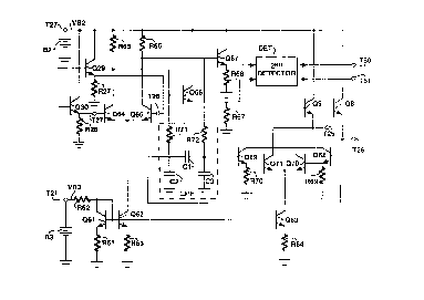
A transistor Q61 is of NPN conductivity type and has
its base and collector electrodes conductively joined so as
to operate in a diode-connected mode. The emitter
electrode of Q61 is connected via a series resistance R61
to a source of a reference potential, here shown as ground.
A reference current is supplied to the joined base and
collector electrodes via a resistance R62 having one end
thereof connected thereto and another end thereof connected
to receive a positive direct bias potential VB3 applied to
the terminal T21. FIGURE 6 shows VB3 as being supplied
from a battery B3. NPN transistors Q62 and Q63 have their
emitter electrodes connected to ground via resistances R63
and R64, respectively, and have their base electrodes
connected to the base electrode of transistor Q61, so as to
form a dual-output current mirror arrangement with respect
to the reference current supplied via R62.
NPN transistors Q64 and Q65 form a differential
amplifier pair, having their respective emitter electrodes
connected to the collector electrode of transistor Q62.
The gain-controlled, amplified, balanced IF signals at the
emitter electrodes of the emitter-follower transistors Q29
and Q30 are applied to the base electrodes of transistors
Q64 and Q65. The collector electrodes of transistors Q64
and Q65 are connected via respective resistances R65 and
R66 to a supply terminal T27 for receiving a positive
operating potential VB2, shown as being supplied from the
~~29854
- 34 -
battery B2. NPN transistors Q66 and Q67 are arranged as
voltage followers of the emitter-follower type, which serve
as output buffer stages. The base electrodes of Q66 and
Q67 connect to the collector electrodes of Q64 and Q65,
respectively, and the collector electrodes of Q66 and Q67
connect to supply terminal T27. The emitter electrodes of
transistors Q66 and Q67 connect to ends of respective load
resistances R67 and R68 the other ends of which connect to
ground.
The emitter electrodes of transistors Q66 and Q67
supply balanced IF output signals superposed on direct bias
potentials to the second detector DET. The second detector
DET supplies an output signal to the terminal T60 and may,
as shown in FIGURE 6, supply another output signal to the
terminal T61, which output signals are balanced in nature.
The second detector DET is the video detector in the case
of a PIX IF amplifier. The second detector DET can be an
intercarrier sound detector in the case where, in addition
to a PIX IF amplifier, another video IF amplifier is used
just for supplying the intercarrier sound detector with
gain-controlled, amplified IF signals generated by
downconverting the RF picture and sound carriers.
The direct bias potentials on which the balanced IF
output signals are superposed are automatically adjusted by
a differential-mode direct-coupled DC feedback loop. The
balanced IF output signals at the collector electrodes of
transistors Q64 and Q65 are supplied to a four-terminal
lowpass filter LPF, which supplies a balanced response to
the base electrodes of common-collector-amplifier NPN
transistors Q68 and Q69. The transistors Q68 and Q69 have
respective emitter load resistors R69 and R70 connecting
from their emitter electrodes to a point at ground
potential.
2~298~~
- 35 -
The balanced response applied to the base electrodes
of transistors Q68 and Q69 essentially consists of the
direct bias potentials on which the balanced IF output
signals are superposed; and transistors Q68 and Q69
function as voltage followers of the emitter-follower type
for applying the difference between these direct potentials
between the base electrodes of NPN transistors Q70 and Q71.
The transistors Q70 and Q71 are connected in emitter-
coupled differential amplifier conjuration. The
interconnection of their emitter electrodes has the
collector electrode of the NPN transistor Q63 connected
thereto, and transistor Q63 withdraws a collector current
from this tail connection that is proportional to the
reference current flowing through the resistance R62, owing
to the current mirror action of transistors Q61 and Q63.
The collector electrodes of the transistors Q70 and Q71 are
connected to withdraw balanced currents from the emitter
electrodes of the previously described emitter-follower
transistors Q9 and Q8, respectively, in response to the
difference between the direct potentials on which the
balanced IF output signals supplied to the second detector
DET are superposed. These connections close the direct
coupled, differential-mode DC feedback loop used for
eliminating any substantial difference between these direct
bias potentials.
The lowpass filter LPF includes a resistance R71 for
connecting the collector electrode Of transistor Q64 to the
base electrode of transistor Q68, a resistance R72 for
connecting the collector electrode of transistor Q65 to the
base electrode of transistor Q69, and a floating
capacitance C1 connected between the base electrodes of
transistors Q68 and Q69. The lowpass filter LPF further
includes two similar capacitances C2 and C3 shunting the
base electrodes of transistors Q68 and Q69, respectively,
2129854
- 36 -
to a point OT points of ground potential. The capacitances
C2 and C3 are relatively small compared to the floating
capacitance C] and supress common-mode signal at the base
electrodes of transistors Q68 and Q69.
The capacitances C1, C2 and C3 are typically of metal-
oxide-semiconductor (MOS) construction. The floating
capacitance C I provides the equivalent filtering action of
two shunt-to-ground capacitances, each twice its
capacitance size. An MOS floating capacitance C1 takes up
l0 only a quarter as much IC die area as two shunt-to-ground
capacitances providing equivalent filtering action. The
floating capacitance C1 may be constructed from two MOS
capacitors of the same size, parallelly connected with the
metal plate of each connecting to the polysilicon plate of
the other. The equal capacitances of the polysilicon
plates to substrate ground appear in respective ones of the
capacitances C2 and C3, then, as at least portions of those
capacitances.
Since the feedback loop used for eliminating any
substantial difference between the direct bias potentials
on which balanced IF signals are superposed is around only
two voltage-gain stages with a maximum voltage gain of a
hundred-fold to two-hundredfold, rather than around three
voltage-gain stages with a maximum voltage gain of a
thousand-fold or more, the primary open-loop pole provided
by the lowpass filter LPF need not be located as low in
frequency in order to assure closed-loop stability. This
reduces the required size of the floating capacitance C1.
The faster time constant in the feedback loop makes it less
prone to "setting up" during impulse noise or start-up
conditions. The use of differential-mode current feedback
to the emitter electrodes of emitter-follower transistors
Q9 and Q8 provides a non-linear feedback response with
mz9~~~
- 37 -
reduced gain for large errors. This also tends to prevent
erratic behavior by the feedback loop during start-up or
impulse noise conditions.
FIGURE 7 shows a modification that can be made to the
FIGURE I gain-controlled amplifier, in which modification
the tee connection of resistors R5, R6 and R7 is replaced
by an equivalent pi connection of resistors R81, R82 and
R83. The resistance of~ R61 equals the sum of the
resistances of R5 and R6;_the resistance of R82 equals the
sum of the resistances of R5 and R7; the resistance of R83
equals the sum of the resistances of R6 and R7.
FIGURE 8 shows a modification that can be made to the
FIGURE I gain-controlled amplifier, in which modification
the tee connection of resistors R44 , R45 and the constant
current source formed by transistor Q42 and resistor R43 is
replaced by an equivalent pi connection of resistor R84 and
two constant current sources, one formed by transistor Q81
and resistor R85, and the other formed by transistor Q82
and resistor R86. That is, the single-output current
mirror comprising elements Q41, R41, Q42 and R43 is
replaced by a dual-output current mirror comprising
elements Q41, R41, Q81, R85, Q82 and R86.
FIGURE 9 shows those portions of a television receiver
or video tape recorder used for recovering audio-signal,
video-signal and synchronizing-signal portions of a
transmitted television signal, which television receiver
uses intermediate-frequency amplifiers Of the type shown in
FIGURE 3 or in FIGURE 5. FIGURE 9 is useful in
understanding how delayed automatic gain control can be
applied to intermediate-frequency amplifiers of the type
shown in FIGURE 3 or in FIGURE 5.
~~~9~5Q-
-' 3 8 -
Television signals captured by an antenna l0 are
supplied to a radio-frequency amplifier 12. A
downconverter 14, which typically includes a mixer and one
or more tunable oscillators oscillating at frequencies
above those in the television signal bands, responds to the
amplified television signals supplied from the radio
frequency amplifier 12 to generate IF signals with sound
carrier at 41.25 MHz and picture carrier at 45.75 MHz. The
downconverter 14 is sometimes referred to as the "first
detector".
The IF signals from this first detector are supplied
to a block filter 16 that separates the sound carrier and
its FM sidebands (and the picture carrier as well in
intercarrier sound receivers) for application to a cascade
connection of a first video IF stage 18, a second video IF
stage 20, and a third video IF stage 22. An on-chip
lowpass filter 24 responds to differences in the direct
bias potentials on which the balanced IF output signals of
the third video IF stage 22 are superposed, to supply
differential-mode feedback signals to summing elements 26
and 28. The summing elements 26 and 28 combine the
differential-mode feedback signals with the balanced output
signals from the first video IF stage 18 to generate
corrected input signals for the second video IF stage 20.
The IF signals from the first detector are also
supplied to a block filter 30 that separates the vestigial
picture carrier and its AM sideband for application to a
cascade connection of a first PIX IF stage 32, a second PIX
IF stage 34, and a third PIX IF stage 36. An on-chip
lowpass filter 38 responds to differences in the direct
bias potentials on which the balanced IF output signals of
the third PIX IF stage 36 are superposed to supply
differential-mode feedback signals to summing elements 40
2i~~~5~-
- 39 -
and 42. The summing elements 40 and 42 combine the
differential-mode feedback signals with the balanced output
signals from the first PIX IF stage 32 to generate
corrected input signals for the second PIX IF stage 34.
A second converter 44, which can be an exalted carrier
synchronous detector in a television receiver generating
sound-IF- signal by the intercarrier method, receives
amplified 45 MHz IF signals from the third video IF stage
22 and responds to generate a frequency-modulated 4.5 MHZ-
IF signal selected by a bandpass filter 46 with a passband
centered at 4.5 MHz. The bandpass filter 46 suppresses the
image frequencies that would otherwise accompany the
frequency-modulated 4.5 MHz sound-IF signal, as applied to
a limiter 48. The limiter 48 suppresses unwanted amplitude
modulation of the frequency-modulated 4.5 MHz carrier it
supplies as sound-IF response to an FM sound discriminator
50, which discriminator detects the frequency-modulation of
the 4.5 MHz carrier to generate the audio signal to be
supplied to the remainder of the television receiver or
video tape recorder. There are other known means for
detecting sound-descriptive information contained in the
frequency modulation of the sound-IF response, which means
include means for suppressing response of said means for
detecting sound-descriptive information to variations in
the amplitude of the sound-IF response, such as the well-
known ratio detector.
A video IF overload detector 52 responds to the
amplified IF signals from the third video IF stage 22
exceeding a level acceptable as input signal to the down
converter 44, to provide an auxiliary automatic-gain-
control (AGC) signal to the first video IF stage 18,
augmenting during abnormal conditions a normal automatic-
gain-control (AGC) signal generated responsive to FIX IF
~.12985~
- 40 -
signal. Under normal conditions, however, both the video
IF and the PIX IF chains are gain controlled responsive
solely to the normal automatic-gain-control (AGC) signal
generated responsive to PIX IF signal. To facilitate the
AGC tracking between the video IF and the PIX IF chains,
the video IF amplifiers 18, 20 and 22 are constructed
within the confines of the same IC as the PIX IF amplifiers
32, 34 and 36. The downconverter 44, the video IF overload
detector 52, a video detector 54, an AGC detector 56 and
AGC delay circuits 58 and 60 are advantageously included
within the same IC as well.
The video detector 54, which receives amplified IF
signals from the third PIX IF stage 36, detects a composite
video signal.
The automatic-gain-control (AGC) detector 56 develops
an automatic-gain-control (AGC) signal by detecting peaks
of the synchronizing pulses included in the composite video
signal. If the video detector 54 is an envelope detector,
the AGC detector 56 is normally a keyed AGC detector in
order to provide the AGC immunity to impulse noise. If the
video detector 54 is a synchronous detector, which is the
modern trend in TV receiver design, the AGC detector 56
preferably includes filtering of its input signal to
suppress response to the 2 MHz or so component of the
composite video signal detected by the video detector 54,
which component arises from the ringing of the block filter
at its midband natural frequency. This filtering of the
input signal of the AGC detector 56 should pass frequencies
up to about 500 kHz; this is so that equalizing pulses can
30 be peak detected and the very top of the video image is not
undesirably increased in brightness respective to the
remainder of the video image. The AGC detector 56 in any
case includes filtering of its output signal to a noise
bandwidth of 400 Hz or so,
21~~8~4
- 41 -
The AGC signal developed by the AGC detector 56
proceeding from the composite video signal detected by the
video detector 38 is used to control gain in both the PIX
IF and the video IF amplifiers as well as gain in the RF
amplifier 12. Developing AGC proceeding from the composite
video signal permits precise gain control of the PIX IF
amplifiers, which have to amplify AM sidebands linearly.
The video IF amplifiers need gain control primarily to
avoid overloading the down-converter 44, gross overloading
of which is forestalled in any case by the video IF
overload detector 52. The linearity with which the FM
sidebands of the sound carrier are amplified is not of
particular concern. The baridpass filter 46 and the limiter
48 suppress the effects of any gain errors in the video IF
amplifier chain and the down-converter 44 as well. So
obtaining acceptable AGC tracking of the video IF
amplifiers 18 and 20 to the PIX IF amplifiers 32 and 34 is
practical to obtain. The AGC signal developed by the AGC
detector 56 is applied in parallel, without delay, to the
second stages 20 and 34 of the video IF and PIX IF
amplifiers. The AGC signal developed by the AGC detector
56 is applied in parallel, with delay, to the first stages
IS and 32 of the video IF and PIX IF amplifiers.
Preferably, as shown in FIGURE 9, the first stages 18 and
32 of the video IF and PIX IF amplifiers have delayed AGC
applied to them via respective AGC delay circuits 58 and
6o, so that only a single AGC line has to be run from the
portion of the IC having the.PIX IF located therein and the
portion of the IC having the video IF located therein.
The AGC signal developed by the AGC detector 56 is
applied to the RF amplifier 12 with still further delay, as
provided by tuner gain control delay circuitry 6o, usually
located on the IF amplifier integrated-circuit chip. Under
=~;eak-signal-reception conditions, any reduction of the gain
212954
- 42 -
through the RF and IF amplifier chains takes place in the
second stages 20 and 34 of the sound and PIX IF amplifiers.
The RF amplifier 12 and the first stages i8 and 32 of the
sound and PIX IF amplifiers, operate at full gain to secure
best signal-to-noise ratios in the signals supplied to the
second stages 20 and 34 of the sound and PIX IF amplifiers.
As second stages 20 and 34 of the sound and PIX IF
amplifiers reach favorable signal levels with increase in
the RF signal level from the antenna 10, the AGC delay
circuits 58 and 60 apply delayed AGC to the first stages 18
and 32 of the sound and PIX IF amplifiers to reduce their
gain. Under strong-signal-reception conditions, the tuner
gain control delay circuitry 62 applies AGC signal to the
RF amplifier 12 to reduce its gain, thereby to avoid
overloading the downconverter 14 and the first stages 18
and 32 of the sound and PIX IF amplifiers.
A dashed line 70 surrounds elements that, except for
large-capacitance shunt bypass capacitors, are normally
constructed within a single monolithic integrated circuit
(IC). The PIX IF chain is operated with balanced signals
throughout, from the input signal applied to the first IF
amplifier stage 32 from the PIX IF block filter 30 to the
output from the third PIX IF amplifier stage 36 to the
video detector 54, and tho output signal from the video
detector 38 is taken single-ended from the IC, to suppress
any self-oscillatory tendencies in the higher-gain portions
of the PIX IF gain control range. The video IF chain is
operated with single-ended input signal applied to the
first IF amplifier stage 18 from the video IF block filter
16, allowing some simplification of that block filter 16,
but the rest of the video IF chain is operated with
balanced signals, to suppress any self-oscillatory
tendencies in the higher-gain portions of the video IF gain
control range. The output signal from the downconverter 44
~i29~5~
- 43 -
is supplied in balanced form to the bandpass filter 46, to
suppress any self-oscillatory tendencies in the higher-gain
portions of the video IF gain control range.
FIGURE 10 shows a suitable block filter 30 response,
presuming a 45.75 MHz video i-f carrier frequency to be
used, which response includes a relatively deep (>40 dB)
trap at the adjacent-channel sound-carrier frequency of
47.25 MHz. This deep trap causes the response to the 45.75
MHz video i-f carrier frequency to be located on a downward
l0 slope in frequency response, about 6 dB down. The response
to the in-channel sound-carrier frequency of 41.25 MHz is
reduced by about 30 dB. The block filter 30 exhibits
linear-phase response throughout its passband. An example
of a SAW filter exhibiting this type of response is the
SAF45 MVB80Z manufactured by Murata Manufacturing Co.,
Ltd., in Erie, Pennsylvania.
FIGURE 11 shows a suitable block filter 16 response
for a TV receiver using intercarrier sound, presuming a
45.75 MHz video i-f carrier frequency to be used, which
response is double-humped in nature. A first of the humps
has a peak at 41.25 MHz, the IF frequency to which the
sound carrier is translated during the first detection
procedure; and a second of the humps has a peak at 45.75
MHz, the IF frequency to which the picture carrier is
translated during the first detection procedure. The block
filter 16 response also includes a relatively deep (>40
dB) trap at the adjacent-channel sound-carrier frequency of
47.25 MHz. The picture carrier is not on a downward slope
into the trap, however, which helps the AFT in
distinguishing the picture carrier from in-channel and
adjacent-channel sound carriers. A saddle between the
humps at 41.25 and 45.75 MHz reduces the =2.25 MHz video
that is detected by the down converter 44, second harmonic
distortion of which video can pass through the 4.5 MHz
2I2985~
- .44
bandpass filter 46 undesirably to affect the limiting of
sound IF by the limiter 48.
FIGURE 12 is a schematic diagram of AGC delay
circuitry suitable for use with the FIGURE 5 cascade
connection of the gain-controlled amplifier stages. An NPN
transistor Q90 has an emitter degeneration resistance R90
and is provided direct-coupled collector-to-base feedback
by an emitter-follower comprising an NPN transistor Q91
having an emitter load resistance R91 connected between its
emitter and a point of reference potential, shown as
ground. The degenerative collector-to-base feedback
adjusts the conduction of_Q90, so as to maintain a voltage
between its emitter and collector that is the sum of the
forward drops across the base-emitter junctions of Q90 and
Q91. The collector current of Q90 flows through the series
connection of resistances R92 and R93 and a diode-connected
NPN transistor Q92 to develop respective voltage drops
across these elements.
The offset from positive operating potential at the
terminal T46 developed by the voltage drop across the
resistance R92 is applied to the base, of an NPN emitter-
follower transistor Q94, the emitter of which provides a
direct bias potential to the terminal T45 and is returned
via an emitter load resistance R94 to a point of reference
potential shown as being ground. The offset from positive
operating potential at the~terminal T46 developed by the
combined voltage drops across the resistances R92 and R93
is applied to the base of an NPN emitter-follower
transistor Q95, the emitter of which provides a direct bias
potential to the base of another NPN emitter-follower
transistor Q96 and is returned via an emitter load
resistance R95 to a point of reference potential shown as
being ground. The emitter of Q96 provides a direct bias
212985
- 45 -
potential to the terminal T23 and is returned via an
emitter load resistance R96 to a point of reference
potential shown as being ground. The combined voltage
drops across resistances R92 and R93 and the diode-
s connected transistor Q92 bias the base of a PNP emitter-
follower transistor Q97. The emitter of Q97 provides a
direct bias potential against which the AGC of the IF
amplifier stages is referred, which direct bias potential
is similar to the direct bias potential applied to the base
of Q95.
A resistive potential divider comprises resistances
R97 and R98 connected between the emitters of Q97 and of an
NPN emitter-follower transistor Q98, which receives AGC
voltage at its base via an AGC terminal T90. The difference
between the AGC voltage as offset by the emitter-to-base
drop of Q98 appearing at the emitter of Q98 and the direct
bias potential appearing at~the emitter of Q97 is divided
for application to the base electrodes of NPN emitter-
follower transistors Q99 and Q100. The emitter of Q99
provides a direct bias potential to the terminal T44 and is
returned via an emitter load resistance R99 to a point of
reference potential shown as being ground. The emitter of
Q99 provides a direct bias potential to the terminal T44
and is returned via an emitter load resistance R99 to a
point of reference potential shown as being ground. The
emitter of Q100 provides a direct bias potential to the
base of another NPN emitter-follower transistor Q101 and is
returned via an emitter load resistance 8100 to a point of
reference potential shown as being ground. The emitter of
Q101 provides a direct bias potential to the terminal T22
and is returned via an emitter load resistance 8101 to a
point of reference potential shown as being ground. (To
provide a more gradual reduction of the voltage gain in the
second controlled-gain voltage amplifier of the IF
~ 1 ~.~854
- 46 -
amplifier before delayed AGC begins to reduce the voltage
gain of its first controlled-gain voltage amplifier, the
transistor Q23 in the second controlled-gain voltage
amplifier has emitter degeneration resistance inserted
between its emitter and the tail connection at the emitter
of the transistor Q24.)
When the AGC potential~applied to the terminal T90 is
insufficiently positive to forward bias the base-emitter
junction of Q98, there is no emitter current flow therefrom
through the potential divider resistances R97 and R98.
Accordingly, the potential drop across each of the
resistances R97 and R98 is essentially zero-valued. The
emitter voltage of Q97 is thus applied to the bases of Q99
and Q100 via R97. The potential at terminal T44 is
consequently less positive than the potential at terminal
T46, biasing the first gain-controlled voltage amplifier
stage of the FIGURE 5 cascade connection for full voltage
gain. Since Q97 is not biased into forward conduction, its
emitter voltage is somewhat more negative than the direct
bias potential applied to the base of Q95. The potential
at terminal T22 is consequently less positive than the
potential at terminal T23, biasing the second gain-
controlled voltage amplifier stage of the FIGURE 5 cascade
connection for full voltage gain.
As the AGC potential applied to the terminal T90
becomes positive enough to forward bias the base-emitter
junction of Q98, the emitter current flow therefrom flows
through the potential divider resistances R97 and R98
causing drops thereacross directly related to the amount by
which the AGC potential applied to the terminal T90 forward
biases the base-emitter junction of Q98. The potential at
terminal T22 approaches the potential at terminal T23,
biasing the second gain-controlled voltage amplifier stage
21~9~~4
- 47 -
of the FIGURE 5 cascade connection for reduced voltage
gain. Owing to the potential drop across R93, the
potential at terminal T44 is still less positive than the
potential at terminal T45, biasing the first gain--
controlled voltage amplifier stage of the FIGURE 5 cascade
connection potential for full voltage gain and delaying the
application of gain control thereto.
As the AGC potential applied to the terminal T90
becomes still more positive, the emitter current flow from
Q98 causes the drop across R97 to approach the drop across
R93. The potential at terminal T44 approaches the
potential at terminal T45, biasing the first gain-
controlled voltage amplifier stage of the FIGURE 5 cascade
connection for reduced voltage gain. As the AGC potential
applied to the terminal T90 becomes still more positive,
the emitter current flow from Q98 causes the drop across
R97 to exceed the drop across R93. The potential at
terminal T44 becomes more positive than the potential at
terminal T45, biasing the first gain-controlled voltage
amplifier stage of the FIGURE 5 cascade connection for
minimal voltage gain.
A terminal T91 can be used for receiving an overload
detector voltage from the video IF overload detector 52 of
FIGURE 9. FIGURE 12 shows the voltage being applied via an
NPN emitter-follower transistor Q102 to one end of a
further potential divider resistance connected 8102 at its
other end to the interconnection of potential divider
resistances R97 and R9F3 causing drops across 8102 and R97
directly related to the amount by which the overload
detector voltage applied to the terminal T91 forward biases
the base-emitter junction of Q102.
The present invention is herein disclosed and its
~m~~~~
- 48 -
principles explained by way of exemplary embodiments, but
is not limited to such embodiments . As will be apparent to
one skilled in the art, various changes and modifications
can be made without departing from the spirit of the
invention. By way of example, with careful layout on the
IC die, the two IF amplifier chains can share some AGC
application circuitry, rather than using separate AGC
application circuitry as described with regard to FIGURES
9 and 12. The invention can be embodied in a television
receiver not utilizing intercarrier sound, with the "video"
IF amplifiers used for amplifying narrower-band IF signals
essentially consisting of the sound carrier wave and its
frequency-modulation sidebands. Television signal
receiving apparatus using plural conversion previous to the
video detector can be constructed in accordance with the
principles of the invention. The controlled-gain
amplifiers herein described utilize NPN amplifying
transistors; clearly, PNP transistors can be substituted
with appropriate circuit modifications as familiar to
persons skilled in the art, or field effect transistors may
be used instead of bipolar transistors, again with
appropriate circuit modifications as are familiar to
persons skilled in the art.
Furthermore, other forms of current mirrors can
replace the particular forms herein used by way of
explanation. It is also contemplated that current steering
need not be achieved by conventional differentially coupled
pairs, though these have the advantage of simplicity, but
it may also be performed by other circuits which can split
an input current into two, components having a variable
ratio. These and like changes are contemplated to be
within the scope of the invention as defined by the claims
following.