Note : Les descriptions sont présentées dans la langue officielle dans laquelle elles ont été soumises.
BC9-93-072 1 21~ 0 4 0 7
STORE IN CACHE HAVING DIRECT SLAVE INTERFACE
BACKGROUND OF THE INVENTION
Field of the Invention
This invention relates generally to personal computers, and
more particularly to personal computers in which performance
is enhanced by a store in cache having a direct slave
interface for eliminating cache data cast out to the main
memory.
Description of Related Art
Modern high speed electronic data processing systems often
comprise a processor or CPU and a hierarchical memory system
including a high capacity relatively low speed main memory
whose cycle time is much less than the cycle time of the
processor and a relatively low capacity high speed memory,
conventionally known as a cache, which has a memory cycle time
comparable to the cycle time of the processor. Such cache
memory systems are well known in the art for reducing
effective memory access time at a more or less reasonable
cost.
The purpose of a cache is to increase the CPU's operating
speed by reducing the number of times that the CPU has to
access main memory for data and instructions. When information
is required by the CPU, it is read from the main memory,
provided to the processor and written into the cache memory.
If the same information is required subsequently by the
processor, it may be read directly from the cache memory to
avoid the time delay which would normally be encountered when
reading the main memory.
There are several cache levels in current hierarchical memory
systems. For example, most high speed microprocessors (e.g.,
Intel 80486), have an internal or private cache (L1) in order
to satisfy the increasing demands of application programs for
more memory and faster operating speeds. In order to further
reduce the access time when the data or instruction is not in
the CPU's private cache, a second level cache (L2) is often
2130~07
BC9-93-072 2
used. The second level cache is external to the CPU, but
supports much faster access times than the main memory.
There are two types of caches that are widely used in current
computer systems. A store through (ST) (or write through)
cache handles read and write operations differently. Data is
written to the ST cache and the main memory regardless of
whether the addressed line is in the cache or not.
Consequently, the cache and the main memory are always in
agreement. This guarantees that the main memory is kept
current and will have the most up to date data. During a read
hit the data is read from the ST cache without accessing the
main memory. However, the disadvantage of a ST cache is that
all writes, which usually average between ten and twenty
percent of all references, are sent to main memory, requiring
substantial main memory bandwidth to avoid significant
performance degradation.
The store in (SI) (or write back) cache has been found to
provide better system performance than a ST cache. In contrast
to the ST cache, the SI cache treats read and write operations
the same. If the line of data specified by an access address
is present in the SI cache, the data will be read from or
written into the cache only. Because all writes are made
directly to the cache without updating main memory, the SI
cache substantially reduces the main memory bandwidth needed
by the CPU compared to a ST cache design.
A problem with a SI cache (Ll and L2) is that the current
information is in the cache and not in the main memory.
Consequently, when any other bus device other than the CPU
attempts to access main memory the SI cache must cast out its
data to the main memory before a read or write operation can
be performed in order to maintain data integrity. For example,
when a main memory read snoop hit OCCUl^S ( cache detects that
a bus master device is trying to read a location in main
memory that only resides in the cache), the cache must first
update the data in the main memory before the bus master
device can read the main memory. The cache will cast out the
line(s) of data corresponding to the address(es) supplied by
the bus master.
21~04Q7
BC9-93-072 3
When a main memory write snoop hit occurs (cache detects that
a bus master device is trying to write to a location in main
memory that already resides in the cache) the cache will also
cast out the addressed line(s) of data to the main memory and
invalidate the corresponding line(s) of data in the cache.
Next, the bus controller will write over the up to date data
in the main memory. The entire line of data in the cache must
be cast out and invalidated even if the bus master is
attempting to write to less than all 16 bytes of the line
because the cache cannot determine which byte(s) of the line
are being accessed.
For example, conventional caches (L1 and L2) can operate in
the following manner. When an input/output (I/O) bus master
initiates a read or a write cycle to a memory location which
is in the cache (L1 or L2), the bus controller (main memory
controller) will drive a control signal CHRDY inactive to
indicate to the I/O bus master that the bus controller is not
yet ready to complete the cycle. Next, the cache will drive a
HITM control signal active which is received by the bus
controller. HITM indicates to the bus controller that the
cache has the up to date data and must transfer it to main
memory before the operation can be performed. The cache will
then cast out the line(s) of data to the main memory (and
invalidate the corresponding line(s) of data in the cache for
write cycles). After the cast out is completed, the bus
controller will drive CHRDY active and then complete the cycle
by sending the line(s) of data to the I/O bus master (read
cycle) or writing new data in the main memory (write cycle).
When a local bus (LB) bus master initiates a read or write
cycle to a memory location which is in the cache (Ll or L2),
the cache will declare a hit while snooping. Next, the cache
will drive HITM active which is input to the main memory
controller to signal that a cast out must occur before the
cycle can be processed. Subsequently, the bus controller will
drive a BACKOFF signal to the LB bus master in order for the
bus master to reinitiate the cycle after the cast out has been
completed. The line(s) of data is then cast out to main memory
and the bus master can then reinitiate the read or write
cycle.
2130407
BC9-93-072 4
Since the cache must cast out its data during a main memory
read snoop hit and a main memory write snoop hit before an I/O
or LB master device can access main memory, system performance
is substantially reduced. In addition, because the
conventional SI caches require an extra step to update the
cache data into the main memory before the bus master can
access the data, Micro Channel~ data streaming can not be
used. Thus, there is a need to develop a store in cache memory
system which eliminates cache data cast out.
SUMMARY OE THE INVENTION
The present invention is directed to direct slave interface
caches which eliminate data cast out to main memory during
read snoop hit and write snoop hit cycles. In one embodiment
of the present invention, the cache is part of a bus interface
controller (BIC) and is coupled directly to a local processor
bus and an input/output bus for receiving address information
from the local and I/O buses and selectively communicating
with one of a local bus (LB~ master and an I/O bus master. The
cache can include one or both of the following: (i) means for
directly transferring data from a memory location in the cache
to the local bus master or the I/O bus master during a read
snoop hit cycle, and/or (ii) means for invalidating data at a
memory location in the cache without casting out the data
during a write snoop hit cycle initiated by the local bus
master or the I/O bus master.
The cache of this embodiment includes a tag array, state array
and memory array each of which is selectively coupled to an
address supplied on the local bus by the local bus master or
an address supplied on the input/output bus by the
input/output bus master. A comparator is used to compare the
address provided to the cache by the selected bus master to
tags in the cache and generate a signal to indicate whether
the address is in the cache. This signal is input to a local
bus cache controller and an I/O cache controller.
When an I/O bus master gains control of the I/O bus and
initiates a read cycle to a byte(s) in a main memory location,
it will place the address of the byte(s) on the I/O bus in
addition to control information indicating what type of
21~0407
BC9-93-072 5
operation (read, write, etc.) is to be performed at that
address. While snooping the cache will detect this cycle. The
I/0 address will be multiplexed into the tag array, state
array and the cache memory array. When the address is present
in the cache a hit will be declared by the comparator. Since
the address is presented directly to the cache memory array,
the data (byte(s)~ will be read out of the cache and provided
directly to the I/0 bus master.
During a write snoop hit cycle initiated by the I/0 bus
master, the I/0 cache controller will generate control signals
which are input to the state array. The control signals are
used to invalidate the valid bits of the byte(s) corresponding
to the selected address location in the cache without casting
out the data to the main memory. Next, the bus interface
controller will write the new data to main memory. The
operation of the cache of the present invention when a local
bus master (other than a CPU) is in control of the local bus
is identical to that described above with regard to an I/0 bus
master.
In another embodiment of the present invention, the cache is
an L1 internal CPU cache or an L2 cache directly coupled to
the local bus. The L1 and L2 caches provide a direct slave
interface during a read snoop hit cycle and/or a write snoop
hit cycle. The L1 and L2 cache can include one or both of the
following: (i) means for directly transferring data from a
memory location in the cache to the local bus master or the
I/0 bus master during a read snoop hit cycle, and/or (ii)
means for invalidating only the byte(s) in the cache that
correspond to the addressed memory location(s) without casting
out the data during a write snoop hit cycle initiated by the
local bus master or the I/0 bus master. During a read snoop
hit cycle, the cache will (i) drive a control signal HITT to
indicate that valid data is in the cache and prevent any other
memory slaves from responding to the bus cycle, and (ii) drive
a READY signal to terminate the read cycle.
The Ll and L2 caches of the present invention include all the
elements of the BIC's cache except for the I/0 interface. More
specifically, the L1 and L2 caches include a tag array, state
21~0~07
BC9-93-072 6
array and memory array each of which being coupled to an
address supplied on the local bus by a local bus master or an
input/output bus master. A comparator is used to compare the
address provided to the cache by one of the bus masters to
tags in the cache and generate an internal signal to indicate
whether the address is in the cache. This signal is input to
a local bus cache controller.
With regard to a bus cycle initiated by an I/0 bus master to
read data from a main memory location having an address, the
I/0 bus master will gain control of the I/0 bus in accordance
with the arbitration procedures of the BIC. The cache will
detect this bus cycle while snooping. The comparator will
compare the memory address with the tags in the tag array and
declare a hit when the address is present in the cache. The
cache controller will then drive the HITT signal in order to
prevent any other memory slaves (Ll cache and BIC memory
controller) from responding. The data will be placed on the
local bus along with the READY signal. Next, the BIC will take
the data and transfer it to the I/0 bus master via the I/0
bus.
If the I/0 bus master is performing a write operation to a
memory location having a corresponding address in the Ll or L2
cache, the local bus cache controller will drive control
signals which will be received by the state array to
invalidate the byte(s) in the L1 or L2 cache corresponding to
the addressed main memory location(s). Next, the BIC will
write the new data to main memory. No cache data cast out
takes place during this cycle. The operation of the Ll or L2
cache of the present invention when a local bus master (other
than the CPU) is in control of the local bus is identical to
that described above with regard to an I/0 bus master.
Thus, if the data in a main memory location addressed by a bus
master (I/0 or local bus master other than the CPU) is also
present in any one of the caches of the present invention a
read snoop hit occurs and the data is transferred (read)
directly from the cache to the bus master without the need for
the cache to first cast out the data to the main memory. If
the bus master issues a write request and the byte(s)
21~0~07
BC9-93-072 7
addressed is in the cache (write snoop hit), the cache will
invalidate the byte(s) for that particular address location
and the bus master can write directly to main memory without
the need for the cache to first cast out the data to the main
memory.
The direct slave interface caches of the present invention
have the significant advantage over prior art SI caches in
that the step to cast out data to main memory during a main
memory read or write snoop hit is eliminated. By eliminating
the extra cast out step, the caches of the present invention
significantly increases the computer's operating speed and is
fast enough to support Micro Channel data streaming.
BRIEF DESCRIPTION OF THE DRAWINGS
Figure 1 is a perspective view of a personal computer
embodying the present invention.
Figure 2 is an exploded perspective view of certain
elements of the personal computer of Fig. 1 including a
chassis, a cover, and a planar board and illustrating certain
relationships among those elements.
Figure 3 is a schematic view of certain components of the
personal computer of Figs. 1 and 2.
Figure 4 is a general block diagram of one embodiment of
the direct slave interface cache of the present invention.
Figure 5 illustrates the control and directory
organization of the direct slave interface cache of Fig. 4.
Figure 6 is a block diagram representation of the
elements and connections of the direct slave interface cache
of Fig. 4.
Figure 7 is a general block diagram of another embodiment
of the direct slave interface cache of the present invention.
Figure 8 is a general block diagram of a further
embodiment of the direct slave interface cache of the present
invention.
Figure 9 is a block diagram representation of the
elements and connections of the direct slave interface caches
of Figs. 7 and 8.
2130~7
BC9-93-072 8
DETAILED DESCRIPTION OF THE INVENTION
While the present invention will be described more fully
hereinafter with reference to the accompanying drawings, in
which a preferred embodiment of the present invention is
shown, it is to be understood at the outset of the description
which follows that persons of skill in the appropriate arts
may modify the invention here descrlbed while still achieving
the favourable results of this invention. Accordingly, the
description which follows is to be understood as being a
broad, teaching disclosure directed to persons of skill in the
appropriate arts, and not as limiting upon the present
invention.
Referring now more particularly to the accompanying drawings,
a microcomputer embodying the present invention is there shown
and generally indicated at 10 (Fig. 1). The computer 10 may
have an associated monitor 11, keyboard 12 and printer or
plotter 14. The computer 10 has a cover 15 which cooperates
with a chassis 19 in defining an enclosed, shielded volume for
receiving electrically powered data processing and storage
components for processing and storing digital data, as shown
in Fig. 2. At least certain of these components are mounted on
a multilayer planar 20 or motherboard which is mounted on the
chassis 19 and provides a means for electrically
interconnecting the components of the computer 10 including
those identified above and such other associated elements as
floppy disk drives, various forms of direct access storage
devices, accessory cards or boards, and the like.
The chassis 19 has a base and a rear panel (Fig. 2) and
defines at least one open bay for receiving a data storage
device such as a disk drive for magnetic or optical disks, a
tape backup drive, or the like. In the illustrated form, an
upper bay 22 is adapted to receive peripheral drives of a
first size (such as those known as 3.5 inch drives). A floppy
disk drive, a removable media direct access storage device
capable of receiving a diskette inserted thereinto and using
the diskette to receive, store and deliver data as is
generally known, may be provided in the upper bay 22.
2130~Q7
BC9-93-072 9
Prior to relating the above structure to the present
invention, a summary of the operation in general of the
personal computer system 10 may merit review. Referring to
Fig. 3, there is shown a block diagram of a personal computer
system illustrating the various components of the computer
system such as the system 10 in accordance with the present
invention, including components mounted on the planar 20 and
the connection of the planar to the I/O slots and other
hardware of the personal computer system. Connected to the
planar is the system processor 32 which can optionally have a
direct slave interface internal L1 cache 33 according to the
present invention. The CPU 32 is connected by a high speed CPU
local bus 34 to a bus interface control unit 35, to volatile
random access memory (RAM) 36 (main memory) here shown as
Single Inline Memory Modules (SIMMS) and to BIOS ROM 38 in
which is stored instructions for basic input/output operations
to the CPU 32. The BIOS ROM 38 includes the BIOS that is used
to interface between the I/O devices and the operating system
of the microprocessor 32. Instructions stored in ROM 38 can be
copied into RAM 36 to decrease the execution time of BIOS.
While the present invention is described hereinafter with
particular reference to the system block diagram of Fig. 3 it
is to be understood at the outset of the description which
follows that it is contemplated that the apparatus and methods
in accordance with the present invention may be used with
other hardware configurations of the planar board. For
example, the system processor could be an Intel 80486
microprocessor.
Returning now to Fig. 3, the CPU local bus 34 (comprising
data, address and control components) also provides for the
connection of the microprocessor 32 with a direct slave
interface L2 cache 37 in accordance with the present
invention. In addition, a numeric or math coprocessor (MCPU)
39 and a Small Computer Systems Interface (SCSI) controller 40
are connected to the CPU 32 hy the local bus 34. The SCSI
controller 40 may, as is known to persons skilled in the arts
of computer design and operation, be connected or connectable
with Read Only Memory (ROM) 41, RAM 42, and suitable external
devices of a variety of types as facilitated by the I/O
- 21304Q~
BC9-93-072 10
connection indicated to the right in the Figure. The SCSI
controller 40 functions as a storage controller in controlling
storage memory devices such as fixed or removable media
electromagnetic storage devices (also known as hard and floppy
disk drives), electro-optical, tape and other storage devices.
The bus interface controller (BIC) 35 includes a store-in
direct slave interface cache 43 according to the present
invention. The BIC 35 couples the CPU local bus 34 with an I/O
bus 44 and functions as a protocol translator, memory
controller and DMA controller among other functions. By means
of the bus 44, the BIC 35 is coupled with an optional feature
bus such as a Micro Channel bus having a plurality of I/O
slots for receiving Micro Channel adapter cards 45 which may
be further connected to an I/O device or memory (not shown).
The I/O bus 44 includes address, data, and control components.
The I/O bus 44 may be configured to bus specifications other
than the Micro Channel specification.
Coupled along the I/O bus 44 are a variety of I/O components
such as a video signal processor (VSP) 46 which is associated
with video RAM (VRAM) for storing character based information
(indicated at 48) and for storing graphic or image based
information (indicated at 49). Video signals exchanged with
the processor 46 may be passed through a Digital to Analog
Converter (DAC) 50 to a monitor or other display device.
Provision is also made for connecting the VSP 46 directly with
what is here referred to as a natural image input/output,
which may take the form of a video recorder/player, camera,
etc. The I/O bus 44 is also coupled with a Digital Signal
Processor (DSP) 51 which has associated instruction RAM 52 and
data RAM 54 available to store software instructions for the
processing of signals by the DSP 51 and data involved in such
processing. The DSP 51 provides for processing of audio inputs
and outputs by the provision of an audio controller 55, and
for handling of other signals by provision of an analog
interface controller 56. Lastly, the I/O bus 44 is coupled
with an input/output controller 58 having associated
Electrical Erasable Programmable Read Only Memory (EEPROM) 59
by which inputs and outputs are exchanged with conventional
peripherals including floppy disk drives, a printer or plotter
21~04~7
BC9-93-072 11
14, keyboard 12, a mouse or pointing device (not shown), and
by means of a serial port.
Before turning in greater detail to a description of the
present invention, it is appropriate to first consider the
support by a personal computer of what has been known as
multiple bus masters or bus masters. As here used, a "master"
is a processor or any circuit designed to gain control over a
bus and drive address, data and control signals on the bus.
Having such capability enables a master device to transfer
information between system memory and other devices.
It has been proposed that masters be divided among three types
-- system master (usually the CPU), DMA controller, and bus
master. The system master controls and manages the system
configuration. It is usually the default master in the system.
The default master owns the bus when no other master requires
it. A DMA master is a special type of master which transfers
data between DMA slaves and memory slaves, and does not
arbitrate for the bus but services the DMA slave that is the
arbitrator. As here used, a bus master arbitrates for use of
the bus and supports information transfers with an I/0 slave
or memory slave.
What makes a device a "bus master" can be confusing, as bus
masters do not necessarily require a processor. Also, a bus
master may be called on to respond as a slave when accessed by
another bus master. A bus master is distinguished by the
capability of gaining control of the bus through arbitration
and controlling the execution of a defined bus cycle.
Generally, there are three types of bus masters: full
function, special function controllers, and programmable
special function controllers. The fundamental differences
among them are degrees of flexibility, function and cost. The
full function bus master is the most flexible, has the most
function, and costs most. Typically, a full function bus
master will have its own programmable CPU and be capable of
controlling all system resources, including operating system
software. Special function controllers have the least
flexibility, function and cost. Typical1y, a special function
controller will use logic circuits but no CPU to perform a
213040~
BC9-93-072 12
specific function while requiring little or no assistance from
other masters. Programmable special function controllers span
the range between the other two. The fundamental difference
between special function and programmable special function
controllers is the ability to modify the function and/or
execution characteristics of the bus master. Such modification
can be accomplished through use of processing units or through
settable registers.
Within the definitions here given, the CPU 32, MCPU 39, and
SCSI controller 40 may all function as masters directly
coupled to or on the local bus 34, while the I/O controller
58, DSP 51, VSP 46 and possibly accessory boards 45 mounted in
the Micro Channel slots may all function as masters directly
coupled to or on the input/output bus 44.
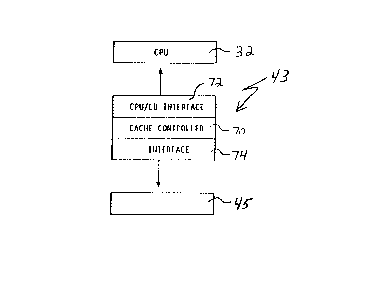
Referring to Fig. 4, there is shown a general block diagram of
one embodiment of the direct slave interface cache 43 of the
present invention. The cache 43 is incorporated within the BIC
35 and includes a cache controller 70, a local bus (LB)
interface 72 and an input/output (I/0) interface 74. The cache
43 is coupled to the CPU 32 by the LB interface 72. In
addition, the cache 43 is coupled directly to I/0 devices by
the I/0 interface 74. Thus, the cache 43 has two interfaces
for bidirectionally transferring data directly to a local bus
master or an I/0 bus master via the LB and I/0 buses
respectively. It should be understood that the present
invention is not limited to an interface 74 to the I/0 bus 44
but can be an interface to any type of secondary bus coupled
to the I/0 bus 44 such as, for example, the Micro Channel bus
using Micro Channel adapter cards 45, Peripheral Component
Interconnect (PCI) bus (not shown) or Video Electronics
Standards Association (VESA) bus (not shown).
A general overview of the operation and advantages of the
cache 43 will be described in connection with Fig. 3. The
cache 43 is a store-in cache which conventionally includes a
snooping capability. The cache 43 constantly checks requests
made by devices other than the CPU 32 that wish to access main
memory 36 to see if the requested address is in the cache 43.
When an I/0 device such as, for example, DSP 51 gains access
- 21304~7
BC9-93-072 13
to the I/0 bus 44 and drives a cycle to read a byte(s) in main
memory 36, the cache 43 will detect such a read request while
snooping and check to see if the data is duplicated in the
cache 43. If the byte(s) addressed by the DSP 51 is in the
cache 43, a read snoop hit occurs and only the byte(s)
addressed are transferred (read) directly from the cache 43 to
the DSP 51 without the need to access the main memory 36.
If the DSP 51 issues a write request and the byte(s) addressed
is in the cache 43 (write snoop hit), the cache 43 will
invalidate only the byte(s) corresponding to the address
supplied by DSP 51. Next, the BIC 35 can write directly to
memory 36 without the need for the cache 43 to first cast out
the data to the main memory 36. When a request is made by the
DSP 51 for an address that is not in the cache 43, the cache
43 is inactive and the read or write snoop miss cycle is
conventionally performed in the main memory 36.
Turning now to Fig. 5, there is shown the control and
directory organization of the dual bus interface cache 43 of
the present invention. The cache 43 is a four way set
associative cache. Cache data is stored in a static random
access memory (SRAM) array 84 comprised of four banks (A, B,
C, D) each of which being 32 bits (one word) wide and 32 bits
deep for a total of 512 bytes. Although the present invention
is not limited to such a sized cache array, the remaining
explanation will be based upon these numbers for illustrative
purposes.
The most significant 19 address bits corresponding to each
entry in the four banks of data is saved in four 19 bit groups
for a 32 x 19 TAG array 80 for each bank. Each byte for each
address location in each bank has a corresponding valid bit
such that if a particular byte is present in the SRAM array 84
then the valid bit for that byte is on, and if a particular
byte is not present in the SRAM array 84, then the valid bit
for that byte is off. Since there are four bytes in each
address location there are four valid bits associated with
each address for a total of 16 valid bits. Three least
recently used (LRU) bits are used to indicate which of the
four banks of data will be replaced by a new entry when the
2130407
BC9-93-072 14
cache is full in accordance with a conventional LRU algorithm.
The three LRU bits and the 16 valid bits comprise a 19 x 19
state or LRU/VALID array 82.
Referring to Fig. 6, there is shown a schematic diagram of the
cache 43 of the present invention. The TAG array 80, state
array 82 and SRAM array 84 each have four inputs and one
output. The four inputs include an Address, Data In, Clock and
Bit Write Control input. A LB cache controller 86 receives a
plurality of inputs including HLDA, ADS#, M/I0#, W/R#, and
HIT/MISS (internal). HLDA is a control signal used to
distinguish a local bus cycle initiated by the CPU 32 from a
local bus cycle initiated by a local bus master (other than
the CPU 32). ADS#, M/I0# and W/R# are control signals which
are driven by the local bus master in control of the local bus
34 when HLDA is high. The ADS# line is the local bus address
status indicator, and it is driven by the local bus master to
indicate that a valid local bus cycle is available. If there
is a valid local bus cycle (ADS# low) then M/I0# indicates
whether the valid LB cycle is either a memory (M/I0# high) or
an I/0 (M/I0# low) cycle. W/R# is a local bus master driven
cycle definition signal used to indicate a Write (W/R# low) or
a Read (W/R# high) cycle.
A comparator 90 is used to compare the address provided to the
cache 43 by the I/0 or LB bus master to the tags in the TAG
array 80. Accordingly, if the address is present a hit is
declared by comparator 90 by driving HIT/MISS active--low.
When the address is not present in the TAG array 80, the
comparator 90 declares a miss by driving HIT/MISS high. The
TAG array 80, LRU/VALID array 82 and the SRAM array 84 receive
the LB or I/0 address via multiplexers 92, 94 and 96
respectively depending on whether the local bus master or the
I/0 bus master is driving the bus cycle.
An I/0 cache controller 88 also receives the output of
comparator 90 (HIT/MISS) to determine if a requested address
location resides in the cache 43. The I/0 cache controller 88
also receives inputs S0#, Sl#, ADL#, I/O_M/I0# and CMD#. Each
of these control signals is driven by an I/0 bus master in
control of the I/0 bus 44. S0#, S1#, and I/O_M/I0# are
2130~07
BC9-93-072 15
decoded by the I/0 cache controller 88 to determine whether
the I/0 bus cycle is either a memory read (S0# high, Sl# high,
I/O_M/I0# high), memory write (S0# high, S1# low, I/O_M/I0#
high), I/0 read (S0# high, Sl# high, I/O_M/I0# low), I/0 write
(S0# high, S1# low, I/O_M/I0# low), or an interrupt
acknowledge bus cycle (S0# low). The signal CMD# is active low
and is used to define when data is valid. ADL# is used to
indicate a valid address and its status.
The LB and I/0 cache controllers 86, 88 each generate two
output signals. The LB_LRU/VALID and I/O_LRU/VALID outputs are
used to indicate which bytes of a selected word are valid and
the bytes that will be replaced by the LRU algorithm when
necessary. These outputs along with LB_BIT_WR_CNTL and
I/O_BIT_WR_CNTL are inactive during a read hit and are used to
invalidate the byte(s) of an address location during a write
snoop hit from a LB or I/0 bus master respectively.
In order to provide a complete understanding of the direct
slave interface cache of the present invention a description
of the operation thereof will be described hereinafter. As an
illustrative example and referring to Figs. 3 and 6, the MCPU
39 and SCSI 40 are local bus masters coupled directly to the
local bus 34 while the I/0 controller 58, DSP 51, VSP 46 and
possibly accessory boards 45 mounted in the MC slots may all
function as I/0 bus masters coupled directly to or on the I/0
bus 44. While any appropriate microprocessor 32 can be used in
this embodiment, one suitable microprocessor is the 80386
which is sold by INTEL.
In operation, the direct slave interface cache 43 will be
snooping on the I/0 bus 44 as is conventionally done in a
store-in-cache. (The details of such a snooping implementation
is system dependent, not a part of the present invention and
many variations are possible.) The cache 43 will watch the I/0
bus 44 to make sure that any requests to access a location in
main memory 36 is not present in the cache 43. For example,
after an I/0 bus master device such as I/0 controller 58 gains
control over the I/0 bus 44 through arbitration, it can drive
a read cycle. The I/0 bus master 58 will place the address of
the byte(s) at the memory location that it wishes to access on
2130407
BC9-93-072 16
the I/O bus 44. The S0#, S1#, and I/O_M/IO# signals will be
driven by the I/O bus master 58 to the appropriate levels to
indicate that a valid I/O bus cycle is beginning and what type
of operation is to be performed.
The I/O address will be multiplexed into the TAG array 80,
LRU/VALID array 82 and SRAM array 84. This address will be
compared to tags in TAG array 80 and a hit will be declared by
comparator 90 if the address is present in cache 43. When
there is a hit, the HIT/MISS signal will be asserted active
and input to the I/O cache controller 88. Since this is a read
cycle, the I/O_LRU/VALID output is not used and the
I/O_BIT_WR_CNTR will be set to inactive. Since the address was
presented to the SRAM array 84 by multiplexer 96 the byte(s)
of data will be read out of the SRAM array 84 and multiplexed
onto the I/O bus 44 by multiplexer 98. Thus, during a read
snoop hit cycle initiated by the I/O bus master 58, the
requested byte(s) are transferred directly from the cache 43
to the I/O bus master 58 without cache data cast out.
When the bus cycle initiated by the I/O bus master 58 is a
write cycle, the I/O cache controller 88 will set the
I/O_BIT_WR_CNTL signal LOW--active and will set the valid bits
for the addressed byte(s) on I/O_LRU/VALID to invalid. The LRU
bits are not affected as these bits are set from the LB side
by the LB masters. These signals will then be received by the
LRU/VALID array 82 and the valid bits for the byte(s)
corresponding to the address supplied by the I/O bus master
will be changed to invalid to invalidate the selected byte(s)
in the cache 43. Next, the BIC 35 will write the new data to
main memory 36. Thus, during a write snoop hit, the cache
byte(s) are invalidated without cache data cast out. This is
a significant improvement over conventional caches which must
invalidate and cast out an entire line of data during a write
snoop hit even when less than all of the bytes in the line of
data are being addressed by the I/O bus master 58.
Similarly, when a LB bus master other than CPU 32 such as, for
example, MCPU 39 wishes to perform a read operation it will
place the address of the memory location it wishes to read on
the local bus 34 after it gains control of local bus 34
21~0407
BC9-93-072 17
through arbitration. The ADS# and M/IO# signals will be driven
by the MCPU 39 to the appropriate levels to indicate that a
valid local bus cycle is beginning and what type of operation
is to be performed. The LB address will be multiplexed into
the TAG array 80, LRU/VALID array 82 and the cache RAMS 84 by
multiplexers 92, 94 and 96 respectively. When the address is
present in the TAG array 80, the comparator 90 will drive
HIT/MISS active. This signal will then be input to the LB
cache controller 86. The LB_LRU/VALID output does nothing and
the LB_BIT_WR_CNTR will be set to inactive. Since the address
is presented to the cache RAMS 84 the data (byte(s)) will
simply be transferred directly from the cache RAMS 84 to the
local bus 34 by multiplexer 98.
When a write cycle is initiated by the LB bus master 39 the LB
cache controller 88 will set the LB_BIT_WR_CNTL signal LOW--
active and will set the valid bits corresponding to the
addressed byte(s) on LB_LRU/VALID to invalid. (The LRU bits
will be set by the LB master according to a conventional LRU
algorithm.) These signals will then be received by the
LRU/VALID array 82 and the valid bits for the address selected
will be changed to invalid to invalidate the selected byte(s)
in the cache 43. Next, the BIC 35 will write the new data to
the corresponding byte(s) in main memory 36 without waiting
for the cache 43 to first cast out the data.
If the I/O bus master 58 or the LB bus master 39 requests a
read or a write operation to be performed at a memory location
that is not in the cache 43 (read or write snoop miss),
HIT/MISS will be driven inactive high by comparator 90. The
cache 43 will not respond to the cycle and the read or write
operation is then conventionally performed directly in main
memory 36.
Referring now to Fig. 7 and 8, there are shown block diagrams
of alternative embodiments of the present invention wherein
the CPU's internal cache 33 (Fig, 7) or the external L2 cache
37 (Fig. 8) can be a direct slave interface cache. The caches
33 and 37 have the following modifications as compared to
conventional L1 and L2 caches in order to provide a direct
slave interface during a read snoop hit cycle: 1) drive an
21~0 10~
BC9-93-072 18
output control signal HITT (active low) to indicate that valid
data is in the cache and prevent any other memory slaves from
responding to the bus cycle, and 2) drive the bidirectional
READY signal (active low) to terminate the read cycle. In
contrast to a conventional L1 or L2 cache (READY is received
as input only), the L1 and L2 caches 33 and 37 of the present
invention will have a bidirectional READY signal so that it
may drive this signal and act as a memory slave. In addition,
in contrast to conventional L1 and L2 caches, the caches 33
and 37 also provide a direct slave interface during a write
snoop hit cycle by invalidating only the byte(s) in the cache
that correspond to the addressed memory location(s) without
casting out the data to main memory.
Since the direct slave interface L1 and L2 caches 33, 37 of
the present invention are identical in operation, the
description below will be directed to the L2 cache 37 but it
should be understood that it is equally applicable to the L1
cache 33. Of course it should be understood by those skilled
in the art of the present invention that the L1 cache is
typically much smaller than the L2 cache. In addition, the L1
cache of the present invention can be implemented in any
microprocessor having an internal cache that requires data
cast out when a read snoop hit or a write snoop hit occurs in
the internal cache such as, for example, INTEL's P5 and P24T
Pentium microprocessors.
Turning now to Fig. 9, the L2 cache 37 includes all the
elements of the cache 43 shown in Fig. 6 except for the I/0
interface and all like elements have been labelled with the
same reference numerals. More specifically, cache 37 does not
include an I/0 cache controller nor any signals relating
thereto. In addition, multiplexers 92, 94 and 96 have been
removed since the cache 37 is only coupled to an address
supplied on the local bus 34. The control and directory
organization of the L2 cache 37 can be identical to that
described above with regard to cache 43.
Referring to Figs. 3 and 9, when a LB bus master other than
CPU 32, such as, for example, SCSI 40 initiates a read cycle
to a particular memory location in the main memory 36, it will
2130407
BC9-93-072 19
place the address of that location on local bus 34. The ADS#,
M/I0# and W/R# signals will be driven by the SCSI 40 to the
appropriate levels when HLDA is high as described above. The
cache 37 will detect the read cycle while snooping. The LB
address will be sent into the TAG array 80, LRU/VALID array 82
and the cache RAMS 84 over local bus 34. HIT/MISS will be
asserted by comparator 90 when the address is present in the
cache 37 and the valid bit for the byte(s) at this address is
set. This signal will then be input to the LB cache controller
86.
Next, the LB cache controller 86 will drive the HITT signal
active--low on the control portion of local bus 34. This
signal will be received by other memory slaves such as the Ll
cache 33 and the BIC memory controller (not shown) to indicate
to these devices that they should not respond to the cycle
since the data is in the L2 cache 37. Since it is a read cycle
the LB_LRU/VALID output does nothing and the LB_BIT_WR_CNTR
will be set to inactive. Since the address is presented to the
cache RAMS 84 the data (byte(s)) will simply be transferred
out of the cache RAMS 84 and placed on the local bus 34.
Simultaneously with the data transfer, the cache controller 86
will drive the READY signal on the control portion of local
bus 34 to indicate the end of the cycle. Thus, the cache 37
operates as a memory slave to the local bus master 40.
When the operation to be performed is a write operation, the
LB cache controller 86 will set the LB_BIT_WR_CNTL signal low
and will set the valid bits on LB_LRU/VALID to invalid. These
signals will then be received by the LRU/VALID array 82 and
the valid bits for the byte(s) selected will be changed to
invalid to invalidate the byte(s) in the cache 37
corresponding to the addressed main memory location. The BIC
35 can then write the new data to main memory 36. No cache
data cast out takes place during this cycle. The cache 37 does
not cast out its data because each byte(s) invalidated in the
cache 37 corresponds to each byte(s) addressed by the LB bus
master 40. This is a significant improvement over conventional
caches which must invalidate and cast out an entire line of
data during a write snoop hit even when less than all of the
- 2130407
BC9-93-072 20
bytes in the line of data are being addressed by the LB bus
master.
With regard to a cycle initiated by an I/0 bus master such as,
for example, DSP 51, it will gain control over the I/0 bus 44
in accordance with the arbitration procedures of the BIC 35.
The I/0 bus master 51 will then drive control signals ADS#,
M/I0# and W/R# to the appropriate levels when HLDA is high as
discussed above to initiate a bus cycle to read a byte(s) of
data from a memory location in main memory 36. The L2 cache 37
will detect this request while snooping. When the byte(s) of
data is also present in the SRAM array 84 and a corresponding
valid bit is set the following events will take place. The
comparator 90 will compare the memory address on local bus 34
with tags in TAG array 80 and drive the HIT/MISS signal active
to indicate a valid cache access. The controller 86 will then
drive the HITT signal in order to prevent any other memory
slaves (L1 cache 33 and BIC 35 memory controller) from
responding. The data byte(s) will be placed on local bus 34
along with the READY signal and transferred to the I/0 bus 44
by the BIC 35 and then to the I/0 bus master 51.
When the I/0 bus master 51 initiates a write cycle to a memory
location which is in the L2 cache 37 with valid data, the LB
cache controller 86 will set the LB_BIT_WR_CNTL signal Low--
active and will set the valid bits on LB_LRU/VALID to invalid.
These signals will then be received by the LRU/VALID array 82
and the valid bits for the byte(s) addressed will be changed
to invalid to invalidate the selected address location in the
cache 37. Next, the BIC 35 will write the new data to main
memory 36 without the added delay associated with cache data
cast out. No cache data cast out takes place during this cycle
because each byte(s) invalidated in the cache 37 corresponds
to each byte(s) addressed by the I/0 bus master 51.
If the LB bus master 40 or the I/0 bus master 51 requests a
read or a write operation to be performed at a memory location
that is not in the L2 cache 37, HIT/MISS will be driven
inactive high by comparator 90. The cache 37 will not respond
to the cycle and the read or write operation is then
conventionally performed directly in main memory 36.
- 21~0407
BC9-93-072 21
By eliminating the extra cast out step, the direct slave
interface caches 33, 37 and 43 of the present invention can
support a Micro Channel data streaming protocol when the I/0
bus 44 is coupled to the optional Micro Channel bus. The Micro
Channel requires that an address be defined before allowing a
word to be transferred over its bus. Two cycles are thus
required for each transfer of one word--one for setting up the
address and one for moving the data. Usually, an entire block
of data is moved at a time, one word after another. In such
situations, the address for each byte becomes redundant after
the first transfer is completed. The Micro Channel data
streaming protocol cuts the time to transfer a word in half by
eliminating every other cycle (the addressing cycle) of a
transfer of a block of sequential data words. Consequently,
for transfers of blocks of data, streaming data mode
effectively doubles the transfer rate.
In summary, the direct slave interface caches 33, 37 and 43 of
the present invention have the significant advantage over
prior art SI caches in that the step to cast out data to main
memory during a main memory read snoop hit or a main memory
write snoop hit is eliminated. By eliminating the extra cast
out step, the direct slave interface caches significantly
increase the operation speed of a personal computer system
utilizing such caches and is fast enough to support Micro
Channel data streaming protocol.
In the drawings and specifications there has been set forth a
preferred embodiment of the invention and, although specific
terms are used, the description thus given used terminology in
a generic and descriptive sense only and not for purposes of
limitation.