Note : Les descriptions sont présentées dans la langue officielle dans laquelle elles ont été soumises.
` 2131799
WQ9411~15 -1 PCT1~31~107
A FL~XIBLE D~VICE FOR ENcApBuLaTING ELECTRO~S~ CoMpoN~NTs
TECHNICAL FIELD
The present invention relates to a device for encapsulating
electronic components orcircuitry such as to protect the electric
circuit against substances which may act deleter~ously thereon,
wherein the device alsoattenuates radiofrequency electromagnetic
radiation so as to protect the circuit against such radiation that
can enter from the surroundings and disturb the function of the
circuit through induction, said devic~ also being active to
protect the surroundings when the circuit concerned constitutes
a disturbance or interference source. The device includes
throughlet conductors which allow circuit-functional current and
signals to be applied when required.
TECHNICAL FIE~D
It is often necessary to protect electronic circuits against
different infl~ences emanating from the surroundinqs. Factors
which influence electronic circuitry include water and other
corrosive and electrically conductive materia. It is also often
important to protect the circuitry against electromagnetic
radiation. In this regard, there is traditionally used different
types of capsules which can be roughly divided into two main
groups, hermetic capsules and plastic capsules. In the case of
hermetic capsules, the electronic circuitry is surrounded by a
clean and dry volume of gas enclosed in a diffusion-impervious
casing, normally a metal, glass or ceramic casing. When the casing
is made of metal, glass throughlets are fused in the metal casing
for leading electrical conductors between the encapsulated
circuitry and the ambient surroundings. When a plastic capsule is
used, the circuitry is surrounded by plastic material instead of
clean or pure gas. Although the plastic material is permeable to
water and gases, it will nevertheless often pr~vide satisfactory
protection, because coherent films are unable to form on the
surfaces of the circuit components. Furthermore, plastic material
has a more or less pronounced ability to bind chemically with the
2 2131799
wos4/~ PCT1~ 3/~10~
,- .
polar groups present in the surface of the circuit ComponentS~
These groups are thus blocked so as to be unable to form corrosion
attack sites. The differences in the coefficient of thermal
expansion between the different materials present constituteS a
problem in both types of capsule. Another problem is that the
circuitry is often so sensitive as to react against compound5
which are split or cleaved from the actual encapsulating mate-
rials. A third problem is that polymeric material is often unable
to withstand the working temperatures concerned, particularly as
rises in temperature are often local, spotwise temperature in-
creases, wherewith the plastic encapsulating materials connect
directly on to these points. This can result in degradation of
properties and spalling of the corrosive substances. In the case
of plastic capsules, it is often difficult to conduct heat away
from the electronic circuitry to the surroundings and they have no
electrically shielding ability. In addition to these technical
problems, there is often a low price interest.
The levels of these various requirements vary, although they are
particularly stringent in thecaseof electronic circuitry foruse
in cars and radio communication systems for instance. Several
attempts have been made to glue hermetic metal and ceramic
capsules, although it has been found difficult to obtain glue
joints which are age-resistant and impervious. For the purpose of
packaging electronic circuitry which is sensitîve to electric
discharge caused by static electricity, encapsulating bags have
been developed which include a casing comprised of plastic sheets
on which thin metal layers have been applied by vapour deposition.
These principles cannot be applied, however, in advanced encap-
sulation, since the metal layers obtained by vapour deposition or
sputtering do not have a thicknesswhich renders the enc~psulation
impervious to diffusion. Furthermore, with regard to radio
frequency radiation, the depth of current penetration is many
times greater than the depth of penetration in the case of a metal
layer and consequently the resistivity in the casing is too high
to attenuate such radiation effectively and therewith provide an
efficient shielding effect.
3 2~31799
W094/1~15 PCT
DISCLOSURE OF THE INVENTION
The object of the present invention is to avoid those problems
which exist with present-day electronic circuitry encapsui~ting
devices. In accordance with the invention, there is provided to
this end a device in which the electronic circuit~y is encased,
either completely or partially, in a casing which is comprised of
a plastic and metal-sheet laminate. The metal sheet, or sheets,
has/have a thickness at which it/they is~are diffusion-impervious
and electrically shielding, with regard to the necessary electri-
cal conductivity and at the then prevailing penetration depths ofthe electric currents atthe frequency concerned, or corresponding
~ise times in the case of digital transmission. The device may
include a laminate which comprises several metal sheets and
intermediate plastic sheets, therewith providing extremely
effective diffusion-impervious and shielding properties, while
obtaining a casing which is highly flexible and pliable, and
enabling the casing to be readily given a bag-like configuration.
The casing is closed and sealed with the aid of an adhesive, by
thermal welding techniques, or by means of mechanical clamps.
Electrical conductors are laminated in one section of the casing
sealing location in a manner to obtain an impervious join between
the electric conductors and the laminate. The bag is thus imper-
viously sealed by means of joints and electric signals and
electric current can be passed tothe electronic circuitry through
the electrical conductors. The casing joints and the joints
between the casing and the electric conductors are constructed so
that the diffusion path between the plastic-metal laminate is so
long, compared with the area in the plastic material which is
perpendicular to the diffusion direction, as to enable the amount
of contaminants, for instance water, that can diffuse into the bag
during the lifetime of the electronic circuitry to be ignored in
relation to the volume of gas enclosed.
One advantage afforded by the invention is that the device
provides a practically diffusion-impervious and electrically~
shielded, inexpensive encapsulation. Manufacturing costs arevery
low. Those parts of the electronic circuitry which develop heat
.
WO94/1~15 4 213 I 7 9 9 pcl~sEg3loo~o7
can be cooled by bringing these parts into abutment with a large
surface area on the inner surface of the casing and by applying
cooling means to a corresponding surface area on the outer surface
of the casing, so as to carry away or transfer the heat generated.
The metal sheets in the casing can be connected directly to the
electrical earth surfaces of the circuitry, so as to conduct away
the induced currents in an electrically shielding function. The
composition of the gas enclosed together with the circuitry can be
checked in conjunction wit~ sealing the casing, and the gas volume
can be analyzed at any desired time, for instance with the aid of
a masspectro~eter, with the intention of checking the concen-
tration of contaminants in the casing, for instance water. A gas
sample can be taken through a very small opening in the casing,
which is then preferably resealed, for instance in the same way as
the remaining casing joints were achieved. When required, other
devices may be incorporated in the casing for carrying light or
heat, for instance.
BRIEF DESCRIPTION OF THE DRA~ING
Figure 1 is a sectional view of a flexible device for encap-
sulating electronic circuitry in accordance with the present
invention.
Figure 2 is an enlarged, sectional view of one corner of the
inventive encapsulating bag.
B~ST MODE OF CARRYING OUT THE INVENTION
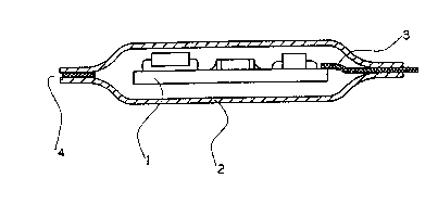
Figure 1 illustrates a typical device for flexibly encapsulating
electronic circuitry. The device includes an electronic circuit
board 1 which is fully enclosed by a bag 2. The bag 2 is sealed,
for instance, by fusion-welded joints in the joint region 4.
Electrical c~nnections are achieved with the aid of electrical
conductors 3 sealingly embraced in a part of the joint region 4.
Figure 2 illustrates part of the device in larger scale. The bag
is comprised of a laminate structure 2 consisting of metal sheets
6 laminated between plastic sheets 5 in a manner such that the
~Og4/1~15 5 21 31 79 9 PCT1~ 31~107
.
plastic sheets S adhere sealingly to the whole of the surfaces of
the metal sheets 6. The laminate structure 2 from which the bag is
made is closed sealingly in the joint regions 4. ~he metal sheets
6 form a diffusion barrier against low molecular substances that
are liable to damage the electronic circuit board. It is highly
improbable that any damaged areas and pores 7, 8 in the metal
sheets 6 will lie close together in the laminate structure 2. When
seen in relation to the area extendinq perpendicularly to the
diffusion direction, the diffusion paths of the penetrating
contaminants in the laminate structure 2 and the joint region 4
are very long, and also in those points in the laminate structure
2 where defects in the form of pores 7, 8 in the metal sheets 6 are
located. As will be understood, the length of the diffusion paths
in relation to the area at right angles to the diffusion direction
and also the thickness of the laminate structure 2 have been
greatly exagqerated in the Figure, for the sake of illustration.
In the illustrated embodiment, the laminate 2 is comprised of the
following sheets, as seen from the outer surface of the casing:
PolyethyleneterephthalateO.023 ~m,aluminium 0.014 mm, polyethy-
lene terephthalate 0.023 ~m and, furthest in, low-pressure
polyethylene 0~075 ~m. The casing joints are formed by fusing the
low-pressure polyethylene sheets together at a temperature of
150-C and a pressure of lO0 N/cm .
According to another embodiment, certain parts of the casing are
advantageously joined to metal parts, for instance to carry away
heat, or to a glass window through which a display on the electro-
nic board can be seen. According to a further variant of the
inventive device, a joint is advantageously formed between the
electronic circuit card and the casing. In those instances where
joints are desired with other materials than the actual laminate
2, for instance with metal, glass or with circuit board surfaces,
that side of the laminate 2 which is to be heat-welded to these
materials is comprised of polyethylene which has been modified
with carboxyl groups which have been c~oss-linked with zinc ions,
so-called ionomer plastic. Such plastics have the ability to form
bonds with many different types of surfaces, so as to obtain a
joint of satisfactory mechanical strength. In these cases, the
~ WO ~/1~1~ 6 2 1 3 1 7 9 9 PCT~3/~107
, . .
fusion welding process can be effect:ed at 130-C and at 100 N/cm2
It will be understood that other variants are conceivable, t~ese
further variants being limited sollely by the scope of the fo:-
lowing Claims.