Note : Les descriptions sont présentées dans la langue officielle dans laquelle elles ont été soumises.
213~ 3
~'0 93/237~9 PCTt~'S9~/03
Apparatus and method for the l~nearizat~on of the s~gnal transfer of an
integrated optical phase modulator comprising modulators coupled in cascade.
Related Application
The presen~ invention is related to Applicant's co-
pending application Serial No 07/706,911, filed May 29, 1991, and
- entitled "APPARATUS AND METHOD FOR LINE~RIZED CASCADE COUPLED
INTEGRATED OPTICAL MO~ULATOR", which 'is incorporated herein by
~ reference.
¦ Field Of The Invention
This invention relates generally to modulators, and
I more particularly to a method and apparatus for providing
j linearized signal transfer in integrated electro-optical phase
¦ 5 modulators.
!
¦ ,Back~round Of The Invention
Integrated electro-optical modulators are finding
-' increasing use in state-of-the-art analog optical-fiber
communication systems. Such systems are being developed as an
1~ alternati~e to conventional electromagnetic transmission lines.
, Present optical-fiber communication systems may consist of a high
power, low noise laser source in conjunction with a wide
bandwidth external modulator, for example. Such external
modulators may be used in conjunction with high power, low noise
2~fi~. 2~
Wog3~237xs PCT/~'S93/03~
las2rs, to provide analog signal transfer in optical fiber cable
T.V. networks. A common problem in such systems is that the
dynamic range thereof is limited by intermodulation distortion,
and by harmonic distortion due to modulator nonlinearities. Many
attempts have been made in the art to improve the linearity of
the modulators.
One method of improving the linearity of optical
modulators is to provide electromagnetic predistortion of the
input signal. A system for accomplishing this is reported in an
article by R.P. Child~ and D.A. O'Byrne, that appeared in OFC 90,
entitled 7'Predistortion Linearization of Directly Modulated DFB
Lasers and External Modulators for AM Video Transmission."
There are many examples of electro-optical modulators,
demodulators, and modulating systems in the art. A number of
such prior systems are briefly discussed below.
- Johnson U.S. Patents 5,015,053 and 5,002,355 refer to
linearization of an interferometric modulator by coupling to
transverse electric (TE) and transverse magnetic (TM) modes. A
carrier wave derived from a light source is polarized by a
polarizer for adjusting the power of the carrier wave in the TE
and TM polarization modes.
Hamilton et al. U.S. Patent 5,010,346 shows an electro-
optical analog-to-digital converter. A laser light source is
synchronized with a digital clock for producing pulses of light.
The pulses of light are modulated by an optical modulator for
varying the intensity of the pulses of light as a function of the
amplitude of the analog modulating signal. The light pulses are
W0~3/~3789 ~ ~ ? ~ PCT/~'S93/O~X(~(
demultiplexed and passed through a detector for converting the
light pulses to electrical signals. The electrical signals are
- then passed through an electrical analog-to-digital converter.
DuPuy et al U.S. Patent 4,997,245 shows optical
switches that are polarization independent. The optical switches
include a substrate of electro-optic material in which waveguides
are formed in a manner permitting light waves to be switched
therethrough independent of polarization phenomena.
Thylen U.S. Patent 4,993,798 refers to an optical
communication system consisting of a semiconductor laser that
includes an optical waveguide coupled at one end to first and
second optical directional switches. The other ends of each one
of the directional couplers each have an end of a waveguide
terminated to a mirror, for forming a cavity including the laser
diode. By either modulating current driving the diode, or by
i applying a modulating signal to the directional couplers, a light
signal passing therethrough can be modulated.
Yoon et al U.S. Patent 4,936,645 shows a polarization-
insensitive Mach-Zehnder modulator that includes a thin film
waveguide on a substrate. The modulator consists of a lamination
of different organic polymers upon which the thin film waveguide
is deposited, and electrodes for applying voltages for producing
electric fields to coact with the light passing through the
waveguides.
Xoai U.S. Patent 4,934,776 teaches the combination of
cascaded individual waveguide directional coupler sections
arranged to provide a high-density optical data array, for
2 ~ ~ 6 1~ 2 i~ :~
W093/23789 PCT/~'S93~03~f~
forming an integrated optical intensity modu?~tor. The cascaded
~ !",
coupled-waveguide modulators provi~e~ult~a-high extinction
ratios. ~ ~:
Koai U.S. Patent 4,9~q;775 ~shows an optical space-
division switching architecture consisting of high-extinction
electro-optical data arrays of a plurality of cascaded coupled-
waveguide optical intensity modulators. A plurality of passive
splitter circuits are used to evenly divide an input optical
signal into a plurality of interim optical signals. The optical
signals are passed through the optical intensity modulators,
respectively, which have waveguide coupler sections cascaded
together on a crystal substrate to form a bar-type modulator
; structure, for providing a direct optical connection between the
various sections of each modulator. Combiner circuits receive
the output optical signals from the data arrays and com~ine them
for providing a single output wave or signal.
Su U.S. Patent 4,932,736 teaches thè monolithic
integration of three integrated waveguide couplers to provide a
lX2 or 2Xl integrated optical switch with a high extinction
ratio. In the switch a first waveguide coupler has its output
directly coupled to the input ports of the other two waveguide
couplers via an integrated waveguide. As a result, two cascaded
integrated waveguide couplers are provided along each path from
a single input port to two output ports, respectively.
Coleman U.S. Patent 4,882,775 shows a demodulator
provided by a an interferometer and a signal processor. The
demodulator is included in a coherence multiplexed, optical data
, W093/23789 ~ 2 1 3 6 2 2 9 PCT/~'S9~/03~
transmission system. The optical data transmission system
includes an in~erferometric modulator at an input end. The
output signals therefrom are modulated waveforms which are passed
through an optical multiplexer, and coupled via single mode
S optical couplers and a fiber optic cable to demodulator stages.
Each modulator and demodulator stage is provided by an unequal
-arm-length Mach-Zehnder interferometer. The multiplexers phase
modulate the optical carriers from the modulators for
¦multiplexing the same toge~her. The path lengths between the
modulators and demodulators included in the system are controlled
for obtaining a desired output from the output demodulator stages
40.
iAlferness U.S. Patent 4,390,236 shows an electro-
cptical demultiplexer consisting of a plurality of cascaded
tunable, polarization independent optical wavelength filters.
The various sections of the filters, as cascaded, provide an
-input polarization selective coupler that separates the
transverse electrical (TE) and transverse magnetic (TM)
orthogonally polarized wave components, respectively, of an
20 arbitrarily polarized input signal. The separated TE and TM
components then travel along two different wavepaths or
waveguides. Each waveguide includes a wavelength selective mode
converter. An output polarization selective coupler is provided
for combining in one output waveguide signal components centered
about the wavelength of the mode con~erters, and for combining
in a second output waveguide the balance of the input signal~
2136229
WO93/2378s ` PCTt~'S9~/03X~)~
Papuchon U.S. Patent 4,223,977 shows an integrated
optical circuit for separating a pluræ,,lity of optical waves of
, ti ~`
different wavelengths, thereby ~pr~viding a demultiplexing
function. A plurality of basic electro-optical cells are
integrated on a single substrate for providing the optical
demultiplexing circuit.
I A paper entitled "Waveguide Modulators with Extended
Linear Dynamic Range a Theoretical Prediction" (Z.Q. Lin and
W.S.C. Chang, Photonics Technology Letters, Vol. 2, No. 12, Dec.
'90) shows a modifièd-directional-coupler modulator with reduced
nonlinear distortion. The coupler includes an input stage for
receiving input signals for a voltage control directional coupler
that couples the signals to a Mach-Zehnder interferometer. The
output of the interferometer is coupled by a fixed directional
coupler to an output waveguide providing two channels. The
parameters are adjusted for minimizing third order
intermodulation spurious signals.
A paper entitled "In Search of a Linear Electro-optic
Amplitude Modulator" (Pao-Lo Liu, B.J. Li, and Y.S. Trisno, SPIE
Conference, 1990) shows a linear electro-optic amplitude
modulator. The modulator includes a Y-branch for dividing an
optical input signal equally for inputting into the two arms,
respectively, of a Mach-Zehnder interferometer. The
interferometer functions as a phase shifter. The output of the
interferometer is supplied to a directional coupler having a
nominal coupling constant-length product of half a coupling
length. The optical output signal is provided at each of two
SUBSTITIJTE SHEET
2 P 7 4 3 9
~136229
output waveguides. A modulation signal of one polarity is
applied to the interferometer phase shifter, and is applied in
reverse polarity to the directional coupler using a
multiplication factor. The parameters are adjusted for
optimizing the linearity of the modulator by reducing the second
and third order harmonics that cause nonlinearities to occur.
The present inventor recognized that known integrated
optics modulators require further improvement. One need
recognized is to improve the linearity of integrated optical
phase modulators.
In a paper entitled "Linearization Of Electro-Optic
Modulators By A Cascade Coupling Of Phase Modulating Electrodes"
(Halvor Skeie and Richard ~. Johnson, SPIE Conference, Vol. 1583, -
Integrated Optical Circuits, Sept. 1991, p. 153) shows two -
configurations for linearized optical modulators for use in wide
Figure 4 shows an optical phase modulator :~
band analog transmission systems. T~e~ c~ri~}e~b~scadi~g
formed by a cascaded Y-branch input, a first phase modulator, a first coupler, -`
~ a6*~-Ze~ Q~ t~ t~Ee~ ow~ a second phase modulator, a second ::~
coupler and output waveguides. The figure also depicts bias electrodes for the ~`
phase modulators. :~
SUMMARY OF THE INVENTION
An object of the present invention is to provide an
improved integrated optical phase modulator with complementary
output signals.
Another object of the invention is to provide an
integrated optical phase modulator having increased linearity and `~
complementary output signals.
These and other objects of the invention to overcome
the problems in the prior art and satisfy the identified need are
AMEND~D SHE{~
Z -~ P 7439
-` 2136229
~-.
i provided in one embodiment of the invention by an integrated
optical phase modulator including a Y-branch power splitter for
receiving a light input signal, splitting the same into two
output signal~, and passing the output signals to a first phase
modulator controlled by a signal voltage V~(t). A pair of output
signals from the first p~ase modulator are corrected as input -.
signals via a first fixed, co~pler with coupling angle ~ to a -.
second phase modulator controlled by a signal voltage V2~t). A
pair of output signals from the second phase modulator are
connected as input signals to second fixed coupler with coupling
angle ~, the latter providing complementary output signals of the
cascaded modulator. In another embodiment, a 3 dB coupler is `
substituted for the Y-branch power splitter. .
".
Brief Desçri~t on of the Drawin~s
Various embodiments of the present invention are
illustrated below in conjunction with the accompanying drawings,
wherein like items are identified by the same reference
designation, and in which:
Figure l is a simplified pictorial diagram showing a
linearized single coupler with one rf input ~e~-~n~ ~i~n~
e--~e~iOA;
Figure 2 is a plot or curve of the transfer function
for optimized linear operation of the single coupler of Figure
l; .
E~
r~2 P 7439 2 1 3 6 ~ 2 9 `
Figure 3 is a simplified pictorial diagram of a phase
modulator A~ coupl0r cascade switch
i~;
Figur~ 4 is a curve showing the coupling angle ~ as a
5function of rf weighting for the phase modulator of Figure 3;
Figure 5 is a curve showing the relative sensitivity
as a function of rf weighting for the phase modulator of Figure
3;
Figure 6 is a curve showing a transfer function for the
10phase modulator-coupler cascade of Figure 3, for ~ = 45, and
k = -0.95;
Figure 7 is a curve showing the third harmonic
suppression (dB) as a function of modulation index m (dB) for the
phase modulator-coupler cascade of Figure 3;
15Figure 8 shows a simplified pictorial diagram of
cascaded rf phase modulators of one embodiment of the invention;
Figure 9 is a curve showing the relative coupling angle
(~/90) as a function of rf weighting for the cascaded modulators
of Figure 8;
20Figure lO is a curve showing the relative rf
sensitivity as a function of rf weighting for the cascaded
modulators of Figure 8;
Figure 11 is a curve showing a transfer function of the
cascaded phase modulators of Figure 8 for ~ = 27 and
25 k = -0.5;
AMENDE~ SHEF~
21~6229 ~ ~ :
WO 93/237~9 - ` i i ? ., PCT/~'S93~03X(~(
Figure 12 is a curve showing the third harmonic
suppression as a function of modulating index m for the cascaded
modulators of ~igure 8;
Figure 13 shows a simplified pictorial diagram of
s cascaded rf phase modulators for another embodiment of the
invention;
Figure 14 shows a simplified pictorial diagram of
cascaded rf phase modulators for a preferred embodiment of the
invention; and
Figure 15 shows a simplified schematic and pictorial
diagram of an engineering prototype for the embodiment of Figure
14.
Detailed Descri~tion Of Preferred Embodiments Of The Invention
The linearized optical phase modulator embodiments of
the present invention, as described below, may be considered
linearized optical guided waveguide (OGW) modulators. In the
various embodiments of the invention, each provides two
complementary light output signals which offers advantages over
prior modulators having only a single output signal. In the
present embodiments of the invention, the complementary output
signals are substantially of the same power level and are equally
linear, thereby splitting the available laser power. Another
advantage is that one of the complementary.output signals may be
used as a control signal, preferably in a closed loop system, for
providing a bias adjustment to optimize and stabilize the
linearity of the cascaded modulators.
10
SUBSTlllJTE SHEET
2136229 ~:
In Figure 1, an improved linearized single coupler 1,
having a single rf terminal 3 for receiving an rf input signal
rf(x) is shown. Assuming an ideal coupler structure, coupler 1
includes two cascaded sections S and 7 having coupler lengths e1
! 5 and e2, respectively. An upper horizontal waveguide segment 9
conducts a light input signal ajn to a downward sloping waveguide
segmént 11 for providing an input laser light signal to the
coupler 1. Also shown, but typically not used for providing a
light signal to the coupler 1, is a lower horizontal waveguide
segment 13, for conducting a light signal bjn into an upward
sloping waveguide segment 15 for delivering the light signal bj"
to coupler 1. The first coupler section 5 includes in the
integrated structure shown a portion of a horizontal waveguide
segment 17 for receiving light input signal ajn from waveguide
segment 11, a portion of a lower waveguide segment 19 connected
at one end to an output end of waveguide se~ment 15, an electrode
j 21 overlying an associated portion of waveguide 17, and an
electrode 23 overlying an associated portion of waveguide i9.
The terminal 3 is connected to electrode 21 for providing the rf
signal rf(x) thereto, where x is an angular value representing
the rf signal amplitude relative to the switching voltage.
Electrode 23 is connected to a source of reference potential,
ground in this example. Note that waveguides 17 and 19 are
substantially parallel to one another as are electrodes 21 and
23.
The second coupler section 7 includes the remaining
portions of waveguide segments 17 and 19, in this example. An
electrode 25 overlies an associated portion of waveguide 17. An
AMENDED S`r~EET
2136229
W093/23789 PCT/~'S93/03X()(
electrode 27 overlies an associated portion of waveguide 19.
These elements are substantially parallel to one another. A bias
terminal 29 is provided for connec~ing a DC bias voltage V~ to
electrode 25. Electrode 27 is ~nnected to ground, in this
example. A lisht output signal from the cascaded first and
second coupler sections 5 and 7 is conducted from waveguide
segment 17 through an upwardly sloping waveguide segment 31, and
through a horizontal waveguide segment 33 to provide an a~, light
output signal. Similarly, a light output signal b~, is conducted
from the other end of waveguide segment 19 through a downwardly
; sloping waveguide segment 35, and following horizontal waveguide
I segment 37 to provide a b~, light output signal that is
- complementary to the a~, light output signal. As previously
- mentioned, these complementary light output signals a~, and b~,
are substantially equally linear, and of the same power level.
Note that the various waveguide segments are typically formed on
a lithium niobate crystal substrate (not shown), with the
i waveguide segments 9, 11, 13, 15, 17, 19, 31, 33, 35, and 37
being formed by diffusing titanium into the substrate. The
electrodes 21, 23, 25, and 27 are typically deposited on top of
the substrate, and typically may consist of metals such as a
first adhesion layer of chrome (typically 100 Angstroms thick),
followed by a thick layer of aluminum (up to 10,000 Angstroms).
Note also that the shape of any of the electrodes and waveguides
illustrated in the various embodiments herein are not meant to
. , , . . ~ .
WO 93~3789 Q 1 3 6 2 2 g PCr/l 'S93/03~6
be limiting in that many shapes or configurations can be used
therefor.
¦ Assume that the coupler structure of Figure 1 is an
¦ ideal one and that t~e two cascaded sections 5 and 7 have ¦~
coupling angles ~ and ~dr respectively, with no external voltages
applied. Let the rf coupling be ~ x . The two input-two
output coupler 5,7 is described by its 2 x 2 transformation
¦ matrix M, as follows in equation (1):
( hout) = M ( b'n) (1)
where "a", "b" represent complex signal amplitudes of the
parallel waveguides.
The rf section 5 transmission matrix is described as
follows:
I cos~+jyx sin~ jysin~ (2)
j~f l-jysin~/~, cos~ - jyxsin~
where
j = ~1, ~ = Y~
x is proportional to the input signal voltage rf(x).
The dc bi~s section 7 is described as follows:
.
M ¦ Cos<l)d~jydqsinl~l)d/~pd ~ --jy~)dSiIld~d/~
jydsin~3d/~pd, COS!pd jydxsin~l)d/~pd ¦
2136229 -
W093/237X9 PCT/~'S93/03X~
~t~
where ~d is r~__ t.
q being proportional to the applied dc voltage.
To simplify calculations, equation 3 is rewritten as follows: :
¦ cosae~ j sina¦ (4)
dC _j sina, cosae~J~
where
tan(~) = q ~ tan(~d)
q2
~ 5 and
f sin (~d)
q2 .~
The cascade coupling 5,7 is described as follows:
Mc = Md~ Mrf
with signal input a~, b~ = 0, the signal transfer for output a~,
is described by ~ as follows:
Mt11 = cosaJ~ ~ (cos~ , j (yx sin~ (sina y sin~ 6)
= re ~ j im
2136229 ~
` W093/23789 PCT/~IS9~/03Xl)( ~
where re, im represent the real and imaginary parts, ~::
respectively. :
~ ~ .
The output power proportional to the detected signal is as
follows:
P/Pin = Ie2 ~ im2 = f (x) t7)
The series expansion for f(x3 is as follows: ;
f(x) f(o) ~ df/dxto) x+l/2 d2f/dx2 (o) x2~1/6 d3f/dx3 ( ) 3 `~
~8) ::
In order to suppress second and third order distortion, the
following relations are required~
d2f/dx2(o) = o, d3f/dx3() = ( )
From equation (7) one can derive the following: :
df/dx = 2re re' + 2im im'
d2f/dx2 = 2re'7 + 2re re" -2im'2 + 2im im" tlO)
d3f/dx3 = 6re' re" ~ 2re re"' ~ 6im' im"+ 2im im"'
where ~, n ~ and ~' denote first, second, third derivatives.
From equations (6) and (2), one can derive the following:
re'(0) = 0
re"(0) = -~sin~ cos~-sin~ cos~ (~ cos~-sin~)
re~'(0) = 0 tll)
im'(0) = sin~-sin~-sin~ :
im"(0) = sin~ sin~(~ cos~-sin~
imU~(O) = 3 cos~(~ cos~-sin~)
From equation (9) and (10), one obtains the following:
d2f/dx2(0) = (0) (12)
:
2136229 ~
W093/237~9 PCT/~'S9~/03
From equation (12) it can be shown that:
sin2(~) sin(~) cos(~) - 0 ;`'. ~13)
In addition if: r;`
.~ `''s.
d3f/dx3(0~ = (0)
then (14)
~ - tan~ = 0
Solving for ~ from equation (14~, one obtains:
~ = 2.86 ~/2 - 257.4
The modulator sensitivity is proportional to the following:
10df/dx(0) - sin~(~) sin2(~) sin(~) ~15
! A practical solu~ion to equation (13)-is therefore as follows:
, cos~ = 0, ~ = ~/2, 3~/2 etc. ~16)
i ~or maximum sensitivity: :
sin (2~) = 1 or ~ = ~/4 ~17)
! 15 From equation (3), one can obtain the following values:
~d = 7~/2
~d = ~ 63.6 q = 1.0 (18)
A plot of a transfer function for optimized linear
operatisn of the ~ coupler of Figure 1 is shown in Figure 2,
with ~ = 257.4, ~d = 63.6, and q = 1Ø
A phase modulator 41 in series with a ~ coupler 43,
as shown in Figure 3, provides a phase modulator A~ cascade
switch 45. An input light wave P~, typically having a power
level expressed in milliwatts, is applied to an input waveguide
47, for carrying the light wave Pu) to be divided into upper
1~
- -, , -, - - - . ... .
` W093/237~ 2 1 3 6 2 2 9 PCT/~Sg~/o~
waveguide segment 49 and lower waveguide segment 8 of the Y-
waveguide 47, 49, 51. Light from the upper segment 49 travels
through a longitudinal upper waveguide segment 53, through an
upper downward sloping waveguide segment 55, through an upper
longitudinal and horizontal waveguide segment 61, through an
upwardly sloping waveguide segment 69, and therefrom through a
longitudinal end horizontal waveguide segment 73 for providing
an output signal P~,. Similarly, lower waveguide segment 51
receives substantially half of the light signal P~ and condu~ts
the same to travel through lower longitudinal and horizontal
waveguide segment 57, therefrom through upward sloping waveguide
~egment 59, through lower horizontal waveguide segment 63,
through downward sloping waveguide segment 71, and therefrom
through lower horizontal waveguide segment 75, for providing from
the latter a light output signal P~,. P~l is complementary to the
upper output signal P~t, in this example. A horizontal electrode
77 is both parallel and overlying to upper waveguide segment 53,
for receiving via conduc~or 81 an rf input signal rfl. A lower
electrode 79 is provided in parallel with and overlying the lower
waveguide segment 57, as simplistically shown for purposes of
illustration. Lower electrode 79 is connected to ground, in this
example. The combination of waveguide segments 53 and S7, and
electrodes 77 and 79, provide a phase modulator.
An electrode 65 is provided in parallel and overlying
2~ upper waveguide segment 61, and another electrode 67 is provided
in parallel with and overlying lower waveguide segment 63. An
electrode terminal 83 is provided for conducting to electrode 61
17
,, .,. "".. ,,,,,~,,., . . , , ~ ,
2136229
W093/23789 PCT/~'S93/03~
a second rf modulating signal rf2. Electrode 67 is connected to
ground, in this example. The combination of waveguide segments
61 and 63, and electrodes 65 and 67 form a -A~ coupler. Note
that the length of the phase modulato~ section 41 is shown as a
~, whereas the -~ coupler 43 has a length e2
Assuming an ideal, balanced configuration, rf
electrodes 77, 79 with length eJ will generate a phase shift 2x
between the two arms or waveguide segments 53 and 57 of phase
modulator 41. The coupling angle of the ~ coupler 43 is:
= 2x' (19)
where x' = kx.
The ratio k = x'/x is proportional to the ratio of the
two rf input signals rf, and rf2 provided the electrode geometrics
of electrodes 65 and 67, and associated impedance matching
circuitry ~not shown) are similar.
1~ The phase modulator 41 transmission matrix is:
¦ ejx 0 ¦ (20
The -~ coupler section 43 matrix is as follows:
I cos~+jx'sin~ jysin~ t21)
c I -jysin~/~, cos~-jXsin~
~- .
2 P 74~9 2136229
where
/y 2 ~ -X 1 2
The total matrix is then as follows:
j eiX~cos~+~x~sin~ je~iXy~in~ (22)
t -jejxy sin~/~, e~~X(cos-jx~sin~
The output power is:
f(x) = (P~, + P~,)/P~ = l/2 Imt,l ~ mtl2l2 (23
From equation (22):
-mt~l + mt~2 = cosx cos~ - sin~ sin~ x'sinx sin~/~
+ (5 inx cos~x'cosx sin~ cosx (sin~ ) (24)
By substitution into equation (23):
f(x) = 0.5 - sin~/~-(sin(2x) cos~x' cos(2x) sin~/~) (25)
By successive derivation of f(x) with respect to x, one
obtains:
sensitivity dfldx(0) = - sin(2~)-0.5 k(1-cos(2~ 26)
Second order distortion is expressed as follows:
d2f/dx2(0)=0 for all values of k,~ (no bias) ~27)
Third order distortion is as follows:
d3fldx3(0) = 0 for k3+a2k2+alk+aO = 0 ~28)
19
AMENDED S~lET
~2 P 74~9 2136229
where
aO - - 4sin(2~ ~3/3 (~sin(2~) + cos(2~
a~ ~ - 2(1~cos(2~ 2 (~sint~) + cos(2~ 29)
a2 = - (2~cos(2~-sin(2~ sin(2y~ + cos(2~
s From (28) and (26) the coupling angle ~ and the
sensitivity df/dx (0) for third.order distortion compensation can
be found as function of the rf weighting k.
Results from these calculations are shown in Figures
4 and 5, for curves showing coupling angle ~ as a function of rf
weighting, and relative sensitivity df/dx as a function of rf
weighting, respectively.
It appears from Figure 5, that a reasonable sensitivity
is obtained for weighting factors in the range of -0.5 to 1.5.
Corresponding ranges for coupling angles are 45 to 65 and 105~
to 140. Consider as an example, ~ = 45. The calculated
transfer function is shown in Figure 6 as a plot of relative
input intensity as a function of relative input signal. Figure
7 shows relative harmonic distortion as a function of modulation
index m.
In Figure 8, an~4~ embodiment of the invention is
shown for cascading two phase modulators 85 and 87 with two fixed
couplers 89 and 91. In comparison with the modulator em~od~en~
of Figure 3, each receives two input signals rfl and rf2, for
example, but a ~ coupler region such as 43 is avoided in the
embodiment of Figure 8.
~M~NDED SHEFr
~ `` W093/237X9 2 1 3 6 2 2 ~ PCT/~'S93/03~
Phase modulators 8s and 87 have similar structure as
~hase modulator 41. One difference is that phase modulator 87
I is configured for receiving via input electrode 81 the rf input
! signal rf2, and waveguide segments 49 and S1 receive
complementary light signals from a coupler 89.
Also, in modulators 85 and 87, relative to modulator
41, electrodes 77 and 79 are located between, proximate, and
parall~l to waveguide segments 53 and 57, respectively, and
electrically connected together by bridging electrode 82.
Electrodes 88 and 86 are located proximate and in parallel with
the other sides of wavegulde segments 53 and 57, as shown in this
- example. Electrodes ~8 and 8Ç are connected to a source of
reference potential, ground in this example.
I The fixed coupler 89 has a length Qc~ and includes two
parallel waveguide segments 93,95, for coupling output waveguide
segment 55 to input waveguide segment 49, and output waveguide
59 to input waveguide segment 51, of phase modulators 85 and 87,
respectively. ~ixed coupler 91 is substantially similar to
coupler 89, and consists of parallel waveguide segments 97 and
99 for ~oupling output waveguide segments 55 and 59,
respectively, from phase modulator 87, to upward and downwardly
sloping waveguide segments lOl and 103, respectively, in this
example. Waveguide segments lOl and 103 have their other ends
connected to an end of upper and lower horizontal and parallel
waveguide segments 105 and 107, respectively. The other ends of
the waveguidP segments 105 and lQ7 provide complementary
modulated light output signals P~ and P~l, respectively. Note
21
W093~23789 2i362æg ~ PCI/l'S93/03t~(16
that phase modulators 85 and 87 have l'e~ths of ~, and e2 ,
respectively, which are typically substantially equal.
In the embodiment of Figure 8, the total transmission
matrix consists of four cascaded section matrices as given below
in equations (30), (31) and (32). Assume the fixed couplers 89
and 91 have identical coupling, their transmission matrix Mc is
as follows in equation (30):
M I cosy,-jsiny
j - jsiny, cosy
Rf phase modulator 85 has a transmission matrix Mpl as
follows: :
Mpl = ¦ O e~~ 31)
Note that 2x, obtained in solving the matrix Mpl, is the phase
difference in the two arms.
Similarly, for the second phase modulator 87, its
transmission matrix is M~ as follows in equation (32):
I e~'~O ¦ (32)
where x' = kx , and k = rf weighting factor.
... . . . . . . . . . . . . . ... . .. .. .. . . . . . . ..
I W093~237X9 2 1 3 6 2 2 9 ` PCT/~'S93/03~t\(.
¦ The total matrix is the sum of the individual matrices
as shown below in equation (33): ~-
~ = MCMnM~pl ~33) ~.
Accordingly, ~ can be expressed as shown below in equation (34): .
¦ cos2ye~ sin2ye~2,-jsinycosy~e~j~+e~i~2) ¦
S c I ~j sinycosy(e'~l~ej~2), cos2~le~i~l-sin~ye~j~2
,, ,~;:
where ~ = x~x' and ~2 = X-X~.
The relative output power is as follows in eguation
(35): '
F(x) = P/P~ = 1/2 (re2+im2) ~35) ~
where :
lo re = cos2~ cos~l - sin2~ cos~2 -sin~ cos~ (sin~, + sin~2),
and
im = cos2~ cos~, - sin2~ sin ~2 -sin~- cos~ (cos~ + cos~2).
'
From successive derivation:
Sensitivity df/dx(0) = -sin(2~)(2cos(2~)+k) ~36)
.
Second order distortion is expressed by:
d2f/dx2~0) = 0 for all values of k,~(no bias) ~37)
Third order distortion is expressed by:
d3f/dx3(0) = 0 for k3+3cos(2~)k2+3k+2cost2~) = 0
2 P 7439 2136229 ` :
From equations (36) and (38) the coupling angle ~ and
the sensitivity df/dx(O) for third order compensation can be
determined as a function of rf weighting. Results are shown in
Figures 9 and 10, for plots showing (~/90) as a function of rf
s weighting, and rf sensitivity as a function of rf weighting,
respecti~ely~
Figure 10 shows that an optimum operating point in
terms of rf sensitivity is obtained if k ~ -0.5. This
corresponds to a coupling range ~ of 0.3(90~) = 27. The
calculated transfer function for this case is shown in Figure 11,
for relative input intensity as a function of relative input
signal. The corresponding suppression of third harmonic
generation as function of modulation index m is shown in Figure
12.
In evaluating switch modulators with regard to
practical implementation, from the standpoint of simplicity in
~odulator
both design and rf feeding circuitry, the embodim~-t of the
~e~i~n of Figure 1 (~ coupler with one rf-input) looks most
attractive. However, certain drawbacks for a practical
implementation would be:
1. The simple theory described allows for no bias
adjustment to compensate for fabrication errors and
imperfect behavior. In reality, additional fixed
coupling regions outside the electrodes will be
present, as well as asymmetries due to fabrication
errors. Conceivably, these factors could be taken
into account in a more sophisticated model. It is
24
AMENûED SH~T
2 P 7439 2136229 ~
anticipated that by using additional bias electrodes,
a good compensation of second and third order
distortions could be obtained. ~;
2. The optimum coupling angle is rather larg~ (~ = 257)
which could make the overall device rather sensitive
to fabrication errors. In general, the detailed
behavior of multi-electrode couplers are somewhat more
difficult to control than simple phase modulators.
The of Figure 3 is
siightly more complex than the embodiment of Figure 1 in that the
former requires two rf electrodes, 81 and 83, which have to be
properly weighted, including exte~nal adjustments of signal
amplitudes for modulating rf signals rfl and rf2. Fabrication
errors and additional fixed coupling regions can be adjusted for
by using additional bias electrodes in both cascaded sections.
- invention
The ~se-e~}~ ~e embodiment of Figure 8 has an
apparent disadvantage in a slightly longer total waveguide
structure, which could mean slightly increased throughput loss.
However, with reasonable fabrication accuracy, it is expected
that fine tuning of the coupler regions, 89 and 91, will not be
necessary. Fabrication errors and modest environmental
instabilities can be easily handled by adjusting dc voltages at
- bias electrodes 81 in the two phase modulator sections 85 and 87.
The embodiment of the invention of Figure 8 can be
modified as shown in Figure 13 for substituting a 3 dB coupler
for the Y-branch power splitter formed by waveguide segments 47,
A~IENDED SHEET
~,,,, .i ,~", ,,, " ,, ,, ", , " ", ,,-, , " , ,,,~ ~ . . ,~, ,~ , " " ,, ~ ,, ,; ", ," " ,, ~",~, ,, " ~,
~: 2i36229
W043/23789 PCT/VS93/03~
49, and 51 at the input of phase mo~d~l'ator 85. In this
embodiment, the 3 dB coupler 109 includes an input waveguide
segment 111 for receiving a light input signal P~, and guiding
the same to a downward sloping waveguide segment 113 connected
successively in series with a horizontal waveguide segment 114,
and an upward sloping waveguide segment 117, the latter feeding
an input signal into the upper waveguide segment 53 of phase
¦ modulator 85. Similarly, coupler 109 includes lower waveguide
¦ segments ~uccessively connected in series including an input
segment 119, an upward sloping segment 12~, a horizontal se~ment
123 parallel to the upper horizontal waveguide segment 114, and
a downward sloping segment 125 connected to the lower harizontal
waveguide segment 57 of phase modulator 85. Note that the
modulator structure is fabricated on a substrate 112. The signal
transfer function for relative power output of the modulator for
this alternative embodiment is shown in equation (36). Equations
; (37) and (38) also are applicable to this embodiment of the
invention.
In Figure 14, another embodiment of the invention that
is a modification of the embodiment of Figure 8, includes for
phase modulator 85 the addition of dc bias electrode 135 parallel
to a portion of waveguide segment 53, and bias electrodes 137
parallel to a portion of waveguide segment 57, with ground plane
electrodes 139 and 141 added in parallel to bias electrodes 135 .:
and 137, respectively. In addition, a bias electrode 143, for
receiving a dc bias voltage V~, is connected in common to bias
electrodes 135 and 137. Similarly, for phase modulator 87, bias
26 ;
W093/23789 ~1 3 6 2 2 9 PCT/~'S93/038(~
electrodes 135 and 137 have been added in parallel with ground
electrodes 139 and 141, respectively, on either side of waveguide
segments 53 and 57, respectively. However, input electrode 143
of phase modulator 87 provides for the connection to a dc bias
voltage VK~ rather than V~ as in phase modulator 85. Further,
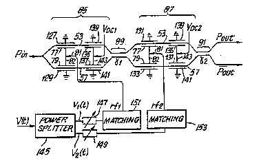
a modulating voltage V(t) is provided to a power splitter 145,
such as a Y-branch power splitter, for splitting the input signal
V(t~ into two substantially equal rf signals V~(t) and V2(t), for
connection to the input terminals of variable rf attenuators 147
and 149, respectively. The output of variable attenuator 147 is
connected to the input of impedance matching circuitry 151, the
output of the latter providing rf signal rfl to electrode 81 of
phase modulator 85. Similarly, impedance matching circuitry 153
is included for receiving the output signal from attenuator 149
for providing rf modulating signal rf2 to electrode 81 of phase
modulator 87. The modulator structure of Figure 14 is a
practical implementation with low switching or modulating
voltage. Due to fabrication inaccuracies, the coupling angle ~
for couplers 89 and 91, respectively, may devia~e from intended
design values. With the embodiment of Figure 14, errors due to
such fabrication inaccuracies are compensated for by using
variable attenuators 147 and 149 to adjust the amplitudes of the
rf signals applied to matching circuits 151 and 153. Also,
fabrication errors may cause asymmetric phase modulation, which
is compensated for in this embodiment by adjusting the levels of
the dc-bias voltages V~ and VD~ through use of adjustable DC
voltage supplies (not shown), for example. Further note that the
27
., ., .. , , , ., . . . . . . . . - - . .. , , .. , - . . ~ . .
W093~23789 2 1 3 6 Z 2 9 ! ; PCTJUS93/03~
external matching circuitry 151 and 153 provides for insuring a
flat and equal frequency response for rf~input signals rfl and
rf2, by phase modulators 85 and 87, respectively. Note further
that the le~el of the light input signal P~ is typically in the
range of 10 to 100 millivolts, and the rf modulating signal V(t),
is typically is 0 to 10 dBm for a cable TV signal, for example.
In Figure 15, a linearized modulator prototype design
is shown, that is related to the simplified configuration of the
modulator of Figure 14. Similar items between the two figures
are indicated by the same reference designation.
As shown in Figure 15, the linearized modulator 84
includes an input waveguide in the form of a Y-splitter 172, for
receiving and splitting a light input signal P~, and guiding the
I split light signals into elongated waveguides 53 and 57,
respectively, of phase modulator 85. The fixed coupler 89
! couples the output light signals from waveguides 53 and 57 to the
like waveguides 53 and 57, respectively, of phase modulator 87.
The output light signals from phase modulator 87 are coupled by
fixed coupler 91 to output waveguides 201 and 203, respectively,
for providing complementary P~l and P~, modulated and linearized
lighk output signals, respectively. In this configuration,
ground plane or RFI electrodes 173, 175, and 177, are generally
rectangular in shape, successively juxtaposed from one another,
and overlie the elongated parallel waveguides 53 and 57, of the
associated phase modulators 85, 87, respectively, as shown. The
parallel and opposing longer sides of each of the RFI electrodes
173, 175, 177 ar~ positioned to be parallel to the waveguides 53
28
~~j W093/23789 2 1 3 6 2 2 9 PCT~US93/03~0(.
and 57, and on the outside thereof, in this example. Centrally
located openings 174, 187, 189, are formed in a llke elongated
side of each one of the RFI electrodes 173, 175, 177,
respectively, for permitting the leg portions of T-shaped
electrodes 181, 185, and 193, respectively, to pass therethrough.
As shown, for each of the T-shaped electrodes 181, 185, 193, the
top associated narrow electrode portions are positioned parallel
to and between waveguides 53 and 57, and within the rectangular
area formed by the RFI electrodes 173, 175, and 177, as shown.
The T-shaped electrodes 181, 185, and 193, ha~e their leg
portions terminating at and connected to connection or terminals
pads 179, 183 and 191, respectively.
For each of the phase modulators 85 and 87, the RFI
electrodes 173, 175, and 177, are connected to a source of
reference potential, ground in this example. Phase modulator
85 has connection or terminal pads 179 and 183 connected to
impedance matching circuit 151 for receiving a portion of a
modulating signal rfl. Terminal pad 191 is connected to receive
the DC bias voltage V~. Similarly, phase modulator 87 has
terminal pads 179 and 183 connected to impedance matching circuit
153 for receiving an rf modulating signal rf2, and terminal pad
191 is connected to receive DC bias voltage V~.
Impedance matching circuits 151 and 153 include three
inductors 165, 167 and 169, connected in series with a load
resistor 171. One end of the load resistor 171 is connected to
a source of reference potential, ground in this example. The
other end of inductor 165 of matching circuit 151 is connected
29
2136229
W093/23789 PCT/~IS93/03~(~f.
to receive modulating signal rfl. Similarly, the other end of
inductor 165 of matching circuit 153 is~connected to receive
another modulating signal rf2. In matching circuit 151, the
common connection between inductors 165 and 167 is connected to
terminal pad 17g of modulator stage 85, and the connection
between inductors 167 and 169 is connected to terminal pad 183
of modulator stage ~5. In matching circuit 153, the common
connection between inductors 165 and 167 is connected to terminal
pad 179 of modulator stage 87, and the common connection between
inductors 167 and 169 is connected to terminal pad 183 of
modulation stage 87.
RF input ignal V(t) is connected to a power splitter
145. One output signal from splitter 145 provides modulating
signal rfl to matching circuit 151. The other output signal from
power splitter 145 is connected through an adjustable delay
circuit 161 to adjustable amplitude control circuit 163. The
output signal from the adjustable amplitude control circuit 163
provides modulating signal rf2 to matching circuit 153.
In the linearized modulator of Figure 15, the RFI
elactrodes 173 and 175 are, in this example, divided into two
separate configurations to facilitate electrical or impedance
matching to the characteristic impedance of load resistor 171 in
the associated matching circuit 151 or 153. Also in this manner,
resistive losses in the electrode structures for electrodes 173
and 175 are minimized. Alternatively, but less preferred, a
single electrode structure could be utilized in place of
electrodes 173 and 175 in the form of a traveling wave
W093/~3789 2 1 3 6 2 2 g PCTt~lS93~03~
configuration. However, for the latter configuration, thicker
electrodes would be required relative to the preferred
configuration, in order to reduce electrode resistive losses.
I Also, for the latter configuration, an impedance transformer or
! 5 additional resistor may be required in each of the impedance
matching circuits 151 and 153. Note also that to obtain the
desired characteristic impedance for the matching circuits 151
and 153, the value of inductor 167 is typically twice the
inductance of inductors 165 and 169, with the values being chosen
to match the capacitance of the electrodes of phase modulators
85 and 87, respectively, for obtaining the correct characteristic
impedance for matching circuits 151 and 153, respectively.
Inductors 165, 167, 169 can be provided by high-impedance
transmission lines stubs connected with bond wires in a printed
circuit ~oard layout, for example.
The power splitter 145 can be provided by a wide-band
hybrid transformer, or in the application of in-phase feeding of
the rf electrodes 181 and 183, respectively, a resistive power
splitting network can be used. Adjustable delay circuit 161 can
be provided by an all pass discrete component network with
variable components, or by a folded transmission line with
adjustable band connections. The adjustable amplitude circuit
163 can be provided by any commonly available variable
attenuator, or from a resistive network with variable components,
as would be known to one of skill in the art.
Although various embodlments of the invention have been
illustrated and described herein, they are not meant to be
31
_ ... .... . .. ..
9~ P 7439 ~136229
limitingO Those skilled in the art may recognize
modifications to these various embodiments, which
modifications are meant to be covered by the
scope of the appended claims.
All~tENDED SHE~T