Note : Les descriptions sont présentées dans la langue officielle dans laquelle elles ont été soumises.
ATTORNEY'~ DocKET ~ PATENT APPLICATION
~ TI-17853
(32350-0858)
DIRECT VIEW DEFORMABLE MIRROR DEVICE
TECHNICAL FIELD OF THE INVENTION
This invention relates to image display systems, and
more particularly to a deformable mirror device that
provides a direct view image.
ATTORNEY'S ~OcKET ~ t ~ 7 ~ ~ ~ PATENT APPLICATION
_ TI-17853 ~ ~
BACKGROUND OF THE INVENTION
Real-time display systems based on spatial light
modulators (SLMs) are increasingly being used as an
alternative to display systems using cathode ray tubes
(CRTs). SLM systems provide high resolution displays
without the bulk and power consumption of a CRT system.
Digital micromirror devices (DMDs) are a type of SLM,
and may be used in display applications. A DMD has an
array of micro-mechanical pixel elements, each having a
mirror and a memory cell. Each pixel element is
individually addressable by electronic data. Depending on
the state of its addressing signal, each mirror is tilted
so that it either does or does not reflect light to the
image plane, i.e., so that it is on or off. The proportion
of time during each video frame that a mirror is in an on
state determines shades of gray -- from black for zero on
time to white for 100 percent on time.
Existing DMD display systems are projection systems.
Light from the on mirrors passes through a projection lens
and creates images on a large screen. Light from the off
mirrors is reflected away from the projection lens and
trapped. Color may be added in two ways, by a color wheel
or by a three-DMD configuration.
DMDs may be fabricated using semiconductor fabrication
techniques. To fabricate a DMD, standard CMOS processing
steps are completed for a static RAM, which comprises the
memory cells, and for address electrodes. Then, a "roof"
of tilting mirrors is fabricated over the memory and
address circuit. The height of this superstructure is
enough to allow the mirrors to tilt plus and minus 10
degrees or so about a torsion axis.
The display optics for viewing the image generated by
the DMD is easily implemented for projection viewing. For
example, the DMD may be coupled with dark-field projection
optics. Here, a bright light source is directed to the
_ TI-17853 2 13 7 ~ 5 8 PATENT APPLICATION
chip at an angle to its surface. Mirrors tilted to an on
position reflect the incoming light through a projection
lens and onto a screen. Mirrors tilted to an off position
reflect the incoming light so as to miss the projection
lens.
ATTORNEY'S DOCKET ~137Q5~ PATENT APPLICATION
._ TI-17853
SUMMARY OF THE INVENTION
A first aspect of the invention is a raceplate for a
direct view display system, which provides images reflected
from a digital micromirror device (DMD) having mirror
elements that are tilted to on or off positions. The
faceplate has a number of optical fibers, attached toqether
such that they are parallel and closely spaced. Upper and
lower end surfaces of the fibers are at the upper and lower
surfaces, respectively, of the faceplate. These end
surfaces are angled with respect to the axis of the optical
fibers, at an angle that is determined by the on tilt angle
of the mirror elements. The faceplate is spaced above the
surface of the DMD and permits ambient light to travel down
the fibers and be reflected back up by the on mirror
elements.
A te~hnical advantage of the invention is that it
permits a DMD-generated image to be directly viewed without
a bulky optical system. The direct view system is
inexpensive and compact. It is suitable for head or wrist
mounted, or other small displays.
TI-17853 2 13 7 ~ ~ 8 PATENT APPLICATION
BRIEF DESCRIPTION OF THE DRAWINGS
Figure l is a cross sectional view of a direct view
display system, which uses a DMD to generate an image from
image data.
Figure 2 is a perspective view of a single mirror
element and an associated optical fiber of a direct view
DMD.
Figure 3 is a cross sectional view of the display
system of Figure l, with the mirror elements in an on
position to receive and reflect incident light.
Figure 4 illustrates how the faceplate for the display
system may be made from a bundle of optical fibers.
Figures 5 - 7 illustrate relative sizes of a mirror~s
surface and the diameter of the optical fibers of the
faceplate.
Figure 8 illustrates a direct view display system with
an internal light source.
Figure 9 illustrates a faceplate having a transparent
color filter.
ATTORNEY'S ~OCRET 2 ~ 3 7 ~ ~ 8 PATENT APPLICATION
TI-17853
DETAILED DESCRIPTION OF THE INVENTION
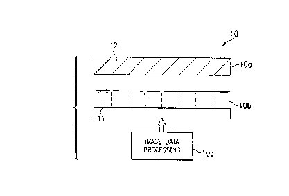
Figure 1 is a cross sectional view of a direct view
display system 10, which uses a digital mi~-o irror device
(DMD) 10b to generate an image from data provided by image
data processing unit 10c. A faceplate 10a directs ambient
light to the surface of the DMD and directs the image back
to the viewer.
DMD 10b is an array of mirror elements 11, which tilt
in accordance with the state of data received from image
data proces6ing unit 10c. Each mirror element 11 has three
states. Its mirror may tilt in either of two directions,
as indicated by the dotted lines, or it may have a flat
position, in which the mirrors are parked when the DMD is
not in use.
Faceplate 10a is attached to DMD 10b and spaced from
the top surface of DMD 10b. The spacing between the top
surface of DMD 10b and the bottom surface of faceplate 10a
is enough to permit the tilting action of the mirror
elements 11 of DMD 10b.
Faceplate 10a is a set of optical fibers 12, which are
parallel to each other and positioned so that their end
surfaces are at the top and lower surface of faceplate 10a,
respectively. These end surfaces are angled with respect
to the axis of the fibers 12, each angle being the same.
As explained below in connection with Figure 3, this angle
is determined by the on tilt position of each mirror
element 11.
Fibers 12 are attached to each other, which may be
accomplished by any one of a n-~mher of means. For example,
fibers 12 may be attached by means of adhesive or by means
of a template having vias through which fibers are
inserted. A common means for manufacturing a bundle of
optical fibers is to adhere them to each other by means of
a glass frit material that serves as a type of adhesive.
- ATTORNEY'S DOCKET 2 ~ 3 7 ~ 5 8 PATENT APPLIC~TION
-- TI-178S3
In the example of this description, fibers 12 are
attached so that they are immediately adjacent to each
other. In other embodiments, fibers 12 could be slightly
spaced apart, but in general, fibers 12 are densely packed.
Typically, as shown in Figure 1, the length of optical
fibers 12 is short relative to the area of faceplate 10a.
In Figure 1, there a one-to-one correspondence of
mirror elements 11 to optical fibers 12. However, in
different embodiments, more than one pixel element 11 may
share a fiber 12, or a pixel element 11 may have more than
one fiber 12. As explained below in connection with
Figures 5 - 7, the number of fibers 12 relative to the
number of mirror elements 11 is related to the resolution
of display 10.
Image data processing system 10c receives analog or
digital video data to be displayed on DMD 10b. If the data
is analog, processing system 10c converts the data to
digital form. It performs other operations such as de-
gamma correction, color conversion, and progressive
scanninq, and other image processing tasks. These tasks
may be implemented with logic circuits, with a processor
executing storing instructions, or with some combination or
hybrid of both types of processors. Processing system 10c
includes a display memory for buffering frames of data in
a "bit-plane format", in which each frame of pixel values
are delivered to the DMD 10b one bit per pixel at a time.
Further details about an exemplary image data processing
system 10c for use with a DMD 10b, are set out in U.S.
Patent No. 5,079,544, entitled "Standard Independent
Digitized Video System", U.S. Serial No. (Atty
Dkt No. TI-17855), entitled "Digital Television System",
U.S. Serial No. 07/678,761, entitled "DMD Architecture and
Timing for Use in a Pulse-Width Modulated Display System";
U.S. Serial No. 07/809,816, entitled "White Light Enhanced
Color Field Sequential Projection"; and U.S. Serial No.
ATTORNEY'S ~OCXET ~ ~ 3 7 n 5 ~ PATENT APPLICATION
- TI-17853
(Atty Dkt No. TI-17671), entitled "DMD Display
System". Each of these patents and patent applications are
assigned to Texas Instruments Incorporated, and each is
incorporated by reference herein.
Figure 2 is a perspective view of a single mirror
element 11 having an associated optical fiber 12. Whereas
Figure 1 is a side view showing the tilt angles of each
mirror element 11, Figure 2 is a front view. In Figure 2,
mirror element 11 is shown in its flat position but it
could tilt up or down as indicated by the arrows.
A typical mirror element 11 is square, with 16
micrometers on a side. Mirror elements 11 may be spaced as
closely as 1 micrometer apart. A typical DMD lOb might
have thousands of mirror elements 11. Thus, for example,
where DMD lOa is a square array of 1000 x 1000 mirror
elements 11, the dimensions of faceplate lOa would be in
the order of 17,000 x 17,000 micrometers.
The array of mirror elements 11 is fabricated on a
silicon substrate 21 using semiconductor fabrication
te~hni ques. Each mirror elements 11 is in electrical
communication with a memory cell 22 of a static RAM.
Depending on the particular addressing scheme to be
implemented, each mirror element 11 might have its own
memory cell 22, or several mirror elements 11 might share
a memory cell 22. Directly over memory cell 22 is an
addressing layer, having two landing electrodes 23 and two
address electrodes 24. Only one landing electrode i8
visible in Figure 2; the two electrodes 23 are under
opposing corners of the mirror 25. Mirror 25 is above
electrodes 23 and 24, supported by hinges 26 attached
support posts 27.
To fabricate a DMD, standard processing steps are used
to create the layer of static RAM cells 22 on substrate 21.
Typically, the RAM cells 22 are made in accordance with
35 CMOS processing. The electrodes 23 and 24 may be
ATTORNEY'S DOCKET ~ ~ ~ 7 ~ 58 PATENT APPLICATION
fabricated with conventional metal lithography. At the
next processing phase, the wafer is coated with a polymer
spacer layer. Vias are etched through the polymer layer to
contact sites, on which are fabricated the support posts
27. Next, a thin aluminum layer (for hinges 26) and a
thicker aluminum mirror layer (for mirrors 25) are
deposited, patterned, and etched. A plasma etch removes
what is left of the polymer layer, leaving the mirrors 25
suspended above the electrodes 23 and 24 by the hinges Z6
attached to the support posts 27. I n o p e r a t i o n ,
electrostatic forces, based on the data in memory cell 22,
as applied to address electrodes 23 and 24, cause mirror 25
to tilt. While tilted, the surface of mirror 25 is flat
and the hinges 26 twist in torsion.
Further details about the structure, operation, and
fabrication of an exemplary DMD are set out in U.S. Patent
~o. 4,956,619, entitled "Spatial Light Modulator", and
incorporated herein by reference.
Figure 3 illustrates how the optical fibers 12 of
faceplate lOa are slanted at an angle that is determined by
the on tilt angle of mirror elements 11. If the tilt angle
is e, the angle at which fibers 12 are slanted is 90 - e
degrees. This angle is referred to herein as the "bias
angle" of the fibers 12. The bias angle permits light to
travel down the fibers 12 and be reflected by the mirrors
25 that are on. Mirrors that are tilted to an off position
will reflect light out of the acceptance angle of the
fibers 12. The light reflected by the off mirror elements
11 is absorbed at the back of faceplate lOa. The viewer
will see the on mirror elements 11 as light and the off
mirror elements 11 as dark.
Figure 4 illustrates how faceplate lOa may be made by
slicing a bundle of optical fibers 12'. Figure 4 is
greatly simplified -- where there is a one-to-one
correspondence between fibers 12 and mirror elements 11,
ATTORNEY'S DOCKET 2 1 ~ 7 Q ~ 8 PATENT APPLICATION
- TI-17853
faceplate lOa would be made from as many fibers 12' as
there are mirror elements 11, and the diameter of each
fiber 12' would be approximately same as the side dimension
of each mirror element 11. However, as explained below,
the diameter of fibers 12 is a matter of desired
resolution.
Many optical fibers 12' are drawn into a bundle and a
portion of the bundle is sliced off. For mirror elements
11 having a 10 degree on tilt position, the bundle is
sliced 80 degrees (90 - 10 degrees) off-axis. For mirror
elements 11 having other degrees of on tilt positions,
fibers 12' would be sliced at a corresponding angle.
Figures S - 7 illustrate how the relationship between
the end surface area of fibers 12 and the surface area of
mirrors 11 affects the resolution of display 10. Figures
5 - 7 are top plan views, representing the view down fibers
12 onto the surfaces of mirror elements 11. Each fiber 12
has an "acceptance area", determined by its diameter, D.
In Figure 5, as in Figures 1 - 4, the acceptance area
of fiber 12 "matches" the surface area of mirror element
11, in the sense that the diameter of fiber 12, D, is
approximately the same as the side dimension, L, of mirror
element 11. For this embodiment of faceplate lOa, the best
resolution is achieved if each fiber 12 is centered over
its corresponding mirror element 11, as illustrated.
Various te~hniques can be used when attaching faceplate lOa
over DMD lOb to ensure proper alignment.
In Figure 6, each mirror element 11 has four fibers
12. This embodiment reduces the need to ensure alignment
of faceplate lOa to DMD lOb. For example, if the four
fibers 12 were shifted to one direction or another, with
respect to the surface of mirror element 11, mirror element
11 would continue to receive and reflect all light from two
fibers 12. The greater the number of fibers per mirror
- ATTORNEY'S ~OCKET 7 ~ ~ 7 ~ ~ ~ PATENT APPLICATION
- TI-17853
11
element 11, the less critical the alignment of fibers 12 to
mirror elements 11.
In Figure 7, the acceptance area of each fiber 12 is
greater than the surface area of mirror element 11. In
this type of embodiment, display 10 operates with a
corresponding decrease in resolution. For example, if a
single fiber 12 were placed above a set of four mirror
elements 11, the on and off positions of those four mirror
elements 11 would determine the portion of the image
reflected back to the viewer. However, an advantage of
this emho~i -nt is that the on and off times of each mirror
elements 11 of the set of four mirror elements 11 can be
controlled to provide a greyscale value under their fiber
12.
Figure 8 illustrates how a light source 81 may be
placed at one side of the space between faceplate 10a and
DMD 10b. This permits display 10 to generate images when
there is no ambient light to be carried to the surface of
DMD 10b by fibers 12. A control unit 82 permits a user to
switch light source 81 on or off and provides any power
that might be required. As indicated, light source 81 is
positioned to a side of DMD 10b that corresponds to the
direction of the "on" tilt position. If light source 81
directs light to the bottom surface of faceplate 10a, the
end surfaces of fibers 12 will disperse the light toward
the reflective surface of DMD 10b. Light source 81 may be
one or more light emitting diodes (LEDs) or some other
a~G~riate source of light.
Light source 81 may be a single white light source for
black and white images. For greyscale images, processing
unit 10c can implement pulse width modulation techniques,
so as to control the length of time during each frame
period that a mirror element 11 is on or off.
Or, as shown in Figure 8, for color images, light
source 81 may be a set of three light sources, red, green,
- ATTORNEY'S ~OCKET 2 ~1 3 7 ~ 5 ~ PATENT APPLICATION
TI-17853
12
and blue. Each mirror element 11 receives data for each
color sequentially. The different color sources are turned
on and off, sequentially, in synchronization with the data
being receiving by the mirror elements.
Figure 9 illustrates an alternative embodiment of
faceplate lOa, for providing color images. In this
embodiment, faceplate lOa has a transparent color filter 91
covering the upper end surfaces of fibers 12. Color filter
91 has alternately strips of red, green, and blue material.
The incident light is filtered by these strips as it passes
through color filter 91, thereby producing color images.
Alternatively. color filter 91 could cover the bottom end
surfaces of fibers 12. Also, instead of strips of
differently colored material,filter 91 could be made from
triads of red, green, and blue squares or other polygon
shaped areas, of material. Ideally, the size of these
stripes or shapes is sufficiently small to provide one
color for each mirror element 11, but other relative sizes
are possible.
Other Embodiments
Although the invention has been described with
reference to specific embodiments, this description is not
meant to be construed in a limiting sense. Various
modifications of the disclosed embodiments, as well as
alternative embodiments, will be apparent to persons
skilled in the art. It is, therefore, contemplated that
the appended claims will cover all modifications that fall
within the true scope of the invention.