Note : Les descriptions sont présentées dans la langue officielle dans laquelle elles ont été soumises.
!
`: ~093/26140 2~37~89 PCT/US93/0~67
ELECTRODET,ESS DISCHARGE LAMP CONTAINI~G
PU5H-PULL CLASS E AMPLIFIER AND BIFIL~R COIL
FIELD OF THE INVENTION
This invention relates to electrodeless discharge
lamps and in particular to an arrangement for a highly
efficient electrodeless discharge lamp which generate's
l0 acceptable levels of radio frequency interference.
BACKGROUND OF-THE-INvENTIoN
Electrodeless discharge lamps operate by using an
induction coil to couple electromagnetic energy to a gas
mixture, typically a metal vapor and an inert gas, which
lS is enclosed in a sealed vessel. An oscillator is used to
generate a high frequency signal which is amplified and
delivered to the induction coil. Generally speaking, the
lamp operates in two stages. In the start-up stage, the
induction coil produces an electric field which ionizes
20 some of ~he gaseous molecules, creating ions which in turn
collide with other molecules, thereby producing further
ions. This process continues until ~he steady-state stage
is reached wherein a plasma of circulating charged
particles is maintained, primarily by the magnetic field
25 emanating from the induction coil. The stream of charged
particles excites the metal vapor atoms, producing
radiation, primarily in the W spectrum, which impinges on
a layer of phosphors which coats the walls of the vessel.
As a result, the phosphors are excited and produce visible
30 light.
This type of lamp is known as an electrodeless
fluorescent lamp. Other types of electrodeless discharge
,, , . , ~ . .
W0g3/26l40 Z 1 3 7~ 8 9 - 2 - PCT/US93/0~67
lamps produce visible light directly from the gas
contained in the sealed vessel.
lectrodeless discharge lamps, and in particular
electrodeless fluorescent lamps, are much more efficient
S and long-lived than incandescent lamps. An electrodeless
fluorescent lamp, for example, has a luminous efficacy of
60-80 lumens/watt, whereas tungsten incandescent lamps
typically have a luminous efficacy of only 15-17
lumens/watt. Electrodeless discharge lamps accordingly
10 offer the prospect of very significant energy savings.
The development of this technology has been limited,
however, by several problems, the foremost of these being
the generation of radio frequency interference tRFI). The
induction coil acts as an antenna. Even if the lamp
15 operates at frequencies which are approved by the FCC
(e.g., 6.78 or 13.56 MHz), the lamp typically generates
harmonics of the fundamental frequancy which are not
within approved wavebands. Another problem has been to
minimize losses which occur in the amplification of the
20 high-frequency signal before it is delivered to the
induction coil. These problems have been particularly
troublesome because the apparatus used to solve them must
fit within the confines of an electric light bulb and must
not unduly raise the costs of manufacturing the light
25 bulb.
Class E amplifiers are known to be highly efficient,
and their use in an electrodeless discharge lamp is
described in U.S. Patent No. 4,245,178 to Justice. The
theory underlying Class E amplifiers is described in U.S.
30 Patent No. 3,919,656 to Sokal et al., which is
incorporated herein by reference. The Justioe patent,
however, describes only a single-ended Class E amplifier
an offers no solution to the RFI problem. The single-
ended Class E amplifier produces a half sine wave which is
35 rich in harmonics. Moreover, Justice relies on a self-
oscillating circuit, containing a feedback winding on a
toroidal core, to provide the operational frequency of the
"
. ~. . - . .
- 2~372~3~ -
093126140 . PCT/US93/0~67 .
_ 3 _
lamp. This arrangement does not yield a stable frequency.
The principles of this invention offer a cost- .
effective solution to both the efficiency and RFI ~ -
problems. .
5 SU~MARY OF THE INVENTION
In accordance with this invention, a push-pull Class
E amplifier, containing two switching elements, i~ used to
amplify the high-frequency signal in an electrodeless
discharge lamp. The push-pull amplifier is preferably
lO balanced and produces a modified full sine wave which has
a far lower ~armonic content than a half sine wave.
An induction coil, which may be center-tapped and
which to~ether with the plasma constitutes the load, i.s
directly coupled to a DC source. .apacitors are connected
l5 in parallel with the induction coil. The values of these
capacitors are hosen to provide re~onance with the
induction coil at a frequency lower than the operating
frequency, and thus the parallel combination looks like a
capacitor at the operating frequency.
In a preferred embodiment, an inductor is connected
in series with each of the switching elements (typically
field effect transi.stors (FETs~). The inductors combine
with the coil/capacitor combinations to provide a damped
series resonant circuit which substantially reduces the
25 energy losses which occur during the switching of the FETs
by causing the overall circuit to operate in a Class E
mode. The inductors are also used to match the impedance
of the coil load to that of the switching elements. The
capaci~ors, in conjunction with the inductors, form a low-
30 pass filter which substantially reduces the harmonicswhich are delivered to t~e coil.
According to another aspect of the invention a
bifilar or other type of multifilar induction coil is
used, preferably a center-tapped coil. A coaxial coil may
35 also be used. The multifilar coil causes the electric
field dipoles between adjacent windings of the coil to
~ ~`, ?`
U'093/~6140 PCT/VS93/0~67
~ 4 -
cancel out at distances removed from the coil, thereby
substantially rPducing the RFI problem.
DESCR~PTION OF T~NGS
Figure l illustrates a block diagram of an
5 electrodeless discharge lamp.
Figure 2A illustrates a circuit diagram of a
preferred embodiment of an amplifier in accordance with
the invention.
Figures 2B, 2C and 2D illustrate circuit diagrams of
l0 alternative embodiments in accordance with the invention.
Figure 3 illustrates a waveform produced by the
amplifier of this invention.
Figure 4 illustrates a circuit diagram of a frequency
trap which may be used in conjunction with the invention.
Figure 5A illustrates a bifilar coil in accordance
with another aspect of this invention. Figure 5B
illustrates a schematic diagram of the bifilar coil.
Figure 6 illustrates ~ cross-sectional view of the
wires in he bifilar coil showing the electric field
20 adjacent the wires.
Figure 7A illustrates schematically a center-tapped
bifilar coil.
Figure 7B illustrates a center-tapped quadrifilar
coil.
Figures 8A, 8B and 8C illustrate the common mode
voltage associated with a single ended coil, a center
tapped coil and a bifilar coil, respectively.
Figure 9 illustrates an embodiment including a
coaxial coil.
Figures lOA and lOB illustrate embodiments including
a multifilar coil and a single-ended driving amplifier.
DESCRIPTION OF ~HE INV~N~I,ON
A general block diagram of an electrodeless discharge
lamp lO is illustrated in Figure l. A power supply ll
35 rectifies the AC voltage from the power mains and supplies
27 37289
~93/26140 ; PCT/US93/0~7
DC power to an oscillator 12 and an amplifier 13.
Qscillator 12 is typically crystal driven. The amplified
output of amplifier 13 is delivered to a cylindrical
induction coil 14 which is situated in a cavity protruding
5 into a sealed vessel ~5. Sealed vessel 15 contains a
mixture of a metal vapor, typically mercury, and a rare
gas. When the high-frequency signal produced by
oscillator 12 and amplified by amplifier 13 is delivered
to induction coil 14, electric and magnetic fields are s
10 created inside vessel 15, and a plasma of charged
particles is formed, as described above. The circulating
charged particles collide with the metal vapor atoms,
exciting them and causing them to emit radiation. In a
fluorescent discharge lamp, the radiation is generally in
lS the W spectrum and impinges on phosphors which are coated
on the inside of ~essel 15. This excites the phosphors
which in turn emit visible radiation. In other types of
electrodeless discharge lamps, visible light is emitted
directly by the gaseous atoms. The principles of this
20 invention are applicable to both types of electrodeless
discharge lamps. Moreover, while induction coil 14 is
illustrated as being corele~s, the principles of this
invention also apply to induction coils having a magnetic
core.
As described above, two of the main problems in
developing this technology have been in minimizing the
transmission of radiation from coil 14 into the
surrounding environment, including both the fundamental
and harmonics of the frequency at which oscillator 12
30 operates, and minimizing losses in the transfer of power
from power supply 11 to induction coil 14.
Both of these problems are alleviated in the
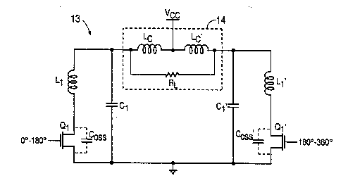
embodiment of amplifier 13 illustrated in Figure 2A.
Amplifier 13 is shown as a Class E amplifier of the push-
~ 35 pull variety. Induction coil 14 is center-tapped and is
;! represented schematically as two inductors LC and LC' with
an equivalent parallel resistor RL representing the loading
/
?~
.r', .` t ~ S . ;~
WO93/26140 2~37Z89 PCT/USg3/0~67 ~ '
- 6 -
effect of the plasma. Amplifier 13 includes switching
field ~ffect transistors (FETs) Q~ and Q~l, each of which
operates out of phase with the other (i.e., one of the
FETs is turned of f when the other FET is turned on,
5 referred to herein as the "push-pull mode") and has a duty
cycle of 50%. The duty cycles of FETs Q~ and Q,' may be ~ ¦
reduced, however, without departing from the principles of
this invention. Inductors L~ and L~' are connected in
series with induction coil 14, and capacitors Cl and C~ '
10 are interposed between the respective sides of induction
coil 14 and ground. FETs Ql and Q~' are shown as having
inharent capacitances C~, and C~,', respectiYely.
The preferred embodiment is completely balanced,
which means that Q, and Ql' are identical FETs, and
15 L~ = L~', C~ = C~', and LC = Lc'-
Several general o~servations wîll assist inunderstanding the design and operation of the circuit
illustrated in Figure 2. The components which represent
cen~er-tapped induction coil 14 (Ic~ Lc' and RL), together
20 with capacitors Cl and Cl ', act as a capacitance at the
operating frequency. This capacitive unit operates in
conjunction with inductors L~ and Ll', respectively, to
form a damped resonant circuit which minimizes the
switching power losses in FETs Ql and Ql' in accordance
~5 with the teachi~gs of the above-referenced U.S. Patent No.
3,919,656 to Sokal et al. These relationships assure that
the voltage across FETs Ql and Ql' is substantially equal
to zero (actually VDS(~) when they turn off, and that the
voltage across and current through FETs Ql and Ql' are
30 substantially zero when they turn on. As described in the
Sokal et al. patent and elsewhere, satisfaction of these
conditions (referred to herein as the "Class E
conditions") minimizes the power losses (voltage x
current) in the intervals during which FETs Ql and Ql' are
35 switching between their on and off states.
Inductors L~ and L,' provide impedance matching and
capacitors Cl and C~' act as low-pass filters, minimizing
Z~372~39
.
; V093J26140 ~q ~ ~C~/US93/0~67
- 7 -
harmonics of the fundamental frequency (determined by
oscillator 12) from reaching induction coil 14.
The design of amplifier 13 involves finding the
optimal comp~omise among several competing factors. The
5 following describes a general methodology for this
process.
1. The inductance and load of induction coil 14 are
defined for the situation in which it is operating in an
energized electrodeless discharge lamp.
2. FETs Q, and Ql' are selected to have output
capacitances and breakdown voltages consistent with the
power output requirements of the amplifier.
3. The capacitance (C~) required to produce
resonance with induction coil 14 at the desired operating
15 frequency is calculated.
4. The values of the series inductors L~ and L~' are
calculated such that they provide the impedance
~ransformations necessary to match the impedance of
induction coil 14 to the respective impedances of FETs Q~
20 and Ql'.
S. The values of capacitors C~ and C~' are
calculated to provide a series resonance at`the desired
operating frequency wîth one of FETs Ql and Q~' turned on.
6. Using the calculated values, the performance of
25 the damped resonant circuit is simulated on a computer to
obtain the optimal voltage waveform at the drain terminals
of FETs Q~ and Ql', i.e., starting with ~ = 0, when the FET
turns o~f, the voltage at the drain terminals should vary
such that V = 0 and ~V/dt = 0 when the FET turns on.
7. The supply voltage Vcc necessary to provide the
desired output power is selected.
8. A breadboard with the component values obtained
from the computer simulation is built and tested and those
values are adjusted as necessary to meet the "Class E
35 conditions", as described above, with a selected
coil/plasma combination.
As will be appreciated by those skilled in the art,
W093/26140 2~289 - 8 - PCT/US93/0~67
elements such as the coil inductance, plasma load
impedance, parasitic coil capacitance, coil and capacitor
tolerances, FET parasitic variations, the
amplitude/impedance of the gate drive signal, and the
5 layout parasitics will all have some impact on the design.
The final solution will be the best compromise taking into
account all of these variables.
An example of the method of constructing an amplifier
in accordance with this invention will now be given. In
10 the example, it is assumed that Lc = Lc' = l.15~H,
RL = 4Xn, the coupling factor K - 0.9, and loaded Q ^' lO.
Q~ and Q1' are FETs with an inherent capacitance C~ 40pF
and a breakdown voltage Vp - 200V. The lamp will operate
at fO = 13.56 MHz.
The power output PO is governed by the following
relationship.
PO - 0.8 CO~ Vp2 f~
which yields PO ~ 18 Watts.
The capacitance Cz required to resonate with the
20 induction coil is defined as follows:
C
x 4~2fo24Lc
C~ ~ 3OpF
To keep the amplifier balanced, one-half of this
capacitance (60p~) should be located on either side of
25 induction coil 14.
Next, the value of the series inductors L~ = L1' is
ca~culated, so as to provide impedance matching ~etween
induction coil 14 and FETs Q~ and Q,', respectively. The
follcwing equation describes this relationship:
RL ~4rC + 2L1~2 VP2
Q2 ~ 4LC ) 2PO
Inserting values for RL~ Q, VP and PO yields:
2~9
,~093/26140 ,!PCT/US93/0~67
_ 9 _
. (4Lc + 2L1)2 25
4LC ~ 2Ll
5
Since ~ = 1.15~H, we get
2LI = 18.~H
5 Ll = 902~H
Accordingly, the condition of impedance matching
yields the series inductance L~ = L~' = 9.2~H.
. Next, Cl = Cl' is calculated so as to provide a series
resonance at fO = 13.56 MHz with one of FETs Q~ or Ql'
10 turned on. (Although the actual frequency of the sleries
resonant circuit should be slightly greater than fO to
eatisfy the Class E conditions, the resulting error can
easily be corrected through simulation and testing.)
fO = -
2~ 2Ll ( 2
. ~ - CX + C05~
15This expression can be solved for Cl.
87~2g~rlcO
Coo
L 1-8~ f LlC099
C~ _ 12OpF
:
The values of Ll and C~ are further refined by
20 simulation and testing, as described above. In most
situations, thQ values obtained fro~ L~ and Cl will assure
that these elements will act as a low pass filter with
regard to harmonics above the fundamental frequency. In
the event that a specific harmonic frequency requires
25 further attenuation, a frequency trap in the form
'2 ~; ~
WO93/26140 PCT/US93/0~67
-- 10 --
illustrated in Figure 4, containing a capacitor C2 and an
inductor ~, may be interconnected betwe~n s~ries inductor
L, and induction coil 14. A similar trap may be connected
between series inductor L~' and induction coil 14.
Unlike a single-ended Class E amplifier such as is
described in the above-referenced U.S. Patent No.
4,245,178 to Justice, the push-pull amplifier of this
invention pro~ides a modified full si~e wave having a ~orm
of the kind generally shown in Figure 3. This waveform
lO has a far lower harmonic content than the half wave output
of a single-ended Class E amplifier.
Figures 2B and 2C illustrate alternative embodiments
of an amplifier in accordance with this invention. The
amplifier shown in Figure 2B is a choke-coupled, DC--
15 connected circuit arrangement, and the amplifier shown in
Fisure 2C is a choke-coupled, AC-connected circuit
arrangement. The induction coil LC may or may not have a
center tap, as illustrated by the hatched line.
Figure 2D illustrates a cascoded circuit arrangement
20 in which the input capacitances of transistors Q~ and Q2
are less and Miller ~eedback effects are minimized and
therefore a smaller driver can be used.
It has been found that the radio frequency
interference (RFI) problem is significantly reduced if the
25 induction coil is bifilar. Figure 5A illustrates a
bifilarly wound induction coil 14. Starting at point a,
th~ coil is wound to point a', where the wire is brought
down on t~e inside of the coil to point b from which it is
wound side-by-side with the first winding up to point b'.
30 This arrangement is illustrated schematically in Figure
. 5B. Each spiral segment of wire between points where the
2 winding begins (e.g., point a) and where it ends (e.g.
point a') is referred to herein as a separate "winding."
Individual passes around the coil support are referred to
35 as "turns".
This technique significantly reduces the electric
field at points distant from the induction coil while
` ~093/26140 ~ PCT/US93/04467
- 11 - I
maintaining a strong electric field at points near the
coil where it is needed to start the ionization process in
~he discharge vessel. The reasons for this, as presently .
understood, are illustrated in Figure 6, which is a cross-
5 sectional view of the coil winding taken through a radial
plan It is assumed that the peak-to-peak voltage is
60V, with ends a and b' oscillating between ~30V and -30V. I
The coil is shown when point a is at +30V and point b' is
at -30V. The turns from point a to point a' are shown as
10 open circles and the turns from point b to point b' are
shown as crossed circles. The voltages shown in Figure 6
are for illustration only, the actual voltage between
points a and b' may be on the order of 200 V to 300 V.
As Figure 6 indicates, the voltage decreases by lOV
15 for each turn from point a, until it reaches oV at point
a'. The voltage at point b is the same as at point a',
and from point b to point b' the voltage decreases lOV for
each turn to -30V at point b'.
A distance dl is shown as the distance between the two
20 windings and the distance d2 is equal to the pitch of each
winding less the distance dl. The result, ~therefore, is a
series of dipoles having a strength equal to the distance
between adjacent wires multiplied by the voltage
difference between the wires. The strength and direction
25 of each dipole is indicated on the right side of Figure 6.
It is apparent that successive dipoles are in opposite
directions and will be equal if:
30dl = 20d2
or
d2 = 1.5d~
For a bifilarly wound coil having n turns in each
half, this expression can be generalized to:
d~
d2 n
WO93/26140 2~3 72 ' `;~ ~"~ PCT/US93/0~67 ~ ,
- 12 -
When this condition is satisfied, the dipol~s
substantially cancel out at points well removed from the
coil (for examplet greater than 10 times the coil length),
while the strength of the electric field at points near
5 the coil is enhanced as compared with the field near a
single-wound coil. For example the dipole between points
a and b in Figure 6 is 30d~, whereas if the coil were
single-wound (8 turns), the strength of the dipole would
be equal to lOdl.
0 The strength of the far electric field of a bifilarly
wound coil having n turns can be approximated as
V 2
Ebjfil~r - sn 2 r~
By comparison, the far field for a simple solenoid is
approximated as:
E _ Vr:s~s
~oleno;d r 2
Accordingly, the suppression of the electric field is .
directly proportional to the number of turns of the
bifilar coil.
Suppression = 10 log~ ~Ebi~ila~] = -20 log10 (2n)
solenoid
The center-tapped bifilar coil illustrated
schematically in Figure 7A is particularly advantageous
for the induction coils illustrated in Figures 2A-2D.
Starting and finishing the winding of the coil at the
center creates a more symmetrical configuration and
25 provides improved far field suppression. Moreover, the
near electric field at the center of the coil is
strengthened by the close proximity of coil windings
having a voltage difference of V~ (+ ~ Vpp to - ~ Vpp).
The principles of this invention extend to multifilar
30 coils having any number of windings located side-by-side
one another. For example, Figure 7B illustrates a
093/26t40 z~3q~89 .~ s ~ PCT/US93/~44~7
- 13 -
quadri~ilar coil.
In addition to the far field cancellation of the
bifilar coil there are other benefits in minimizing the
reradiation of signals by the plasma itself.
Plasma radiation at any frequency can be split into
two components:
~a) Radiation due to the currents and voltages
induced in the plasma by the magnetic coupling.
(b) Common mode voltages induced in the plasma by
lO coupling to the induction coil.
The induced magnetic coupling component can be
reduced by minimizing the harmonic content of the sig~nal
driving the induction coil. The plasma itself does not
create harmonics which are large enough to be considered.
The common mode induced voltage can be analyzed by
assuming capacitive coupling between the induction coil
and the plasma as shown in Figures 8A, 8B and 8C.
A simple analysis reveals that the common mode
voltage VCM for the configurations illustrated in Figures
20 8A, 8B and 8C is approximated by the expressions:
Single ended coil (Fig. 8A):
V~ Z N~'C 1 ¦ 2X1J
Center tapped coil (Fig. 8B):
~t N
~ NC2 2 2
Bifilar coil (Fig. 8C):
N N
~ NC2 2x - 2x ~ 0
where VIN is the rms voltage delivered to the coil, C~
is the capacitance between a singla turn of the coil and
the plasma, C2 is the capacitance between the plasma and
30 ground, N is the total number of turns in the coil, and x
is a variable number.
"r, ?4~
WO93/26140 z~3qz89 PCT/VS93/o~7
- 14 -
As can be seen, a balanced coil configuration has
substanti~lly zero common mode induced voltage in the
plasma while the single ended coil has a finite common
mode value. Any imbalance effects due to physical
5 tolerances, electrical imbalance5, and imbalanced grou~d
effects will have second order effects.
Common mode coupling and hence reradiation and RFI
signals can be minimiæed by
(a) Using multifilar coil configurations to enhance
10 coupling between each half of the coil and to minimize
electrical imbalances.
(b) Improving balance such as using a center feed
and/or quadrifilar coil configuration.
(c) Providing a balanced push-pull drive to the
15 induction coil.
(d) Increasing the value of C2 by an external
~rounded shield, as described in commonly owned
Application Serial No. 07/883,8750, incorporated herein by
reference.
(e) Providing an electrical shield between the
induction coil and the plasma, as described~in commonly
owned Application Serial No. 07/883,972, incorporated
herein by reference.
It may be preferable to use a coaxial cable in some
25 situations, with the central conductor and shield,
r~spectively, being connected in the same manner as the
side-by-side windings described above. Fig. 9 illustrates
schematically one embodiment of such a configuration. In
Figure 9, the solid line represents the central conductor
30 and the hatched line represents the outer shield of the
coaxial cable. A center-tapped configuration is shown,
with the center tap CT being located midway between the
start S and the finish F.
Alternatively, it may be desirable to twist the side-
35 by-side lines in some applications.
A multifilar coil may also be used with a single-
ended driving amplifier, i.e., a single source driving a
J'7~i~
~093~26l40 P~T/US93/~67
- 15 -
load which is connected to the source at one end and
grounded at the other end. In this configuration, the
signal across the multifilar coil energizing the plasma is
balanc d and thus the benefits of low ~FI and low common
5 impedance coupling to the plasma are obtained. Two
possible configurations using a single FET in a Class E
mode are illustrated in Figures lOA and lOB. In both
figures, inductor L~ functions as a seriPs choke for the
induction coil. FET Q~ may advantageously be an IRF 710.
lo The difference between the embodiments shown in Figures
lOA and lOB is that the embodiment of Figure lOA uses a
single tuning capacitor C~ whereas the embodiment of Figure
lOB uses a pair of tuning capacitors C2 and C2'.
Preferably, if the other elements of the circuits are the
15 same, the value of Cl should be equal to one-half the
values of ~ and C2' (which should be equal).
Whîle using a multifilar coil with a single-ended
amplifier will generally not give a signal conversion that
is quite as good as that obtained with a balanced (push-
~0 puIl) drive, the results will nonetheless be superior tothose obtained with a normal single-wound aoil.
The embodiments described above are intended to be
illustrative and not limiting. Accordingly, many other
embodiments will be apparent to those skilled in the art,
25 all of which are within the broad scope of this invention,
which is defined in the following claims. For example,
push-pull Class E amplifiers having circuits different
~rom the one illustrated in Figure 2 may be found suitable
in certain situations.
~, .