Note : Les descriptions sont présentées dans la langue officielle dans laquelle elles ont été soumises.
WO 94/00806 2 1 3 7 3 ~ 6 PCI/US93/04795
VOLTAGE CONTROLLER
F~ELD OF THE TNVENTION
The present invention relates generally to the field of controlling
voltage applied to a load, and more particularly to an apparatus for conserving
5 energy in operating inductive and resistive loads.
BACKGROUND OF THE INVENTION
Energy conservation has becollle a major concern in the design of
electrical circuits and systems. Energy conservation has benefits to the end users
and society as a whole. For example, on the one hand, ~limini.ched use of energy10 lowers operating costs of the system. On the other hand, diminishe~l need forenergy results in ~imini~hed adverse environmental impact such as pollution,
depletion of resources and the like. One example of the need for reduction in
energy consumption lies with the operation of AC motors. The use of such AC
motors has become commonplace. Many ordinary appliances and much of the
15 e luip",ent used in residential as well as in industrial and commercial settings
utilize such motors. These motors are ol~linalily connected to power lines provided
by local utility companies, which can vary substantially in voltage between locales
and over time. Motors typically operate at relatively constant speeds, the speedbeing independent of the applied AC voltage to the motor over a range of
20 operatin~ voltages.
The energy consumption of any load element in an electric circuit,
such as a motor, is determined from the integral over a predetermined period of the
product of the instantaneous AC voltage applied across the load terminals and the
instantaneous AC current through the load. Typical AC line voltages are
25 sinusoidal. It is known that applying a sinusoidal input to an inductive load will
result in both the AC voltage and AC current having the same sine wave shape butwith an offset in time. The time offset between voltage and current is called a
phase shift or phase difference and is typically expressed as an angle. For a
constant voltage and, hence, relatively constant current, the power consumed by a
30 load may be expressed as Vlcos~, where V is the average value of the applied AC
voltage across the load, l is the average value of the AC current through the load
and ~ is the phase difference between the voltage and the current. Cos ~ is
WO 94/00806 , ~, PCI /US93/0479
~3rl 3 ~ ~ 2
sometim~os referred to as the "power factor". Thus, power consumption is relatedto the phase difference between the AC voltage applied to the load and the AC
current through the load. This phase difference is dependent upon the load
condition of the motor. Hence power consumption is dependent upon the load
status of the motor and upon the line voltage applied to the motor.
Most motors are designed to operate adequately at predetel,.,ined
line voltages. Normally, the motor designer must assume that the motor will be
ope.~t~d at the lowest line voltage norm~lly encoun~led. Such a voltage may be
far lower that the normal line voltage available at most locations and at most times.
For example, a load used in a refrigerator must be capable of delivering adequate
power under full load during a "brown-out" condition, i.e., when a utility reduces
line voltage over its entire grid (or portion thereof) in response to unusually high
electrical energy dçm~nfl Changes in line voltage effects both load performance
and energy consumption. While wide variations in line voltage are, thus,
undesirable, such variations are beyond the control of most load designers and
users. It is noted that ordinary line voltage fluctuations will not result in changes
in the phase between the current and the voltage. Prior art energy conserving
systems are responsive to changes in phase but not to fluctuations in line voltage.
Therefore, there is a need for a energy savings system for controlling
the voltage applied to a load which is simple and which is responsive to changes in
line voltage to adjust for such changes.
Accordingly, it is an object of the present invention to provide an
improved load control system for energy savings.
Another object of the invention is to provide an energy savings
system for use with various loads which are simpler in design than the prior art.
These and other objects of the invention will become appale,lt to
those skilled in the art from the following description and accompanying claims
and drawings.
SUMMARY OF THE INVENTION
The present invention comprises an apparatus and method for
controlling the voltage applied to a load. The method includes receiving an AC
line voltage. An operating AC voltage is generated from the AC line voltage and
21373~6
WO 94/00806 PCI`/US93/04795
this operating AC voltage is applied across the load. A measured signal which is a
function of the m~gnitllde of the operating AC voltage is gellcl~ted. The measured
signal is then averaged to generate an average signal representative of the average
value of the measured signal. The op~,laLi-lg AC voltage is continually readjusted
5 in response to changes in the average signal.
An appala~,Js implem~nting the method of the present invention is
also taught. The app~lus includes terminal means for receiving an AC line
voltage, means for ~ ling an Op~laLing AC voltage from the AC line voltage,
connector means for applying the operating AC voltage across the load, and
10 voltage detection means for generating a measured signal which is a function of the
m~nit~1de of said operating AC voltage. Signal averaging means are provided for
gen( ,a~ g an average signal l~sen~ e of the average value of the measured
signal. Finally, the apparatus includes AC voltage modulation means for adjusting
the op~ ing AC voltage in response to the average signal.
In the preferred embodiment of the apparatus of the present
invention, the AC voltage modulation means comprises voltage reduction means forswitching off the line voltage for a portion of each cycle, the length of the portion
being determined by the average value of the measured signal. The voltage
motllll~tion means may comprise a phase control integrated circuit device for
20 controlling a triac. The phase control integrated circuit device is responsive to the
average signal to generate a control signal operative to control a triac to switch off
the line voltage to the load for the portion of each cycle.
BRIEF DESCRIPTION OF THE DRAWINGS
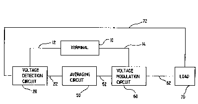
FIG. l is a block diagram showing the major functional components
25 comprising the present invention.
FIG. 2 illustrates an AC voltage modulation means 60 of FIG. l.
FIG. 3 illustrates an plerelled implementation of voltage detection
circuit 20 of FIG. 1.
FIG. 4 illustrates a pref~ d implementation of averaging circuit 50
30 of FIG. 1 utilizing Full Wave Capacitor Coupled Feedback.
FIG. 5 illustrates an alternate implementation of averaging circuit 50
of FIG. 1 utilizing Mean Square Feedback.
~ 3~ 366 PCI`/US93/04795
FIG. 6 illustrates another alternative implement~tion of averaging
circuit 50 of FIG. 1 utilizing Root Mean Square Feedback.
DETAILED DESCRIPTION OF THE INVENTION
While it is known that adjusting the voltage applied to a load may
5 be used to save energy, in order to be practical for most applications, voltage
adjll~tment means must be able to quickly respond to changes in the line voltage.
Available technologies for sensing such changes have not proved practical for
widespread application. In this regard, there is a need for a relatively simple,inexpensive, "foolproof" yet reliable energy saving device. The present invention
10 employs novel means for sensing changes in the AC line voltage thereby allowing
adj-lstn-ent of the voltage to variations in the AC line voltage to save energy.A voltage controller circuit according to the present invention
contains the subcircuits illustrated in block diagram form in FIG. l. The overall
circuit compri~es a feedback loop. In this loop the operating AC voltage across a
15 load 70 is detected by voltage detection circuit 20, which generates a measured
voltage signal representative of the instantaneous m~gnit~lde of the voltage applied
to the load. The measured voltage signal is time averaged in averaging circuit 50
to generate an voltage signal representing the value of the measured signal over at
least one complete cycle. This average signal controls a voltage modulation circuit
20 60, which interrupts application of the AC line voltage to load 70, thus controlling
the average m~gnitllde of the operating AC voltage applied to load 70. Voltage
feedback to voltage modulation circuit 60 responds to changes in the operating and
line voltages.
More specifically. a terminal 10 is provided for directly receiving an
25 AC line voltage from an AC power supply system (not shown), for example, an
ordinary AC outlet. Voltage modulation circuit 60 receives the AC line voltage
from terminal 10 via AC voltage connector 14. Voltage modulation circuit 60
modulates the AC line voltage to generate the operating AC voltage applied to the
load. The AC line voltage is modulated so that the power transmitted to load 70
30 via mocl~ ted AC voltage connector 62 varies in response to a control signal
received by voltage modulation circuit 60 from average signal connector 52. The
method by which the "average" signal is generated is discussed in detail below. It
W O 94/00806 2 1 ~ 7 3 6 6 PC~r/US93/04795
is important to note that the circuit according to the present invention is utilized in
connection with a load 70 which is part of a s~,pa~dt~ device apart from the voltage
controller. It is included in the Figures and rliscuCcion herein to clarify the
relationship between the voltage controller circuit and load 70 to be controlled.
The measu-~,d signal is generated from the voltage applied across
~oad 70 by tr~ncmitting the o~ ting AC voltage across applied AC voltage
connector 72 to voltage detection circuit 20. Voltage detection circuit 20 generates
the measured signal, which is a function of the m~gnitud~ of the opel~illg AC
voltage. In the pl~clled embodiment of the present invention, this representation
is a dirr~l~nce signal belween the AC line voltage and the u~ g AC voltage.
Hence a difference signal between the AC line voltage received over AC line
voltage connector 12 and the operating voltage received over O~.,ld~ g AC voltage
connector 72 is generated and rectified. Those skilled in the art will recognize that
a variety of alternative output signals may be g~,n~l~ted which are also functions of
the operating AC voltage.
The measured signal is then tr~ncmitted via measured signal
connector 22 to averaging circuit 50. Averaging circuit 50 averages the
instantaneous value of the measured signal over at least one cycle, to generate a
voltage representative of the time average of that AC voltage.
The IJlcf~lled embodiment includes an integrator circuit located
within averaging circuit 50 to obtain the average signal from the measured signal.
The average signal thus generated is a signal representative of the rms value of the
measured signal, which is related to the magnitudes of the voltage across the load.
One preferred embodiment of an AC voltage modulation circuit 60
of FIG. 1 according to the present invention is illustrated in FIG. 2. Elements
illustrated in F~G. 1 present in FIG. 2 - 5 are labelled consistently throughout. In
this subcircuit a phase control chip 110 responds to the signal from average signal
connector 52 to control pilot triac 112 and thereby main triac 114. Main triac 114
acts to int~llul)t application of the AC line voltage to load 70 and thereby generate
the operating AC voltage.
W 0 94/00806 C~ ~3~36~ PC~r/US93/04795
The AC line voltage is received at AC voltage modulation circuit 60
via unmo<l~ te~l AC voltage connector lines 14, including an AC line voltage line
("AC hot") and an AC neutral line.
Modulation of the AC Op~,ld~ g voltage of the pl~rell~d
5 embodiment of the present invention is accomplished using pilot triac 112 and
main triac 114. A triac is a well known device whereby small current signals
applied to its gate can control much larger current flows at much higher voltages.
A triac is triggered into conduction by pulses at its gate. In the present circuit a
signal applied at the gate of pilot triac 112 from phase control chip 110 permits a
10 current to flow through triac pilot 112, which is applied to the gate of main triac
114. While it might be possible for a single stage triac to be utili7~tl, a two stage
triac arrangement may allow for control of the relatively large current to a high
power load by a phase control chip which has only a limited capacity to deliver a
gate control current. Therefore this staged triac arrangement permits the output of
15 phase control chip 110 to control the applied AC voltage to load 70 over
modulated AC voltage connector 62.
The voltage applied to the load is controlled by the control signal
pulses received at the gate of pilot triac 112 from phase control chip 110. In one
embodiment of the present invention, a TDA 2088 phase controller chip from
20 Plessey Semiconductors is utilized as phase control chip 110. The TDA 2088 chip
is designed for use with triacs for use in current feedback applications, and isfrequently used for speed control of small universal motors.
Phase control chip 110 requires an applied voltage at voltage input
pin 132 of -12 V and a 0 V reference voltage at 0 V reference pin 142. These
25 voltages are used to power the chip and to generate a -5 V reference voltage at -5
V reference pin 124. This voltage is obtained from the AC line voltage by a
power supply subcircuit, which operates as follows. Resistor 164 and capacitor
162 are connected in series to the AC line voltage on AC line hot line 14 to
provide a filtered voltage to diodes 160 and 158, which permit only the negative30 half cycle of the AC line voltage to pass. Capacitor 178 is provided to smooth the
resulting voltage at voltage input pin 132, and zener diode 180 latches the voltage
at that pin to a value of -12 V.
WO 94/00806 2 1 3 7 3 6 6 PCr/US93/0479~
Phase control chip 110 supplies control signal pulses at triac gate
output pin 134. Phase control chip 110 has an int~rn~l ramp gcncla~or whose value
is co~ ,d to the voltage applied at program input pin 122. When these two
values are equal an output pulse is triggered. The ramp genelalor has two input
5 connections. First, pulse timing resistor input pin 126 is conn~tecl to a -5 V~ ;fe~llce by pulse timing resistor 152. Secondly, pulse timing capacitor input pin
144 is connected to ground by pulse timing c~paritor 148. The values of pulse
timing resistor 152 and pulse timing ca~aci~r 148 are chosen to deflne to slope of
the ramp signal.
In addition to the support Cil-;uiLI y for phase control chip 110
described above, AC voltage mo~ tion circuit 60 is provided with a thermal
switch 150. Thermal switch 150 is connected between ground and average signal
connector 52, which applies the average signal from averaging circuit 50 to
program input pin 122 of phase control chip 110. Thermal switch 150 acts to
15 ground out program input pin 122 if the system overheats. This is a safety feature
which acts to shut off the load in the event of circuit overheating.
Also, resistor 174 and capacitor 176 are provided to act as a
"snubber" network, which enh~nce the ability of main triac 114 to operate with
inductive loads. In the absence of such a snubber network, false firings of the triac
20 might occur with rapidly varying applied voltages. The snubber network acts to
delay the voltage rise to main triac 114 to ensure smooth and correct changes intriac conduction.
FIG. 3 illustrates a plef~-led implementation of voltage detection
circuit 20 of FIG. 1. In this implen,enlalion a difference signal is generated by
25 subtracting the operating AC voltage across load 70 from the AC line voltage. The
~lifr~ nce signal is therefore r~l.,sent~tive of the operating AC voltage and of the
AC line voltage.
In particular, the AC line voltage is received at AC line voltage
connector line 12 and tr~ncmitted through resistor 202 to the non-inverting input of
30 operational amplifier 210. Similarly, the op~ -g AC voltage is received at
applied AC voltage connector line 72 and is tr~ncmittçd through resistor 204 to the
inverting input of operational amplifier 210. Resistor 206 is connected to -5 V and
W O 94/00806 PC~r/US93/04795
b~ ~ 3 1 3 ~ ~ 8
resistor 2 is connected to the output of operational amplifier 210. Operational
amplifier 210 is configured as a di~e.e.,tial amplifier. Hence resistor 202 and
resistor 204 are chosen to be of i~lenti~l resi~t~nce, and resistor 206 and resistor
208 are also chosen to be of ident~ l resi~t~nce
FIG. 4 illustrates a ple~ d embodiment of an averaging circuit 50
of FIG. 1. The measured signal is lu;~ iued via measured signal connector 22 to
averaging circuit 50. As stated above, averaging circuit 50 provides a time average
of the measured signal. The measured signal is an inst~nt~neous AC voltage
signal, and the average signal is a voltage repl~sentative of the time average of the
10 measured signal over a period corresponding to the period of the AC signal.
Hence the average signal varies more slowly than the measured signal, changing
only as the load or the rms value of the AC voltage changes. This embodiment
utilizes a technique which will be referred to herein as Full Wave Capacitor
Coupled Feedb~cl~ as the ~ asuled signal is capacitively coupled to a full-wave
15 rectifier, as will be described below.
A phase shift capacitor 220 is disposed between the output of
operational amplifier 210 of FIG. 3 and voltage signal rectifier 250 of averaging
circuit 50 of FIG. 1. This capacitor modulates the output signal of operational
amplifier 210 to provide a more homogenous rms-like AC value entering the
20 voltage signal rectifier 250.
Voltage signal rectifier 250 performs full wave rectification of the
measured signal as follows. Voltage signal rectifier 250 includes an inverting
operational amplifier 230, which is set to have a unitary gain by utilizing a resistor
224 and a resistor 222 of equal resistance. For the negative portion of the AC
25 signal tr~n~mitfed from phase shift capacitor 220, the signal is applied at the
inverting tennin~l of inverting operational amplifier 230. The output of inverting
operational amplifier is therefore an inverted version of the phase-shifted AC signal
from operational amplifier 210. Feedback is provided by resistor 224. This
inverted signal passes through diode 228 and resistor 232 and enters the inverting
30 input of operational amplifier 240. For the positive portion of the AC signaltr~nsmittecl from phase shift capacitor 220, diode 228 blocks transmission of the
output signal from inverting operational amplifier 230, and the positive portion is
W094/00806 2 1~ 7 3 6 6 PCr/US93/04795
tr~nsmitt~l directly through resistor 234. Therefore, the signal applied to the
inverting terminal of operational amplifier 240 is a rectified version of the signal
input from phase shift capacitor 220. Operational amplifier 240 amplifies this
rectified signal to a gain set by the ratio of the values of resistor 242 to resister
232. The amplified rectified signal is then ll~n~ to integrator 260.
The average signal is gene.ated as follows. Voltage signal rectifier
2S0 is connected to the inverting input tclmil~al of integrating operational amplifier
270. Resistor 268 and variable resistor (potentiometer) 266 are disposed betweenthe inverting input terminal of operational amplifier 270 and ground to function as
a voltage divider to scale the input to the desired input range of operational
amplifier 270. Together these resistors function as a variable set-point resistor.
The non-inverting input terminal of integrating operational amplifier 270 is
connected to the -5 V reference voltage. The feedback network for integrating
operational amplifier 440 also comprises a capacitor 272 disposed between
inverting input terminal and the output terminal of integrating operational amplifier
270. The specific values of the capacitor 272 and resistors 264, 266 and 268 arechosen to provide the correct amplification of the measured signal and a time
constant ~p~lopl;ate to the anticipated loop dynamics of the load. This time
constant determines the responsiveness of the voltage controller circuit to changes
in the load, and is therefore chosen to allow rapid response to AC line voltage
changes while providing a smooth average of the AC of the measured signal. The
response of the system may therefore be modified by the user by varying the value
of variable resistor 266.
Several additional elements are included in averaging circuit 50 to
improve its performance and to match the input requirements of phase control chip
110 of FIG. 2. Resistor 274 ensures that the resulting average signal from output
terminal of operational amplifier 270 falls within the desired voltage range.
Resistor 276 and capacitor 278 act to filter the average signal prior to placement on
average signal connector 52.
FIG. 5 illustrates an alternate implementation of averaging circuit 50
of FIG. 1 utilizing Mean Square Feedback, as will be discussed below. Elements
W0 94~00806 ,) ~ 3~ j PCI'/US93/04795
~ 10
common to the implçment~tion of nG. 4 and FIG. 5 share a common idenlifying
numeral.
The first rectific~tiQn stage of voltage signal rectifier 250 of this
imple---f--lA~;on, involving inverting operational amplifier 230, functions identic~lly
5 to the cc"l~;",onding stage of FIG. 4. The second stage of voltage signal rectifier
250 is significAntly dirr.,.~ in the two imple~ ion~. In the embodiment
illu~ t~i in FIG. 5, operational amplifier 240 is configured as an lo~ill"nic
~rnplifi~r, while operational amplifier 270 is configured as an antilog~itl"~licintegrating amplifier. The effects of these operations upon the integrated output of
10 integrator 260 will cancel.
The operation of this stage of voltage signal rectifier 250 as well as
of integrator 260 is detel,-,ined by the combination of their feedb~ck systems and
the biasing circuit for the transistor 246. Log~;ll""ic amplifier 240 has transistors
242 and 244 disposed bet~.ee.~ its inverting input and its output, while
15 antilo~,~ill""ic operational amplifier 270 has an inverting input controlled by
transistor 246. Transistor amplifier 270 is biased by the operation of logarithmic
amplifier 252, which has a trAn~ictor 248 as part of its feedback network. Sincethe input current into an operational amplifier is ideally zero, the current flowing
through this circuit flows primarily through the transistors. If the transistors are
20 matched, the Vb~ of transistor 246 is equal to the sum of the vbe of transistor 242
and transistor 246 minus the Vb, of transistor 248. Now the vbe's of the transistors
are lo~itl"-"cally propol~ional to their collector currents, and therefore the ic of
transistor 246 is equal to the product of the ic's for transistors 242 and 244 divided
by the i for transistor 248. But the ic's for transistors 242 and 244 are equal, and
25 are proportional to the input current to transistor 242. As a result these transistors
produce a current through transistor 246 which is proportional to the square of the
input current.
This signal is next input to integrator 260, which primarily
comprises integrating antilogarithmic operational amplifier 270. Capacitor 272 is
30 the fee~lback network for integrating antilogarithmic operational amplifier 270, and
controls the integration.
WO 94/00806 2 1 3 7 3 6 6 PCr/US93/04795
11
It should be noted that the signal input to integrating antilo~,~uilh,l,ic
arnplifier 270 is inversely propo,~ional to the i of transistor 248. This current is
dependent upon the values of resistor 256 and potentiometer 254. Potentiometer
254 is provided to allow the user to vary the scaling of the signal input to
5 integrating antilog~.;ll..-~ic amplifier 270 and thereby the average signal on average
signal conne~;lor 52.
As with FIG. 4 above, several additional ele...f.uc are included in
the averaging circuit of FIG. 5 to improve its pc.ro,l,lance and to match the input
r~uile."ellls of phase control chip 110 of FIG. 2. Diode 236 is disposed between10 the inverting input and the output of logalilhlllic amplifier 240 as transistors 242
and 244 act as diodes in the opposite direction, and thereby provides a palhway for
both half cycles of the AC cycle. Resistor 274 ensures that the resulting average
signal from output terminal of operational amplifier 270 falls within the desired
voltage range. Resistor 276 and c~p~citor 278 act to filter the average signal prior
15 to pla~ern~ t on average signal connector 52. Diode 282 acts to clamp the output
voltage so as to limit it to a range of voltages with -5 V as its minim-lm In
addition, capacitors 238 and 258 are disposed between the inverting input and
output of operational amplifiers 240 and 252, respectively, to prevent the
operational arnplifiers from oscillating. Resistor 262 assists capacitor 258 in its
20 operation.
FIG. 6 illustrates another alternative implementation of averaging
circuit 50 of FIG. 1 utili7ing Root Mean Square Feedback. This embodiment uses
a dedicated Root Mean Squared converter integrated circuit device. For example,
the AD736JN RMS-to-DC Converter chip from Analog Devices performs this
25 function and is illustrated as rms converter 330 in FIG. 6.
The rrns converter chip 330 has eight connection pins. The +Vs pin
344 is connected to ground, while the -V~ pin 338 is connected to -12 V. Cc pin
332 and COM pin 243 are each connected to -5 V. CAV pin 248 is connected to
averaging capacitor 340, which is connected to -15 V. Averaging capacitor 340 is30 necessary for the operation of the AD736JN chip 330. The input to rms converter
chip is received from measured signal connector 22. The rms output is tr~n~mi~ted
from rms output pin 346 through resistor 232 to inverting operational amplifier
W094/OU806 ~ 3~3G~ l2 PCr/US93/0479~
240. The gain from "~el~-ng operational amplifier 240 is de~ "illed by the ratioof the resi~t~nces of resistor 242 and resistor 232. The inverted and amplified
signal is then input into integrator 360, which is identic~l in function to integrator
260 of FIG. 4, with the exception that resistor 274 is replaced by operational
5 amplifier 380 and diode 382, which combine to form a perfect diode. The perfect
diode clamps the signal to average signal connPctor 52 at a ~ -, of -5 V, and
is plefell~d in driving the high inlred~nce output of integrating operational
amplifier 270 of FIG. 6.
The operation of the voltage controller circuit according to the
10 present invention may be understood in light of the preceding description. In the
event that the AC line voltage were to increase suddenly, the voltage detected by
voltage detection circuit 20 would increase, resulting in an increased measured
signal on measured signal conneclor 22 and thus an increased average signal fromaveraging circuit 50. This average signal is the input to the phase control chip 110
15 through program input pin 122. The signal on program input pin 122 controls the
output of phase control chip 110, triac gate output pin 134. Hence rapid increases
in AC line voltage result in later firing of triac gate output pin 134 and hence of
pilot triac 112. Pilot triac 112 controls main triac 114, which deterrnines the
voltage applied across load 70. As the triacs fire later, the percentage of the AC
20 line voltage applied across load 70 decreases. Hence the increase in AC line
voltage will not result in a significant change in voltage applied across load 70.
Similarly, a sudden drop in AC line voltage would result in an earlier firing of the
triacs and thus a greater proportion of the AC line voltage would be applied to load
70. Thus the voltage controller circuit stabilizes at an equilibrium applied AC
25 voltage to load 70. In one embodiment, the various resistances, capacitors and
reference signal voltages are chosen to ensure that the system will stabilize at an
applied voltage to load 70 of approximately 107 V.
There is a difference in the performance of the three averaging
circuits shown in FIG.s 4, 5 and 6. In the embodiments shown in FIG. 5 and FIG.
30 6, the ope~ hlg AC signal will remain set at the set point voltage level determined
by the potentiometers as long as it is lower than the AC line voltage, without
regard to minor fluctuations in AC line voltage or in load conditions. The
WO g4/00806 2 1 3 7 3 6 6 PCr/US93/W795
embodiment of FIG. 4 varies with line and load changes. Hence the embo-limer~t
of FIGs. 5 and 6 provide an absolute constant AC level applied to load 70, whereas
that of FIG. 4 provides a constant propollion AC level to load 70. Hence the
appropliate voltage regulation to a particular application may be determined by the
5 a~,plopliate choice of an averaging circuit.
While s~e~-irlc pl~,fe.l.,d embod;...f nls of the ele ..e.-~ of the present
invention have been illu~lra~ed above, various mo~ifications of the invention inaddition to those shown and ~esçribed herein will ~cG"~e app~e.lt to those skilled
10 in the art from the foregoing description and accompanying drawings. Such
mo lific~tions are in~nfl~A to fall within the scope of the appended claims. Forexample, other available phase control chips may be used instead of the Plessey
chip described herein. For example, the Plessey TDA 2086 chip may be used.
Likewise, a "custom" intcg,a~ed circuit chip may be described comprising most of15 the overall ci~uilly disclosed herein. Accordingly, the present invention is to be
limited solely by the scope of the following claims.