Note : Les descriptions sont présentées dans la langue officielle dans laquelle elles ont été soumises.
~137S85 L 10295
-
PATT15RN~5D OPTICAI. INTI~RFI~RENC~3 COA$ING8
FOR ELEC$RIC ~P8
Back~roun~ of the Invention
This invention relates to patterned optical
interference filters, a preferred method for producing
them and the use of such filters with lamps. More
particularly, this invention relates to optical
interference filters of a predetermined pattern or
geometry, continuous or discontinuous, symmetric or
asymmetric and their use with lamps.
Multilayer optical interference filters and their
use with electric lamps are well known to those skilled
in the art. A commercially available, high efficiency
lamp including an optical interference filter that has
achieved considerable commercial success is the
Halogen-IR~ lamp available from General Electric
Company. Briefly, this lamp includes a miniature,
double-ended, linear light source such as a halogen-
incandescent light source, mounted inside a parabolic
reflector. The light source is fabricated from a fused
quartz envelope and has a multilayer optical
interference filter disposed over the entire external
surface of the envelope. The filter is transparent to
visible light radiation but reflects infrared radiation
emitted by the light source back to the light source.
Each time the infrared radiation is reflected back to
the light source, at least a portion is converted to
visible light radiation which is then emitted by the
lamp.
The optical interference filter is made of
alternating layers of refractory metal oxides having
30 high and low indexes of refraction. Refractory metal
L 10295
~13758~
oxides are used in these types of applications because
they are able to withstand the relatively high
temperatures ranging from between about 400-900C on
the outer surface of the high temperature glass or
fused quartz envelope that encloses a filament or arc
source during operation. Such oxides include, for
example, titania, hafnia, tantala, and niobia for the
high index of refraction material and silica or
magnesium fluoride for the low index of refraction
material.
Multilayer optical interference filters are useful
for hot mirrors and as cold mirrors on reflectors, and
also as coatings or films on reflectors, lamps and lamp
lenses to alter the emitted or projected color as
desired. It is desirable to be able to apply such
optical interference filters to the surface of the
filament or arc chamber envelope of a lamp or onto the
surface of an outer lamp envelope, reflector or lens in
a predetermined asymmetric or symmetric pattern to
selectively reflect and transmit various portions of
the electromagnetic spectrum in a predetermined
direction and pattern.
Relatively large, conventional incandescent lamps
having a metallic coating symmetrically disposed on the
glass envelope for reflecting the emitted light in a
desired direction or pattern are known in the prior
art. The reflector materials disclosed in known
arrangements, though, are deemed deficient for a number
of reasons. For example, known reflector arrangements
are not capable of withstanding high temperatures in
excess of 400C or are only applied in geometrically
symmetric and continuous configurations. Many
applications require a light source (e.g. halogen or
arc tube) that has a power density above four watts per
L 10295
- 213758S
square centimeter (4 watts/cm2). If a reflective
coating was disposed on an external surface of the
light source, then known coatings would be inadequate
since the coatings would not withstand the high
temperatures associated with such a power density
range. Also many known coatings will reflect the heat,
but with optical interference coatings selectivity with
regard to transmitted light, e.g. wavelength, color,
heat emission, or U.V. control of the light are
exemplary of a few variables that can be controlled.
Prior arrangements sought to maximize the light
emitted in a beam by spatially enveloping as much of
the light source as possible with a reflector. In
order to concentrate the beam in small angle compact
structures, and simultaneously provide low
magnification of the projected image, reflectors had to
be quite large. In recent years, though, there has
been a growing demand for more compact directional
lighting systems for use in various applications such
as automotive and display lighting.
One way to address the concern with reflector size
is to use a low profile, truncated parabolic reflector.
Headlamps are one common commercial product where
truncated parabolic reflectors are used in that manner.
Unfortunately, a portion of the light emitted by the
source does not reach the active portion of the
reflector, i.e., the parabolic surface portion. With
a linear light source aligned with a central axis of
the parabolic reflector between upper and lower
truncating reflecting surfaces, light emanating
upwardly or downwardly from the light source and
directly reaching the upper and lower truncating
surfaces is wasted. In contrast, light emanating
rearwardly so as to reach the parabolic reflecting
21~758~ . 10295
surface is controllably directed to achieve a desired
beam pattern. Light emanatinq directly forward from
the light source, and bypassing all reflecting
surfaces, lacks the directional control provided by the
S parabolic reflecting surface and results in glare to an
observer. Truncation results in collection
inefficiency and decreased beam candlepower. To
counteract this, it is often necessary to increase the
source power.
The Halogen-IR~ lamp developed by General Electric
Company and mentioned above overcomes some of the
drawbacks of the reduced collection efficiency of
compact, truncated reflectors. The provision of an
infrared (IR) light reflective coating applied on and
covering the entire outer surface of the envelope
increases efficacy of the filament tube source.
While the IR reflective coating is more desirable
than prior arrangements, it still suffers the same loss
in collection efficiency and beam candlepower as the
reflector lamp is made more compact. The truncated
automotive headlamp arrangement described above is but
one example. Other, and a wide variety of, light
systems can be improved.
Accordingly, a need exists for a high intensity
type of incandescent, arc discharge, or electrodeless
lamp having a multilayer optical interference filter
disposed on the outer surface~of the light source
envelope in a predetermined pattern for selectively
reflecting and transmitting desired portions of the
electromagnetic spectrum emitted by the light source in
a predetermined direction and pattern. It would be
desirable to provide a partially coated light source
having a compact means for causing a greater extent of
the light generated by the source to be projected in
2137~XS
L 10295
predetermined orientations and patterns, for example,
onto a reflecting surface of a lighting system.
The present invention contemplates a new and
improved process for coating a lamp, a coated lamp and
lighting systems employing the coated lamp that
overcome all of the above referenced problems and
others while simultaneously satisfying various
objectives in an economical manner.
summarY of the Invention
The present invention relates to a patterned
optical interference filter, methods for producing such
filters, and the use of such filters with electric
lamps and lighting systems.
lS According to the invention, a light source
includes an envelope and means for generating light
from within a sealed chamber of the high temperature
envelope such that the average power density
transmitted through the envelope is at least four watts
per centimeter squared. The envelope includes an
optical interference coating on only a portion of an
external surface of the envelope for reflecting light
from the light generating means in a direction that
enhances the amount of light transmitted through an
uncoated portion of the envelope.
According to yet another aspect of the invention,
the optical interference coating can be continuous,
discontinuous, symmetrically or asymmetrically d.sposed
on the external surface of the envelope.
According to the invention, a process of forming
an optical interference filter on an envelope includes
forming a boric oxide mask on a portion of the envelope
on which the optical interference filter is not
213 75~5 L 10295
desired, applying the optical interference filter over
the mask, and dissolving the mask in a solvent.
According to another aspect of the process, the
boric oxide mask forming step includes applying a boric
oxide precursor and converting the precursor to boric
oxide.
A primary advantage of the invention is the
ability to selectively coat a lamp envelope for
increasing the light output or source brightness in
preselected directions that do not include the coating.
Another advantage of the invention is realized by
the applicability of the process and coating to various
types of lamps such as incandescent, arc discharge, and
electrodeless lamps.
Yet another advantage of the invention resides in
a tighter beam pattern having increased candlepower.
Still other advantages and benefits of the subject
invention will become apparent to those skilled in the
art upon a reading and understanding of the subject
invention.
Brief Descri~tion of tho Drawin~
The invention may take physical form in certain
parts and arrangements of parts, preferred embodiments,
and a method of forming same, of which will be
described in detail in this specification and
illustrated in the accompanying drawings which form a
part hereof, and wherein:
FIGURE 1 is a front perspective view partially
cut-away of a prior art directional light system
comprising a truncated parabolic-shaped reflector and
a light source axially aligned therewith, the light
source having an active linear light generating portion
~13 7~8S 10295
and a transparent envelope portion;
FIGURE 2 is a diagrammatic top plan view of a
directional light system similar to that of FIGURE 1,
but having a light reflective optical interference
coating applied on a first portion of an exterior
surface of the transparent envelope portion of the
light source in a clamshell-shaped pattern;
FIGURE 3 is a diagrammatic side elevational view
of the directional light system as seen along line 3-3
of FIGURE 2;
FIGURE 4 is an enlarged diagrammatic top view of
the light source of FIGURE 2, being shown by itself;
FIGURE 5 is an enlarged diagrammatic side
elevational view of the light source of FIGURE 2, being
shown by itself;
FIGURE 6 is a top plan view of the light source
similar to that of FIGURE 4, but with the light source
having visible and IR light reflective optical
interference coatings applied on a first portion of the
exterior surface of the transparent envelope thereof in
a clamshell-shaped pattern, the IR light reflective
coating being also applied on a second portion of the
exterior surface of the transparent envelope such that
the IR reflective coating covers the entire exterior
surface of a bulbous portion of the transparent
envelope;
FIGURE 7 is a diagrammatic side elevational view
of the light source of FIGURE 6;
FIGURE 8 is an enlarged side elevational view,
with parts sectioned, of a directional light system
employing an asymmetrical reflector and a light source
envelope having a light reflective coating in
accordance with the features of the present invention;
FIGURE 9 is a diagrammatic top plan view of the
~13 758i 10295
directional light system of FIGURE 8;
FIGURE 10 is a diagrammatic side elevational view
of the directional light system as seen along line 10-
10 of FIGURE 9;
FIGURE 11 is an enlarged diagrammatic top plan
view of the light source of the directional light
system of FIGURE 8, with the active linear light
generating element extending in substantially coaxial
relation to the longitudinal axis of the light source;
FIGURE 12 is an enlarged diagrammatic top plan
view of the light source similar to that of FIGURE 11,
but with the active linear light generating element
extending in an axially offset relation to the
longitudinal axis of the light source;
FIGURE 13 is a side elevational view, partly in
section, of a prior art directional light system
comprising a parabolic-shaped reflector and a light
source axially aligned therewith, the light source
having a transparent envelope and an active linear
light generating element disposed inside of the
envelope;
FIGURE 14 is a side elevational view of a
directional light system similar to that of FIGURE 13,
but having a reflective optical interference coating
applied in a symmetrical pattern with respect to a
longitudinal axis of the light source on approximately
one-half of the exterior surface of the transparent
envelope of the light source;
FIGURE 15 is a side elevational view of the light
source employed by the directional light system of
FIGURE 14 having the reflective coating on the exterior
surface of the envelope in a predetermined pattern and
with the light generating element extending
substantially coaxial with the longitudinal axis of the
213 758 j . 10295
light source;
FIGURE 16 is a view similar to that of FIGURE 15,
but showing the reflective coating applied in primary
and secondary pattern portions;
FIGURE 17 is a view similar to that of FIGU~RE lS,
but showing the light generating element extending in
an axially offset relation to the longitudinal axis of
the envelope;
FIGURE 18 is a graph plotting the intensity or
candlepower of the light beam produced by coated and
uncoated envelopes versus the angle of the beam
relative to the longitudinal axis of the reflector;
FIGURE l9 is a chart of the candlepower
distribution around a light source having the uncoated
transparent envelope of FIGURE 13;
FIGURE 20 is a chart of the candlepower
distribution around a light source having the coated
transparent envelope of FIGURE 14;
FIGURE 21 is a side elevational view, partly
vertically sectioned, of a prior art directional light
system comprising a parabolic-shaped reflector and a
light source aligned transversely therewith, the light
source having a transparent envelope and an active
linear light generating element extending substantially
coaxially with the transparent envelope;
FIGURE 22 is a diagrammatic side elevational view
of a directional light system similar to that of FIGURE
21, but having a visible light reflective optical
interference coating applied on a first portion of an
exterior surface of the transparent envelope of the
light source;
FIGURE 23 is a diagrammatic side elevational view
of a directional light system similar to that of FIGURE
22, but having the active linear light generating
- ~13 758S L 10295
element extending in an axially offset relation to the
longitudinal axis of the transparent envelope;
FIGURE 24 is an enlarged diagrammatic side
elevational view of the light source of FIGURE 22,
being shown by itself;
FIGURE 25 is an enlarged diagrammatic side
elevational view of the light source of FIGURE 23,
being shown by itself;
FIGURE 26 is a chart of the candlepower
distribution around a light source having the uncoated
transparent envelope of FIGURE 21;
FIGURE 27 is a chart of the candlepower
distribution around a light source having the coated
transparent envelope of FIGURE 22;
FIGURE 28 is a perspective view of a reflector
lamp that is partially cut away to show a light source
that is selectively covered with a reflecting coating,
in accordance with the invention;
FIGURE 29 is a simplified side view of a light
source selectively covered with the mentioned coating,
which can be used in the reflector lamp of FIGURE 28;
FIGURES 30 and 31 are diagrammatic top and side
plan views, respectively, of the reflector lamp of
FIGURE 28 for showing light rays emanating from
portions of the light source of FIGURE 29 that lack the
mentioned coating;
FIGURES 32 and 33 are simplified side and top plan
views, respectively, of another light source
selectively covered with the mentioned coating, which
can be used in the reflector lamp of FIGURE 28;
FIGURES 34 and 35 are diagrammatic top and side
plan views, respectively, of the reflector lamp of
FIGURE 28 for showing light rays emanating from
portions of the shrouded light source of FIGURES 32 and
213758~ . 10295
33 that lack the mentioned coating; and
FIGURE 36 is an elevational view partly in cross-
section illustrating a high pressure electrodeless lamp
having a coating on a portion of the envelope in
accordance with this invention.
Detailed Description of the Preferred Embodiments
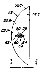
Referring now to the drawings, and particularly to
FIGURE 1, there is illustrated a prior art directional
light system 50. The light system includes a reflector
52 and a light source S~ extending within and in
coaxial alignment with the reflector. The reflector 52
has a substantially truncated parabolic shape. More
particularly, the reflector includes a primary
reflecting surface comprising a base portion 52A, a
lS midsection 52B, a rim portion 52C, and first and second
non-reflective surfaces 52D and 52~. As will be
understood, the surfaces 52D and 52~ may be coated or
formed from a reflective material but do not actively
contribute to the directional light system.
The light source 5~ has a double ended envelope of
quartz material. The light source further has a
central elliptical or bulbous portion 58 and a linear
light-generating filament 60 therein. The envelope has
sealed first and second end portions 62, 6~ extending
coaxially with one another in opposite directions from
the bulbous portion. The linear filament 60 is
positioned in the bulbous portion of the quartz
envelope and supported at opposite ends by the sealed
end portions of the envelope. The light source 5~ is
supported by a pair of upper and lower connector
members 76, 78 extending from a potted plug 80 mounted
in an opening in the rear end of the reflector 52 by a
L 10295
-- 2137585
pair of upper and lower conductor members 82, 84. The
conductor members interconnect the connector members
76, 78 with opposite ends of the filament 60.
Referring to FIGURES 2 - 5, the present invention
is an optical interference filter in the form of a
visible light reflective coating 90 applied on a first
portion of exterior surface 92 of the transparent
envelope. The visible light reflective coating 90 is
applied in a clamshell-shaped pattern. The clamshell
shape is similar to the dumb-bell shape of the
corresponding mating sections that make up the outer
covering on a baseball or tennis ball. More
particularly, the clamshell-shaped coating 90 is a
pattern on the exterior surface of the transparent
envelope that excludes the surface area of the envelope
that is defined by the intersection of all light rays
that pass between the active light generating portion
of the linear filament 60 and the primary reflective
surface 52A, 52B, 52C of the truncated parabolic
reflector. The shape of the clamshell pattern is such
that the primary reflective surface of the reflector 52
would view the light generating portion of filament 60
and the non-reflective surfaces 52D and 52~ would
primarily see the coated surface 90.
2S As best seen in FIGURES 4 and 5, the clamshell
pattern coating 90 covers the top-upper, bottom-lower
and front-face surface portions of the bulbous portion
58 of the envelope whereas the remaining surface of the
envelope defined by the two opposite-side portions and
the rear-face portion is uncoated. The clamshell
pattern of the coating reflects the heretofore unusable
forward-going visible light as well as the heretofore
unusable visible light which diverges in opposite
directions away from the forward-going light and
L 1 0295
2137585
redirects such light toward the filament 60. Much of
this redirected visible light is then scattered off the
filament and into the reflector 52. The coating 90
acts as a light shield to eliminate direct forward
light glare. Also, it should be understood that the
above-described coating pattern is such that the
remaining uncoated portion of the exterior surface of
the transparent envelope permits the active light
generating portion of the filament to be seen at any
point on the primary reflective surface of the
reflector 52.
Due to the axial alignment maintained between the
reflector and the light source, and also due to the
substantial mating of the truncated parabolic shape of
the primary reflective portion of the reflector with
that of the clamshell pattern of the visible light
reflective coating 90 on the envelope of the light
source 5~, the improved directional light system is
capable of producing a light beam pattern having
improved light collection efficiency and enhanced
candlepower while retaining its reduced size. In a
representative example, a tantala/silica multilayer
visible reflecting coating resulted in a 25% increase
in beam lumens relative to uncoated envelopes.
Referring to FIGURES 6 and 7, there is illustrated
a modified embodiment incorporating another
configuration of an optical interference filter in the
form of a combined visib}e and IR light reflective
optical interference coating 110 applied on the first
portion of the exterior surface of the transparent
envelope in a clamshell-shaped pattern. The second
portion or remainder of the exterior surface of the
transparent envelope contains only an IR light
reflective coating 112. In this manner, the entire
L 10295
21 3758~
14
exterior surface of the bulbous portion of the
transparent envelope is reflective to IR light.
Referring now to FIGURES 8 - 10, a related
directional lighting system 150 incorporating features
of the subject invention will be described. In similar
fashion, like elements will be referenced by like
numerals increased by one hundred (e.g., light system
50 a shown in FIGURE 1 will be referenced as light
system 150 in FIGURES 8 - 10) and new elements will be
~0 identified by new numerals. The light system 150
includes an asymmetrical reflector 152 having a
longitudinal axis L, and a linear light source 15~
mounted within the reflector. The light source has a
longitudinal axis 8 extending in coaxial alignment with
the longitudinal axis of the reflector 152. A cover
lens 156 is secured to the front of the reflector. The
reflector has a truncated semi-parabolic shape, an
asymmetrical primary reflective portion 152A and a
focal point that lies on the axis $.
Preferably, the light source 15~ is a double-ended
envelope of quartz material that has a bulbous central
portion 158 and sealed opposite linear end portions
162, 16~. The linear filament 160 is supported at its
opposite ends by the sealed opposite end portions of
the envelope. The light source 15~ is supported above
a base 152E of the reflector by a-pair of inner and
outer connector members 176, 178. The connector
members extend upwardly from the base 152E and are
connected with the opposite ends of the filamen~ 160.
With continued reference to FIGURES 8 - 10, and
additional reference to FIGURES 11 and 12, this light
system uses an optical interference filter in the form
of a light reflective coating 190 applied on a first
portion of the exterior surface of the transparent
213758S L 10295
envelope. The light reflective coating 190 is applied
in a pattern relative to the longitudinal axis of the
light source 8. More particularly, the pattern of the
coating covers the opposite end portions 162, 16~ and
approximately one-half of the bulbous portion 158 of
the envelope. Only an upper aperture or window-like
region 216 of the bulbous portion of the envelope
remains transparent to light. Light emitted upwardly
from the filament through the aperture 216 is reflected
and directed by the asymmetrical reflector 152 either
straight ahead or inclined downwardly, as seen in
FIGURE 8, such as toward a road. There is no light
directed upwardly above the horizontal plane which
extends parallel to the longitudinal parabolic axis L.
In prior art symmetrical reflectors such light causes
glare to oncoming drivers.
The pattern of the coating 190 reflects back
through or past the filament and toward the reflector
light which would otherwise be lost and not used in the
absence of the coating. This improves control and
enhances efficiency of the light beam pattern. Also,
it should be understood that the above-described
coating pattern is such that the remaining uncoated
aperture or window-like region 216 permits the active
light generating portion of the filament 160 to be seen
at any point on the asymmetrical reflective portion
152A of the reflector. The active light generating
portion of the filament 160 extends coaxially,with the
remainder of the filament and the opposite ends 162,
16~ of the envelope with respect to the axis 8.
Referring to FIGURE 12, there is illustrated
another embodiment of the light source 154. The only
difference between the light source in FIGURES 10 and
11 and the light source in FIGURE 12 is that the active
`-- 213758~ . 10295
16
light generating portion of the filament 160 is axially
offset parallel to the remainder of the filament and
the opposite ends of the envelope with respect to the
axis 8 of the light source. By axially offsetting the
filament, much of the light that would normally be
intercepted by the filament and was scattered or
absorbed, is able to reach the active reflector without
a significant increase in apparent source size. This
increases the lumen output without significant loss of
control.
Due to the axial alignment maintained between the
reflector 152 and the light source 15~, and also due to
the substantial matching of the reflective portion 152A
of the semi-parabolic shaped reflector with the pattern
of the visible light reflective coating 190, the
improved direction light system 150 is capable of
producing a light beam pattern having better light
collection efficiency and enhanced candlepower even
though its reduced size is retained. The light beam
pattern is particularly advantageous for use as a low
profile headlamp low beam pattern. In a representative
example, a tantala/silica multilayer visible reflecting
coating was deposited over a portion of an envelope via
LPCVD (Low Pressure Chemical Vapor Deposition). With
the asymmetrical reflector and visible light reflective
coating on the envelope, a 70% increase in useful beam
candlepower can be realized relative to comparable
symmetric reflector design and without the visible
reflective coating on the envelope.
Referring to FIGURE 13, a prior art directional
light system generally designated 250 is illustrated.
For purposes of convenience and consistency, like
elements in the prior art arrangement of FIGURE 13, and
like elements in the embodiments of FIGURES 14 - 20
X13758~ L 10295
employing details of the subject invention, will be
referenced by like numerals increased by two hundred
(e.g., light system 50 as shown in FIGURE l will be
referenced as light system 250 in this embodiment).
Basically, the prior art system 250 includes a
reflector 252 and a light source 254 extending within
and in substantially coaxial alignment with the
reflector 252. A convex lens 256 is secured to the
front periphery of the reflector 252. The reflector in
FIGURE 13 has a substantially truncated parabolic shape
and a longitudinal axis L. The light source 25~ has a
longitudinal axis 8 and is preferably a double-ended
envelope of vitreous material such as quartz. A
central portion of the light source has a substantially
elliptical shape 258 and a linear light-generating
filament 260 disposed inside of the envelope and
extending along the longitudinal axis 8 of the light
source. The envelope also has a pair of sealed
opposite inner and outer linear end portions 262, 26~
(as viewed in FIGURE 13) extending coaxially with one
another along the axis 8 in opposite directions from
the central portion 258. The linear filament 260 is
positioned through the central portion of the quartz
envelope and supported at its opposite ends 260A, 260B
(as viewed in FIGURE 13) by the sealed opposite end
portions 262, 264 of the envelope. The light source
254 is supported with its longitudinal axis 8 in
substantially coaxial relationship with the
longitudinal axis ~ of the reflector 252 by a pair of
upper and lower conductive mounting members 27C, 278
secured to and extending from a potted plug 280
disposed in an opening in the end of the reflector.
Referring to FIGURES 14 and 15, there is
illustrated one embodiment of the light source 25~
~137~85 . 10295
18
improved in accordance with the principles of the
present invention. Specifically, the light source
incorporates one configuration of an optical
interference filter in the form of a visible light
reflective coating 290 partially covering an exterior
surface 292 of the envelope. In this preferred
arrangement, the reflective coating 290 is applied over
approximately one-half of the exterior surface of the
elliptical or bulbous portion 258 and the rearward or
inner end portion 264 in a symmetrical pattern relative
to the longitudinal axis 8 of the light source. The
symmetrical pattern of the coating 290 is such that the
coating shields a first or rearward axial part 294
(FIGURE 15) of the active portion of the light
generating filament 260 and leaves unshielded a second
or forward axial part 29C thereof. The presence of the
coating 290 in the above-described pattern allows the
active length of the filament to emulate a filament of
shorter length than it actually is, thereby yielding a
light beam pattern smaller in angular distribution
relative to the longitudinal axis 8 and larger in
candlepower than would be the case in the absence of
the coating 290.
The coating 290, by shielding the rearward axial
part 294 of the filament active portion, blocks
projection of light from base portions 252A of the
reflector 252 and redirects the light to more desirable
portions thereof. This can be understood by comparing
the sizes of the projected filament images X and Y of
FIGURE 13 with projected filament images A and B of
FIGURE 14. This demonstrates that: (1) high
magnification images X from the base portion 252A of
the reflector, as seen in FIGURE 13, are eliminated by
the reflective coating 292 covering the rearward axial
L 10295
- 2137~85
19
part 29~ of the filament active portion in FIGURE 14;
(2) images A from the midsection 252B of the reflector
in FIGURE 14 have intermediate magnification but view
only forward active part 296 of the filament active
portion, thus producing shorter images than normal and
images that are unusual in that one end originates at
the middle of the filament active portion while the
other end originates at the forward end of the forward
axial part 296 as seen in FIGURE 14; and (3) low
magnification images from near the rim 252C of the
reflector, namely images Y in FIGURE`13 and B in FIGURE
14 are unchanged except for increased intensity of
image B caused by reflections from the coated half of
the filament envelope, for example, the images B at 40
(see FIGURE 18) are increased in intensity by about
50%.
Thus, the combination of the parabolic shape of
the reflector 252 with the symmetrical pattern of the
reflective coating 290 covering a rearward one-half of
the exterior surface 292 of the envelope of the light
source 25~ improves the angular distribution pattern by
providing a sharp beam cutoff, thereby enhancing the
candlepower of the light beam produced by the light
system 250. In a representative example, a
tantala/silica multilayer visible reflecting coating
was deposited over a portion of an envelope via LPCVD
(Low Pressure Chemical Vapor Deposition) using borate
masking for the coating pattern. -This process will be
described in greater detail below. A reduction in beam
diameter of about 50% with increased uniformity of the
central light spot and an increased brightness relative
to uncoated envelopes was provided by the coating.
FIGURE 18 is a graph plotting the intensity or
candlepower of the light beam produced by coated and
L 10295
- ~13758~
uncoated envelopes versus the angle of the beam
relative to the longitudinal axis of the reflector.
The chart in FIGURE 19 shows the candlepower
distribution around the light source 254 of FIGURE 13
having the uncoated transparent envelope. In contrast,
the chart of FIGURE 20 shows the candlepower
distribution around the light source of FIGURES 14 and
15 having the visible light reflective coating 290 over
one-half of the transparent envelope. The improved
distribution and increased candlepower of the light
beam in FIGURE 20 is readily apparent over that of
FIGURE 19.
Referring to FIGURE 16, there is illustrated a
modified embodiment of the light source 25~
incorporating another configuration of an optical
interference filter in the form of a visible light
reflective coating 290. The coating has a primary
portion 300 substantially in the same pattern as the
coating described above with reference to FIGURES 14
and 15. Also, the reflective coating in FIGURE 16 has
a secondary portion 302 spaced from the primary portion
300 and applied on the exterior surface of a section of
the forward or outer end 262 of the envelope where it
attaches to the bulbous portion 258.
Referring to FIGURE 17, there is illustrated
another modified embodiment of the light source 254
incorporating the same coating pattern as in FIGURES 14
and 15. However, whereas the active portion of the
filament 260 in FIGURES 14 and 15 extends coaxial with
the longitudinal axis 5 of the- light source 25~, in
FIGURE 17 the active portion of the filament extends in
an axially offset relation to the longitudinal axis 8.
In all of the above-described embodiments, the
light source is substantially coaxial or parallel to
213~58~ L 10295
the axis of the reflector. As shown in FIGURES 2l -
27, the light system 350 positions the reflector axis
L generally perpendicular to the light source axis S.
Like elements are referenced by like numerals increased
by three hundred (e.g., reflector 52 will be referenced
as reflector 352) and new elements will be identified
by new numerals. More particularly, and as illustrated
in FIGURE 2l, the prior art system includes a reflector
352 and a light source 35~ extending within the
reflector. The reflector has a substantially parabolic
shape and a longitudinal axis ~. The light source 354
has a double-ended envelope substantially similar to
the light sources described in the prior embodiments.
The light source 354 is supported between a pair of
upper and lower conductor members 376, 378 extending
from a potted plug 380 mounted in an opening in the
rear end of the reflector 352. The light source is
supported by the conductor members so as to extend in
a transverse, preferably substantially perpendicular,
relationship to the longitudinal axis ~ of the
reflector 352.
Referring to FIGURES 22 and 24, there is
illustrated another embodiment of the light source 354
improved in accordance with the principles of the
present invention by incorporation of one configuration
of an optical interference filter in the form of a
visible light interiorly-reflective coating 390.
Preferably, the coating is applied on a first portion
of an exterior surface of the transparent envelope of
the light source. The visible li-ght reflective coating
390 is approximately semi-cylindrical in profile and
occupies approximately one-half the exterior surface
area of the envelope. More particularly, the coating
390 is applied on the envelope exterior surface that
L 10295
- ~137~85
faces away from the reflector 352. The first portion
of the envelope exterior surface covers approximately
one-half of the entire surface and lies along one of a
pair of opposite sides of a plane defined along and
through the longitudinal axis 8 of the light source.
Therefore, the coating pattern is applied to the
envelope in an asymmetrical relation to the
longitudinal axis 8.
It should be understood that in FIGURES 22 - 25,
the coating 390 is shown as occupying approximately
one-half of the exterior surface, however, this
relationship is for the specific case wherein the
filament 360 and the focal point of the parabolic
reflector 352 lie at the edge of the reflector. For
lS use with deeper reflectors, those having a greater
curvature whereby its focal point is beyond the edge of
the reflector, it has been found that the optimum
coating pattern is less than one-half of the exterior
surface, or approximately one-third of the exterior
surface. Also, it should be understood that the above-
described coating pattern is such that the remaining
uncoated portion of the envelope exterior surface
permits the active light generating portion of the
filament to be seen at any point on the reflector.
The pattern of the coating 390 reflects the
visible light emitted by the filament 360 away from the
reflector 352 and redirects such light toward the
active portion of the reflector. The coating acts as
a light shield to eliminate direct forward light glare.
The active light generating portion of the filament
extends coaxially with the remainder of the filament
360 and the opposite ends 362, 36~ of the envelope with
respect to the axis 8.
Referring to FIGURES 23 and 25, there is
213758~ . 10295
illustrated another embodiment of the light source 35~.
The only difference between the light source in FIGURES
23 and 25 and the light source in FIGURES 22 and 24 is
that the active light generating portion of the
filament 360 is axially offset but parallel to the
remainder of the filament. In other words, the active
light generating portion of the filament is offset and
parallel to the opposite ends 362, 36~ of the envelope
with respect to the axis 8.
lODue to the transverse alignment maintained between
the reflector 352 and the-light source 354, and also
due to the substantial mating of the shape of the
reflective portion 352A of the reflector 352 with that
of the pattern of the visible light reflective coating
15390 on the envelope of the light source 35~, the
improved directional light system is capable of
producing a light beam pattern having improved light
collection efficiency and enhanced candlepower even
though its miniature size is retained. Further
enhancement of beam lumens is realized by offsetting
the active light-generating portion of the filament 360
from the longitudinal axis 8 of the light source 35~.
In a representative example, a tantala/silica
multilayer visible reflecting coating was deposited
over one-half of the envelope via LPCVD (Low Pressure
Chemical Vapor Deposition) and resulted in a 50%
increase in beam lumens with 50% higher maximum
candlepower relative to uncoated envelopes.
The chart in FIGURE 26 shows the candlepower
distribution around the light source of prior art
devices having an uncoated envelope as in FIGURE 2l.
In contrast, the chart of FIGURE 27 shows the
candlepower distribution around the light source 35~ of
FIGURE 22 having the visible light reflective coating
213758~ 10295
390 over one-half of the transparent envelope. The
improved control and increased candlepower of the light
beam in FIGURE 27 is readily apparent over that of
FIGURE 26.
Two related embodiments are illustrated in FIGURES
28 - 35. The similarities with previously described
embodiments is apparent, e.g., FIGURES 2 - 7. These
further embodiments demonstrate the applicability of
features of this invention to light sources other than
incandescent type light sources. As shown in FIGURES
28 - 3l, an arc discharge lamp is shown in a truncated
parabolic reflector. More particularly, FIGURE 28
shows an arc discharge lamp 454 situated within a
reflector 452. The lamp is held in place by metal
connectors 476, 478 that depend, respectively, from
conductors 482, 484 mounted on a potted end 480. The
reflector comprises a substantially parabolic, primary
reflecting surface 452A, and-upper and lower planar
surfaces 452D and 452E, respectively. Planar surfaces
452D and 452~ limit, or truncate, the vertical extent
of parabolic reflecting surface and are thus also
referred to as planar "truncating" reflecting surfaces.
As discussed above, the planar truncating surfaces play
a far less active role than the primary reflecting
surface 452A in reflecting light forwardly from the
lamp.
The arc discharge light source is preferably of
the metal halide type. It includes a refractory light-
trans~issive envelope comprising longitudinal ends 462
and 464, and an intermediate bulbous region 458
containing a sealed chamber. Electrodes 518 and 520
are spaced apart from each other by an arc gap 521 in
the chamber which also inclùdes a gaseous fill that
typically includes a metal halide. The electrodes are
~13 758~ L 10295
approximately aligned with the longitudinal axis L of
the light source, at least in the vicinity of bulbous
region 458. Preferably, such longitudinal axis L, in
turn, is substantially aligned with a longitudinal axis
(not shown) of the parabolic reflecting surface 452.
Tn conventional manner, electrode 518 is connected by
a lead 522 and refractory foil 524 to an inlead 526.
Similarly, electrode 520 is connected by a lead 532 and
refractory metal foil 534 to an inlead 536. Although
not shown, leads 522, 532 are typically wrapped, in
conventional manner, with respective coils of wire to
facilitate alignment of such leads along longitudinal
axis L.
In the example shown, an outer arc tube envelope
540 of light-transmissive refractory material is formed
over the light-transmissive envelope and comprises ends
542, 5~ spaced from each other along longitudinal axis
L, and an intermediate bulbous-region 546. The ends of
the outer envelope are respectively attached to ends
462, 464 of the envelope by melting and fusing together
the adjacent envelope and outer envelope ends. If
desired, space ~60 between the envelope and the outer
envelope can be placed under vacuum, as taught, for
instance, in U.S. Patent 4,935,668 issued to Richard L.
Hansler, et a}. and assigned to the instant assignee.
Further, the-outer-envelope can be~mounted in relation
to the envelope with other geometri-es (not shown), such
as by fusing the outer envelope ends 54Z, 544 directly
to the inleads 526, 536, respectively. The foregoing
method of attachment is also taught in the foregoing
'668 patent.
Substantially all of the outer envelope bulbous
region to the right of plane P is coated with a visible
light-reflecting coating 490. ~oating 490 reflects
L 10295
2 1 3 7 ~ 8 j
26
light emitted by the arc discharge back towards the arc
discharge. For this purpose, outer envelope bulbous
region 546 has a substantially elliptical or spherical
shape along longitudinal axis L. As a result, the
light directed to parabolic reflecting surface 452A of
the light source can be effectively controlled by the
reflecting surface to achieve a desired beam pattern.
Visible-light reflecting coating 490 is positioned
on light source ~54 as shown in FIGURE 28, and also in
the simplified top and side plan views of lamp shown in
FIGURES 30 and 31, respectively. In FIGURE 30, light
rays comprise two components. The primary reflecting
surface 452A receives a first component in a non-
reflected condition, and a second component that has
been reflected from coating 490 and redirected towards
the arc discharge in arc gap 521. Because the
discharge is largely transparent to its own radiated
light, the second component of light largely passes
through the discharge to reach the primary reflecting
surface. The primary reflecting surface 452A then
directs the cumulative first and second components of
light forwardly as light rays. The side plan view of
FIGURE 31 similarly shows light rays following the
mentioned pattern of light rays of FIGURE 30, and being
reflected by reflecting surface 452A in a forward
direction.
If the parabolic reflecting surface collects, for
instance, about one third of the light reflected by
coating 490, with an apparent position coincidir,g with
the arc discharge, the beam lumens can be theoretically
increased by about 20% to 30%. Visible light-
reflecting coating 490 may, for instance, comprise
twenty-seven alternating layers of tantala and silica
deposited on the envelope by LPCVD (Low Pressure
~13758S L 10295
Chemical Vapor Deposition), using borate masking to
achieve the pattern shown and to be described in
greater detail below.
The foregoing coating is refractory, and thus able
S to withstand the high temperatures encountered during
operation of the light source. In contrast, a
conventional metal coating (e.g., aluminum or silver)
would fail under such operating temperatures. The
described coating, moreover, forms an optical
interference filter, which is specular, or mirror-like,
and which considerably aids in reflecting light rays
towards longitudinal axis L of the light source. On
the other hand, diffuse coatings that reflect visible
light, formed of powdered material such as alumina, are
far less capable of reflecting light towards
longitudinal axis L. Accordingly, diffuse coatings
increase the apparent size of the light source as
"seen" by the parabolic reflecting surface, resulting
in a less-controlled beam, typically with glare. The
foregoing, distinguishing features of the described
coating ~90 preferably apply to all other visible
light-reflecting coatings referred to herein.
Another desirable property of an optical
interference filter is that it can be designed to
selectively transmit, or to reflect, light in different
frequency ranges. Thus, when formed of an optical
interference filter, coating ~90 can be designed to
reflect infrared light, or to transmit an undesirable
color of visible light, for instance. T~is is
accomplished by selecting layer thicknesses and layer
count for a given set of high and low index of
refraction materials.
Yet another advantage offered by the optical
interference filter is improved color mixing. With
-- 213 7~8a L 10295
conventional arc lamps, color separation can occur.
The addition of the reflective coating directing
portions of the emitted radiation through the
essentially transparent source provides color mixing.
In addition to increasing beam lumens, visible
light-reflecting coating 490 on the light source of the
foregoing FIGURES 28 - 3l also serves as a light shield
to prevent direct forward-going light from the light
source from being projected forwardly. Such direct
forward-going light lacks the high degree of
directional control gained from being reflected by
parabolic reflecting surface 452A. In an automobile
headlamp, for instance, an oncoming driver observing
the headlamp is protected from the glare caused by such
uncontrolled light.
FIGURES 32 - 35 show another light source of the
arc discharge type. With the exception of the
configuration of visible light-reflecting coating 490
on the light source of FIGURE 32, the other parts of
such light source conform to the above description of
the like-numbered parts.
Visible light-reflecting coating 490 on the light
source defines a clamshell pattern (FIGURES 32 and 33)
in a manner similar to the embodiments of FIGURES 2 -
7. The clamshell pattern is preferably configured such
that an arc in the arc gap can be "seen" from any point
on the primary reflecting surface 452A, but, to the
extent possible, not from any point on planar
truncating surfaces 452D and 452E. Owing to the
preferably spherical or elliptical shape of that
portion of outer envelope bulbous region covered with
coating 490, light from an arc in the arc gap received
by, and reflecting from, the coating is focussed back
through the arc. As a result, the light directed to
L 10295
-- 213758~
parabolic reflecting surface ~52A can be most
effectively controlled by such parabolic reflecting
surface to achieve a desired beam pattern.
FIGURES 34 and 35 respectively show simplified top
and side plan views of the light system having the
described clamshell pattern. The illustrated light
rays show that the upper and lower sides of the
clamshell pattern (see FIGURE 32) substantially prevent
light rays from the light source from reaching planar
truncating reflecting surfaces ~52D and 452F. Light
rays reaching these surfaces are nearly useless, since
such surfaces fail to reflect light in the forward
direction. The clamshell pattern of coating instead
receives light that would otherwise uselessly reach
planar truncating surfaces and redirects it, as shown
by the light rays, rearwardly to the parabolic, primary
reflecting surface. The primary reflecting surface
then reflects the light in a useful forward direction.
Of course, the illustrated light rays also have a
component of light that is received by reflecting
surface directly from the arc discharge.
Additionally, the clamshell pattern of visible
light-reflecting coating ~90 of light source blocks
non-reflected light from the arc discharge from being
directly sent in a forward direction. Such direct
forward-going light, avoided by the clamshell pattern,
would add a component to the forward light beam that
lacks the high degree of directional control gained
from being reflected by parabolic reflecting surface.
An increase in beam lumens in excess of 20% is
expected for the clamshell coating pattern compared
with uncoated light sources. For such purposes,
visible light-reflecting coating ~90 may be formed by
depositing alternating layers of tantala and silica on
.
L 1 0295
-- ~13758~
the envelope by LPCVD, using borate masking to achieve
the pattern shown.
FIGURE 36 represents yet another type of lighting
system or lamp to which the principles of the subject
invention apply. As shown, an electrodeless high
intensity discharge lamp 600 has an arc tube 602 that
contains ia fill of ionizable gas 60~. A high frequency
RF signal is supplied by an excitation coil 606 to
excite the ionizable gas to a gas discharge state. A
starting aid 608 is associated with the arc tube and
usually constructed from a similar fused quartz
material. A low pressure gas or gas mixture 610 has a
lower dielectric breakdown value than the gas fill 604
so that it achieves a state of electric discharge
initiated by starting circuit 612. Once the gas 610
has reached a state of electric discharge, it serves-to
initiate the electric discharge within the arc tube
602. In this manner, visible radiation is emitted from
the lamp. Particular details of this type of
electrodeless lamp are well known in the art so that
further discussion herein is unnecessary.
In accordance with the subject invention, portions
of the arc tube 602 and/or the starting aid 608 can be
provided with an optical interference filter or coating
620. Selected portions of the emitted radiation are
reflected back toward the arc discharge, at least a
portion of which is converted to visible light
radiation and an overall increase in efficiency.
Moreover, coating selected portions of the light source
permits a designer to pr~ject the light in
predetermined orientations and patterns.
In order to obtain such patterned interference
filters, the envelope is first masked with a solid
masking material which is able to undergo viscous flow
213 75~ L 10295
under stress at a temperature broadly ranging between
250-700C and which is soluble in a medium which will
not adversely affect either the filter material or the
envelope. The mask is applied to the envelope in a
pattern which, when removed from the envelope after
deposition of the filter, leaves the filter on the
substrate in the desired pattern. The multilayer
optical interference filter is applied to the masked
envelope by any suitable means known to those skilled
in the art.
In one embodiment of the invention, a precursor of
a masking material, such as a boric oxide precursor, is
applied to an external surface of the light source
envelope. The precursor is then converted to boric
oxide prior to deposition of the-multilayer filter or
coating. In another embodiment, the boric oxide
material or a precursor thereof is applied to the
envelope via a chemical vapor deposition process. With
a vapor deposition, evaporation or sputtering masking
process, the envelope must first be premasked or coated
with a suitable material, such as decals, tape, organic
coating compounds such as lacquers, etc., and the boric
oxide precursor applied over the premasked envelope.
The decal, tape or lacquer premask is applied to the
envelope in the pattern in which the patterned
interference filter is desired and the boric oxide or
boric oxide precursor applied over the premasked
envelope.
Alternatively, the premask may be achieved by use
of a mechanical mask or stencil-combined with spraying
the boric oxide precursor onto the envelope. A
mechanical premask will also work well with line-of-
sight processes, such as evaporation, sputtering or
other physical vapor deposition (PVD) methods for
213 7~&5 . 10295
applying the boric oxide or precursor thereof. Boric
oxide, or a boric oxide precursor, can also be applied
by spraying, dipping or daubing an aqueous slurry of
either of these materials in a saturated solution of
same with the viscosity adjusted by using a suitable
viscosifier such as methyl cellulose or acrylic acid
which can later be burned out leaving the boric acid.
After deposition for formation of the boric oxide
or boric oxide precursor, the premask is dissolved off
the envelope in a liquid or vapor media which does not
dissolve or adversely affect either the boric oxide,
boric oxide precursor or envelope. Alternatively, some
premasking compounds, such as a lacquer, may be removed
in-situ via pyrolysis during conversion of the boric
lS oxide precursor to the boric oxide. In some
embodiments, a premask is not needed and the envelope
is either partially immersed in a liquid boric oxide
precursor or the precursor is brushed, painted or
daubed onto the envelope such that the desired pattern
for the optical interference filter (which will be
applied over the masked envelope) is achieved after
removal of the boric oxide.
Tributyl borate and trimethoxyboroxine are liquid
boric oxide precursors that have been found to be
useful in the practice of the invention and have been
applied to substrates such as envelopes by dip coating,
painting, brushing and daubing. By way of example, a
lamp, such as an incandescent lamp having a fused
quartz or glass lamp envelope, is dipped in, brushed,
painted or daubed with the viscous, liquid tributyl
borate or trimethoxyboroxine only on those portions of
the envelope surface where the optical interference
filter is not desired. Excess tributyl borate liquid
on the lamp envelope is removed by using a fibrous
L 10295
~137~8S
33
material such as a capillary wicking device. The lamp
envelope to which the tributyl borate (or
trimethoxyboroxine) has been applied is then contacted
with water, steam or a high humidity environment (such
as by placing the coated lamp envelope over boiling
water) to convert the precursor liquid to boric acid.
The tributyl borate or trimethoxyboroxine reacts with
H20 to form boric acid (H3B03). This produces a frosty
appearing, solid boric acid on the envelope where the
liquid tributyl borate precursor was present.
The so-formed boric acid is somewhat porous, has
pinholes and is easily damaged or marred by handling.
Consequently, it must be densified and converted to
boric oxide (B203) to be useful in the practice of the
invention. This is readily accomplished by heating to
a suitable elevated temperature typically in the range
of from 550C-800C to convert the boric acid to boric
oxide. The elevated temperature also removes any
residual organic material present and promotes good
adhesion between th-e boric oxide coating and the
vitreous substrate. Heating in air for five to ten
minutes at 650C has worked well in-the laboratory.
The boric oxide is a glassy material which
exhibits viscous flow at temperatures of 250C and
higher (i.e., 250-700C) which-is a beneficial and
important feature in the practice of the process of-the
invention. The viscous flow eliminates defects, such
as pinholes, in the mask.- It also serves to relieve
the intrinsic stress that occurs during --vapor
deposition processes when applying the filter over the
masked envelope. If this stress is not relieved, the
mask may spall during formation of the filter which
means that the filter will also be applied to the
envelope where spalling has occurred. This, of course,
3758~ L 10295
34
is undesirable.
This intrinsic stress is that which is inherent
from the deposition process and is not the same as that
which would occur from differential thermal expansion
and contraction. When applying optical interference
filters made of refractory metal oxides, the slight
viscous flow of the boric oxide mask results in
cracking of the overlying interference filter material
which aids in the subsequent removal of the mask and
overlying filter. The non-crystalline, glassy nature
of the boric oxide also adds to less film defects in
the mask, because no tensile stresses are produced in
the mask due to morphological phase changes which would
occur with a crystalline material. Therefore, in order
to be useful as a mask with optical interference filter
deposition processes which occur at elevated
temperatures, such as chemical vapor deposition
processes (CVD), the masking material should preferably
exhibit viscous flow in order to relieve stress and
avoid spalling and cracking of the mask during the
filter deposition process.
In general, the boric oxide mask may broadly range
between about O.l to 2 microns in thickness, with 0.5
to 0.7 microns being preferred. Too thick a coating
can cause failure in a glass or fused quartz envelope
due to the thermal expAncion mismatch between the boric
oxide in its solid state and the silica envelope. If
it is too thin, pinholes may resu-lt and the mask may~be
more difficult to remove.
In order to achieve a boric oxide mask thickness
on the order of one micron or more, more than one
application of the tributyl~borate-precursor followed
by hydrolysis to boric acid-may be necessary.- Using
trimethoxyboroxine has resulted in a one micron thick
,
~ 13 7 ~ 10295
mask using only one dip. In the case of dip coating,
an outer envelope surface of a lamp, or the filament or
arc chamber of a light source is dipped into liquid
tributyl borate at room temperature. With tributyl
borate, it was found that one dip resulted in a
densified boric oxide film only one-half micron thick
after hydrolysis and conversion to the oxide.
Repeating the process produced a boric oxide thickness
around one micron.
The boric oxide mask precursor, i.e., boric acid,
has also been produced by an Atmospheric Pressure
Chemical Vapor Deposition (APCVD) process by reacting
trimethyl borate vapor with water vapor at room
temperature in a reaction chamber containing the object
or envelope to be masked. In this process, a stream of
nitrogen gas is bubbled through liquid trimethyl borate
and another stream of nitrogen gas-is bubbled through
water vapor with the two streams separately fed into a
reaction chamber containing the lamp or other object to
be masked. The trimethyl borate vapor reacts with the
water vapor which forms a boric acid (H3B03) coating on
the envelope which is then heated to form the boric
oxide. A one (l) micron thick coating of boric oxide
is readily achievable using this process. As with the
liquid metallo organic precursor process, the so-formed
boric acid must be heat treated to densify it and to
convert it to boric oxide and a temperature of about
650C for five to ten minutes as disclosed above has
been found to be suitable.
In the APCVD process, complex symmetric and
asymmetric boric oxide mask patterns have been achieved
by using various premask materials such as decals and
adhesive tape. After the boric acid has been formed,
the decal or tape is removed an~ the boric acid
- ~13758S 10295
remaining on the coated envelope is converted to boric
oxide by heating.
After the boric oxide coating has been formed, the
desired multilayer optical interference filter is
applied to the boric oxide masked envelope. This may
be done using any well known deposition process
presently employed for applying such filters including,
for example, vacuum evaporation, ion plating,
sputtering, Chemical Vapor Deposition (CVD) processes
such as plasma CVD, Atmospheric Pressure CVD (APCVD)
and Lower Pressure CVD (LPCVD).
In practicing the process of this invention,
refractory metal oxide multilayer optical interference
filters made of alternating layers of titania and
silica and also of tantala and silica for a total of
from twenty-six to thirty-two layers have been applied
to the outer surface of the filament and arc chambers
of electric lamps at a temperature within the range of
350-600OC using an LPCVD process. This portion of the
process is disclosed in U.S. Patent Nos. 4,949,005 and
5,138,219 assigned to the assignee of the present
invention, the disclosures of which are incorporated
herein by reference. The '005 patent also discloses
annealing filters of tantala and silica at a
temperature between 550-675C.
In summary, prior to applying the optical
interference filter, those portions of the outer
surface of the lamp envelope shown as not coated are
premasked with a decal. The premasked lamp is then
dipped in tributyl borate, withdrawn, and excess
tributyl borate removed by wicking with a paper towel.
The tributyl borate-coated lamp is held over boiling
water to hydrolyze the borate to boric acid and then
placed in a 650C oven for ten minutes to convert the
L 10295
213758~
boric acid to boric oxide. This process may be
repeated a second time.
The cold mirror described above is then applied
over the boric oxide masked lamp using an LPCVD process
at a temperature in the range of 350-600C. After the
filter is formed over the masked lamp, the lamp is
cooled and placed in water which dissolves the boric
oxide, removing it and the filter material applied over
it. The lamp is then heat-treated to anneal the
remaining cold mirror patterned optical interference
filter following the annealing schedule in the '005
patent.
The invention has been described with reference to
the preferred embodiments and methods of forming same.
Obviously, modifications and alterations will occur to
others upon a reading and understanding of this
specification. It is intended to include all such
modifications and alterations insofar as they come
within the scope of the appended claims or the
equivalents thereof.