Note : Les descriptions sont présentées dans la langue officielle dans laquelle elles ont été soumises.
CA 02138218 2000-OS-10
PROCESS FOR DELAMINATING ORGANIC RESIN
FROM BOARD AND PROCESS FOR MANUFACTURING
ORGAPJIC RESIN MULTI-LAYER WIRING BOARD
The present invention relates to a process for delaminating an organic
resin from a board. In addition, the present invention relates to a process
for
manufacturing an organic resin multi-layer wiring board, and more particularly
to a process for manufacturing an organic resin multi-layer wiring board by
connecting a plurality of blocks.
The process of delaminating organic resins from boards is carried out in
a variety of situation:. during the manufacture of boards for mounting
electronic
devices. For example, in a iprocess for manufacturing a certain organic resin
multi-layer wiring board, the organic resin is delaminated from the board.
According to this manufacturiing process, a plurality of separately
manufactured
blocks with wiring layers are connected to each other. The connected blocks
are incorporated into a multi-layer wiring board. The blocks are organic resin
multi-layer wiring layers. The blocks are laminated on a board. In preparation
for connection, the blocks arE~ delaminated from the boards. An instance of
this
manufacturing process is disclosed in Japanese Patent Koukai Hei No. 5-
206643. The technique described in this publication dissolves the board for
separation of the block and the board. More specifically, an aluminum board is
dissolved in an aqueous solution of hydrochloric acid. This delaminating
technique is, however, troublesome in that the aqueous solution of
hydrochloric
acid deteriorates the organic. resin multi-layer wiring layer.
An object of the present invention is to provide a process for delaminating
an organic resin which does not adversely affect portions other than the
portion
to be delaminated.
A further object of the present invention is to provide a process for
manufacturing an on~anic resin multi-layer wiring board with a high degree of
reliability.
-1-
CA 02138218 1998-09-10
A still further object of the present invention is to provide a process for
manufacturing an organic resin multi-layer wiring board for a shorter term.
The process for delaminating an organic resin according to the present
invention causes a photochemical reaction of the organic resin to weaken the
adhesive force between the organic resin and the board. Since the section of
the organic resin which is in contact with the board is irradiated with light,
it is
necessary to use a board which transmits the light. The light applied to the
board is transmitted through the board and reaches the organic resin.
More precisely, the process for manufacturing an organic resin multi-layer
wiring board by connecting a first block with a second block according to the
present invention comprises the steps of:
(A) forming a first block on a first board, wherein said first board is
capable of transmitting light, and comprising the following steps (a), (b) and
(c):
(a) forming a first organic resin on said board, wherein said first
organic resin layer is capable of undergoing a photochemical reaction by
exposure to light;
(b) alternatingly laminating on said first organic resin layer, a
wiring layer and an organic resin insulation layer; and,
(c) laminating a first organic resin adhesive layer on said
organic resin insulation layer or said wiring layer arranged in Step (b);
(B) forming a second block on a second board, and comprising the
following steps (d) and (e):
(d) alternatingly laminating on a second board, an organic resin
insulation layer and wiring layer; and,
(e) laminating a second organic resin adhesive layer on said
organic resin insulation layer or said wiring layer formed in Step (d);
(C) connecting said first block with said second block and comprising
the following steps (f) and (g):
(f) facing said first organic resin adhesive layer of said first
block to said second organic resin adhesive layer of said second block; and,
-2-
CA 02138218 1998-09-10
(g) heating and pressing said first block and said second block
to adhere said first organic resin adhesive layer to said second organic resin
adhesive layer; and,
(D) delaminating said first block from said first board and comprising
the following steps (h) and (i):
(h) irradiating the side opposite to the side of said first board
which has said first organic resin layer, with said light which is transmitted
through said first board and reaches said first organic resin layer to cause
the
section of said organic resin layer which adheres to said first board to
undergo
a photochemical reaction by exposure to said light, thereby lowering the
adhesive force between said first organic resin layer and said first board;
and,
(i) delaminating said first block from said first board.
In the above manufacturing process, the first board may be removed prior
to the connection between the first block and the second block. For this,
however, the adhesion between the first block and the second block must be
temporary.
Other objects, features and advantages of the present invention will
become more apparent when the following description is read in conjunction
with the accompanying drawings, wherein:
Figure 1 is a schematic view of Example 1 according to the present
invention;
Figures 2 to 7 are sectional views of a first block 100 in Steps 1 to 6,
respectively, of Example 1;
Figures 8 to 13 show sectional views of a second block 200 in Steps 7
to 12, respectively, of Example 1;
Figure 14 is a sectional view of a first block 100 and a second block 200
connected to each other in Step 13 of Example 1;
Figures 15 to 17 illustrate a process for delaminating a quartz glass
board in Steps 14 to 16, respectively, of Example 1;
Figures 18 to 20 are sectional views of a block laminate 1200 in Steps
17 to 19, respectively, of Example 1;
_3_
CA 02138218 1998-09-10
Figure 21 is a sectional view of a third block 300 and a block laminate
1200 connected to each other in Step 20 of Example 1;
Figure 22 is a schematic view of Example 2 according to the present
invention;
Figure 23 is sectional views of a first block 100 and a second block 200
connected to each other in Step 22 of Example 2;
Figure 24(a) through Figure 31(a) and Figures 32-36 are sectional views
of intermediate products in Steps 1 to 13, respectively, of Example 3
according
to the present invention;
Figure 24(b) through Figure 31 (b) are plan views of intermediate products
in Steps 1 to 8, respectively, of Example 3;
Figure 37 is a sectional view of a multi-layer wiring board completed in
Step 14 of Example 3;
Figure 38(a) through Figure 45(a) are sectional views of intermediate
products in Steps 1 to 8, respectively, of Example 4;
Figure 38(b) through Figure 45(b) are plan views of intermediate products
in Steps 1 to 8, respectively, of Example 4;
Figure 46 through Figure 49 are sectional views of intermediate products
in Steps 15 to 18, respectively, of Example 4; and,
Figure 50 is a sectional view of a multi-layer wiring board completed in
Step 19 of Example 4.
In these figures, the same reference numerals depict the same parts,
respectively.
EXAMPLES
Example 1
Example 1 of the present invention will now be described with reference
to the accompanying drawings.
First, an outline of the manufacturing process of Example 1 will be
described. Referring to Figure 1, the manufacturing process of Example 1
includes Steps A-G. Of these steps, Step D is the step characteristic of the
present invention.
-4-
CA 02138218 1998-09-10
With reference to Figures 1-7, in Step A, a block 100 is formed on a
board 111. Step A includes Steps 1-6. Referring to Figure 1 and Figures 8-13,
a block 200 is formed in Step B. Step B includes Steps 7-12. Steps A and B
may be carried out in any order. Steps A and B may be conducted
simultaneously. Referring to Figure 1 and Figure 14, in Step C, the first
block
100 and the second block 200 are connected to each other by heating and
pressing. Step C includes Step 13.
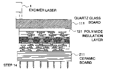
Referring to Figure 1 and Figures 15-17, in Step D, excimer laser
irradiation of the block 100 delaminates the block 100 from the board 111.
This
step is characteristic of the present invention. Step D includes Steps 14-16.
With reference to Figure 1 and Figures 18-20, in Step E, in order to
connect the first block 100 with a third block, a bump 126 and a via hole 1242
are formed on the surface of the first block 100. Step E includes Steps 17-19.
Referring to Figure 1, in Step F, a third block 300 is formed. Step F may
be carried out any time. Step F may be carried out at the same time as Step
AorB.
Referring to Figure 1 and Figure 21, in Step G, a connection is
established between the first block 100 and the third block 300. Step G
includes Step 20.
Next, an explanation will be made of Steps 1-21.
Matters Common to Steps
First, an explanation will be given regarding matters common to all the
steps.
In the organic resin multi-layer wiring board of the present example, a
polyimide is used as the organic resin which composes the insulation layer.
The thickness of the polyimide insulation layer is 20 Vim. The film thickness
of
the wiring layer is 10 ~cm, and the wiring width of the wiring layer is 25
~,m. In
addition, the diameter of a via hole which connects the wiring layers is 100
~,m.
Unless otherwise specified, dimensions of the polyimide insulation layers,
wiring
layers and via holes to be formed in the present example conform to the above-
mentioned.
-5-
CA 02138218 1998-09-10
In this connection, a photosensitive polyimide with a low coefficient of
thermal expansion is used to form the polyimide isolation layer. Here, the
"photosensitive polyimide with a low coefficient of thermal expansion" is
defined
to be a photosensitive polyimide with a coefficient of thermal expansion of
from
10-30 ppm. On the other hand, a polyimide resin having a glass transition
point
is used as the polyimide adhesive layer.
The wiring layer and the bump are formed from gold. More concretely,
they are formed by electrolytic plating of conductor patterns. The conductor
patterns are formed by photolithographic techniques using photoresists.
Step A
Referring to Figure 2 through Figure 7, in Step 1 through Step 6, a first
block 100 is formed on a quartz glass board 111.
Step 1
Referring to Figure 2, in Step 1, a uniform polyimide insulation layer 121
is formed on the quartz glass board 111. The quartz glass board 111 has a
thickness of 2 mm. In addition, the polyimide insulation layer 121 is formed
using a photosensitive polyimide with a low coefficient of thermal expansion.
The thickness of the polyimide insulation layer 121 is 10 ~cm.
Step 2
Referring to Figure 3, in Step 2, a wiring layer 131 is formed on a
polyimide insulation layer 121. This wiring layer 131 is used for connection
wiring, and also for wiring for ground connection.
Stee 3
Referring to Figure 4, in Step 3, a polyimide insulation layer 122 is
formed on the wiring layer 131. In the polyimide insulation layer 122 there is
formed a via hole 141. The polyimide insulation layer 122 and the via hole 141
are formed in the following steps.
In the first step, varnish of a photosensitive polyimide with a low co-
efficient of thermal expansion is applied to a wiring layer 131.
In the second step, the applied polyimide varnish is exposed and
developed to form a via hole 141 therein.
-6-
CA 02138218 1998-09-10
In the third step, the polyimide varnish with the via hole 141 formed
therein is cured. The polyimide insulation layer 122 and the via hole 141 are
formed in this manner.
The polyimide insulation layer 122 has a thickness of 20 ~,m.
Step 4
Referring to Figure 5, in Step 4, a wiring layer 132, a polyirnide insulation
layer 123 and a wiring layer 133 are layered on a polyimide insulation layer
122
in that order. These layers are formed by carrying out the process of Step 2
and Step 3 repeatedly. These layers have the same measurements and quality
of material as those formed in Step 2 and Step 3.
Step 5
Referring to Figure 6, in Step 5, a polyimide adhesive layer 151 and a via
hole 143 are formed on the wiring layer 133. The polyimide adhesive layer 151
and the via hole 143 are formed in the following steps.
In the first step, polyimide varnish having a glass transition point is
applied onto the wiring layer 133. This polyimide varnish forms a polyimide
adhesive layer 151. That is, the polyimide adhesive layer 151 and the
polyimide
insulation layers 121-123 are different in the properties of the polyimides
used.
In the second step, the applied polyimide varnish is subjected to
exposure and development to form a via hole 143 therein.
In the third step, the polyimide varnish is cured. The polyimide adhesive
layer 151 and the via hole 143 are formed in this manner. The polyimide
adhesive layer 151 is 10 ~.m thick.
Step 6
Referring to Figure 7, in Step 6, a bump 161 is formed. The bump 161
connects a first block with a second block as prepared in the steps described
later. The bump 161 is connected to the wiring layer 133 through the via hole
143.
The bump 161 is formed by metal plating. The metal deposit consists of
four skins. The materials of the first through fourth skins are nickel, gold,
tin
and gold, respectively. The first skin is located closest to the metal
patterns.
-7-
CA 02138218 1998-09-10
The first through fourth metal skins are 3 Vim, 8 Vim, 11 ~m and 8 ~.m,
respectively. The diameter of the bump 161 is 100 ~,m. The weight ratio of the
gold to tin is gold : tin = 4 : 1. During the later heating process, the
second
through fourth skins melt and mingle with the metal patterns. The first skin
prevents the mixture of the second through fourth skins from diffusing into
the
metal patterns.
By following the process of Steps 1-6, a first block 100 is formed. In Step
4 of the present example, for instance, two wiring layers are layered. In the
actual process, the first block 100 comprises more wiring layers.
Step B
Referring to Figure 8 through Figure 13, in Step 7 through Step 12, a
second block 200 is formed on a ceramic board 211.
Ste~7
Referring to Figure 8, in Step 7, a wiring layer 231 is formed on a
ceramic board 211.
The ceramic board 211 is equipped with a pin 212 on the opposite side
from the side having the wiring layer 231. The pin 212 is connected to the
wiring layer 231 through internal wiring of the ceramic board 211. After
completion of the polyimide multi-layer wiring board, the pin 212 is used as
an
input/output signal pin and power source pin.
The wiring layer 231 is formed in the same manner as in Step 2. This
wiring layer 231 is used for connection wiring, and further for wiring for
ground
connection.
Step 8
Referring to Figure 9, in Step 8, a polyimide insulation layer 221 is
formed on the wiring layer 231. In the polyimide insulation layer 221, there
is
formed a via hole 241. The polyimide insulation layer 221 and the via hole 241
are formed in the same manner as in Step 3.
Step 9
Referring to Figure 10, in Step 9, on the polyimide insulation layer 221
there are formed a wiring layer 232, a polyimide insulation layer 222 and a
wiring layer 233. These layers are formed in the same manner as in Step 4.
_g_
CA 02138218 1998-09-10
Step 10
Referring to Figure 11, in Step 10, a polyimide insulation layer 223 is
formed on the polyimide insulation layer 222. In the polyimide insulation
layer
223 is formed a via hole 243. The polyimide insulation layer 223 and the via
hole 243 are formed in the same manner in Step 3.
Step 11
Referring to Figure 12, in Step 11, a wiring layer 234 is formed on the
polyimide insulation layer 223. The wiring layer 234 is formed in the same
manner as in Step 2.
Step 12
Referring to 13, in Step 12, on the wiring layer 234 is formed a polyimide
adhesive layer 251. The polyimide adhesive layer 251 is formed in the same
manner as in Step 5. The polyimide adhesive layer 251 has the same thickness
as in Step 5.
By following the process of Steps 6-12, a second block 200 is formed.
In Steps 9-11 of the present example, three wiring layers are layered for
simplicity of description. Actually, however, the second block 200 comprises
more wiring layers.
Step C
Stea 1313
Referring to Figure 14, in Step 13, a connection between the first block
100 and the second block 200 is established by heating and pressing. The
connection between the first block 100 and the second block 200 is carried out
in the following steps.
In the first step, positioning of the first block 100 is performed. That is,
the first block 100 is positioned so that the bump 161 of the first block 100
is
inserted in a counterpart via hole 244 of the second block 200.
In the second step, the first block 100 is mounted on the second block
200.
In the third step, the respective blocks are heated so that their
temperatures exceed glass transition points of the polyimide adhesive layers
_g_
CA 02138218 1998-09-10
151 and 251. By this heating, the polyimide adhesive layer 151 and the
polyimide adhesive layer 251 adhere to each other. As a result, the first
block
and the second block are assembled into one unit.
Also in this step, the bump 161 melts and connects with the wiring layer
234. In other words, the first block 100 and the second block 200 are
electrically connected to each other. Concrete heating and pressing procedures
are as follows. The heating and pressing process is carried out in an
autoclave
type vacuum pressing apparatus. The pressing gas used is nitrogen gas.
Heating temperature, applied pressure and heating and pressing time are
350°C, 14 kglcm2, and 60 seconds, respectively. During this heating and
pressing process the board is mounted on a platen. The mounted board is
sealed with a polyimide film to keep the inside in a vacuum condition. This
condition allows the pressing to be performed uniformly. Here, the sealing
with
the polyimide film is performed by applying an adhesive member to the
circumference of the platen, and sticking the circumference of the polyimide
film
to this adhesive member.
Stea D
Referring to Figures 15-17, in Steps 14-16, the board 111 is delaminated
from the block 100.
Step 14
Referring to Figure 15, in Step 14, the quartz glass board 111 is
irradiated with UV rays from an excimer laser 1. The present step comprises
a characteristic aspect of the present invention.
Since the quartz glass board 111 is transparent, UV rays from the
excimer laser 1 are transmitted through the quartz glass board 111 and reach
the polyimide insulation layer 121. The portion subjected to irradiation with
UV
rays undergoes a photochemical reaction. The portion subjected to the
photochemical reaction is removed. This photochemical reaction will be
discussed later. Since the section which has connected the block 100 and the
quartz glass board 111 is removed, the quartz glass board 111 is delaminated
from the polyimide insulation layer 121.
-10-
CA 02138218 1998-09-10
When krypton fluoride KrF is used as the laser gas, the excimer laser 1
at a wavelength of 248 nm, and an energy density of 0.8 JIcm2 may
remove the polyimide insulation layer 121 about 1 ~.m thick.
Next, the photochemical reaction between the light applied with the
excimer laser 1 and the polyimide insulation layer 121 will be explained. This
photochemical reaction is explained in Science of Materials, 26(3):115-121,
Materials Science Society of Japan, July 1989. The content of this literature
may be summarized as follows:
When a polymer surface is irradiated with high-intensity, short-pulse UV
rays, the irradiated portion is momentarily decomposed and flies. At this
moment plasma emission and impulsive sound are involved. This phenomenon
is called ablative photodecomposition (APD). The cause of APD is presumed
to be that the chemical species activated to an electronic excitation state by
UV
rays fails to transfer energy to the surrounding molecules. The reason for the
failure of energy transfer is the high density of the chemical species in the
electronic excitation state which are generated in the UV rays-irradiated
portion.
APD occurs only when irradiation is performed with high intensity UV laser
such
as KrF excimer laser, etc. This phenomenon cannot be caused with light from
a low-power density light source, such as a mercury lamp. Characteristic
aspects of APD include the fact that it removes only the irradiated portion
without causing thermal damage and distortion to, and without leaving burns
in,
the surroundings. APD cannot be brought about unless the concentration of the
excited species exceeds a critical level. In other words, there exists a
threshold
value for fluence (energy per unit area). When polymer is irradiated with
excimer laser, the threshold value is some 10 mJlcm2lpulse. Generally, the
greater the absorption cross section of the polymer is, the lower the
threshold
value is. The depth of removal may be controlled by varying the fluence and
the pulse number. Polymers under investigation relative to APD include
polyimide, polymethyl methacrylate, polyethylene terephthalate, polystyrene,
polyethylene, polycarbonate, polypropylene, polytetrafluoroethylene, nylon 66,
-11-
CA 02138218 1998-09-10
polyacethylene, polysilane, cellulose nitrate, polydimethylglutarimide,
polysiloxane, diazo type photoresist and polymethyl isopropenyl ketone.
Next, an explanation will be given with regard to the difference of the
block delamination process of the present step from the prior art. In the
present
step, since the quartz glass board 111 is delaminated by APD, the delamination
process affects only the irradiated portion. Accordingly, the first block 100
does
not deteriorate in this delamination step. The first block 100 is not heated
to
high temperatures. Therefore, no thermal stress can damage the block 100.
Step 15
Referring to Figure 16, in Step 15, the excimer laser 1 is moved. More
specifically, in order to delaminate all the adhesive surfaces from the quartz
glass board 111 and the polyimide insulation layer 121, the excimer laser 1 is
moved so that the entire surface of the quartz glass board 111 is scanned.
Step 16
Referring to Figure 17, in Step 16, the quartz glass board 111 is removed
from the polyimide insulation layer 121.
Step E
Referring to Figures 18-20, in Steps 17-19, on the surface of the first
block 100 there are formed a bump 126 and a via hole 1242.
Step 17
Referring to Figure 18, in Step 17, in the polyimide insulation layer 121
there is formed a via hole 241. The via hole 241 is formed by dry etching
process.
Step 18
Referring to Figure 19, in Step 18, a bump 126 is formed on the
polyimide insulation layer 121. The bump 126 is connected with the wiring
layer
131 through the via hole 241. The bump 126 is formed in the same manner as
in Step 6.
Step 19
Referring to Figure 20, in Step 19, a polyimide adhesive layer 1251 is
formed on the polyimide insulation layer 121. In the polyimide adhesive layer
-12-
CA 02138218 1998-09-10
1251 there is formed a via hole 1242. The polyimide adhesive layer 1251 and
the via hole 1242 are formed in the same manner as in Step 5.
By following Steps 13-19, a connection between the first block 100 and
the second block 200 is established to form a block laminate 1200.
Step F
In Step F, a third block 300 is formed in the same manner as the first
block 100.
Step G
Step 20
Referring to Figure 21, in Step 20, onto the block laminate 1200 there is
connected the third block 300. The block laminate 1200 and the third block 300
are connected to each other by the same process as in Steps 13-19.
Separately, the quartz glass board 311 adhering to the third block 300 is
removed from the third block 300 in the same manner as in Steps 14-16. Step
13 through Step 19 are repeated until all of the predetermined number of
blocks
are laminated.
Other Embodiments
The present invention may be carried out in a variety of modified ways
as well as in the Example mentioned above.
First, although the delamination process utilizing a photochemical reaction
(Step D) is applied to the manufacturing process for a multi-layer wiring
layer
in Example 1, this delamination process may be applied to steps of
manufacturing other electronic parts. This delamination process may be applied
to any manufacturing process comprising steps of delaminating a polymer from
the block.
Second, although polyimide is employed as the organic resin in Example
1, the application of the polyimide is not limited to this case. All the
products
resulting from APD may be utilized.
Third, although a quartz glass board is employed as the board, the
application of the present invention is not limited to this case. Any board
may
be used as long as it transmits the irradiation.
-13-
CA 02138218 1998-09-10
Fourth, although gold is used as the wiring material in Example 1, a low
resistance metal such as copper may be used instead.
Fifth, although a ceramic board 211 is used as the board for the second
block 200 in Example 1, any rigid organic resin board may be used instead of
the ceramic board 211. Illustrative examples of the rigid organic resin board
include a polyimide resin-molded board. In the case of polyimide resin-molded
boards, a pin 212 is attached by hitting the pin 212 into a through-hole
formed
in the board.
If a polyimide resin-molded board is used as the board for the second
block 200, then the coefficient of thermal expansion of the second block 200
to
be layered thereon may be the same as the coefficient of thermal expansion of
the board. With the same coefficients of thermal expansions, damage due to
thermal stress may be prevented. Therefore, it is suitable for use in the
manufacturing of large-area, multi-layer wiring boards which have been
associated with serious thermal stress problems.
As mentioned above, in Example 1, the photochemical reaction between
the excimer laser and the organic resin insulation layer serves to delaminate
the
organic resin multi-layer wiring layer from the board. For this reason, there
is
no degradation of the organic resin multi-layer wiring layer during the
delamination process. In other words, according to Example 1, it is possible
to
manufacture an organic resin multi-layer wiring layer with a high degree of
reliability.
Example 2
Next, an explanation will be given regarding Example 2 of the present
invention with reference to the drawings.
The purpose of Example 2 is to form an organic resin multi-layer wiring
layer with a higher degree of reliability than in Example 1. In order to
accomplish this purpose, in Example 2, prior to connecting between the first
block 100 and the second block 200 the quartz glass board 111 is removed.
Referring to Figure 22, according to the manufacturing process of
Example 2, Step H is added to the respective steps of Example 1 shown in
-14-
CA 02138218 1998-09-10
Figure 1. Step H is carried out immediately after Steps A and B. Step C and
Step D are performed in reverse order compared to Example 1. Steps A, B, C,
D, E, F and G are the same as those of Example 1 shown in Figure 1.
Therefore, for the details of these steps, reference should be made to the
description of Example 1.
Details of Step H are as follows:
Step H
Referring to Figure 23, in Step 22, a first block 100 is temporarily stuck
on a second block 200 by an adhesive layer 1271. More concretely, a
polyimide adhesive layer 151 and a polyimide adhesive layer 251 are stuck
temporarily. The first block 100 and the second block 200 are the ones
manufactured in Steps A and B, respectively.
The temporary adhesion of the first block 100 is accomplished in the
following steps:
In the first step, on the uppermost layer of the second block 200 there is
provided an adhesive layer 1271. The adhesive is applied by a dispenser. The
adhesive layer 1271 is prepared by application of an adhesive. Alternatively,
an adhesive sheet may form the adhesive layer 1271.
In the present example, the adhesive layer 1271 is provided on the
uppermost layer of the second block 200, nevertheless, it may be positioned on
the uppermost layer of the first block 100. Further, both the first block 100
and
the second block 200 may be equipped therewith.
In the second step, positioning of the first block 100 is performed. That
is, the first block 100 is positioned so that the bump 161 of the first block
100
is inserted in the counterpart via hole 244 of the second block 200.
In the third step, the first block 100 is mounted on the second block 200.
The adhesive layer 1271 connects between Steps D and C, and between
the first block 100 and the second block 200.
Therefore, Steps D and C may be carried out under entirely the same
conditions as in Example 1.
-15-
CA 02138218 1998-09-10
As a result of heating in Step C, the adhesion layer 1271 is burnt off.
After the adhesive layer 1271 has been burnt off, the polyimide adhesive layer
151 and the polyimide adhesive layer 251 adhere to each other, and further the
bump 161 melts to connect with the wiring layer 234. As a result, there is
produced the same block laminate 1200 as that in Example 1.
Hereunder, an explanation will be given of the difference in effects
between Example 1 and Example 2.
The polyimide layers composing the first block 100 and the quartz glass
board 111 have coefficients of thermal expansion which differ from each other
by about one order of magnitude. For this reason, if heating is performed
while
leaving the quartz glass board 111 as in Example 1, then the first block 100
may be damaged due to thermal stress.
Actually, however, in Example 2, the quartz glass board 111 is removed
in this step. Therefore, in the next heating and pressing step, the first
block 100
cannot be damaged due to thermal stress.
Example 3
Next, Example 3 of the present invention will be explained. Example 3
has four characteristic aspects not shared by Example 1 and Example 2. The
first characteristic aspect is the formation of a via hole by excimer laser
irradiation. The second characteristic aspect resides in the fact that a step
which corresponds to Step E of Example 1 may be omitted. The third
characteristic aspect is the simultaneous manufacturing of a plurality of
blocks
by one apparatus. The fourth characteristic aspect is the formation of an
alignment mark. Here, the "alignment mark" is a mark which facilitates
correction of positional and angular displacements when blocks are layered.
The alignment mark is formed at the same time as the metal patterns such as
signal patterns are formed.
Stea 1
Referring to Figures 24(a) and (b), in Step 1, a quartz glass board 410
is prepared. The board has a size of 210 mm x 210 mm.
-16-
CA 02138218 1998-09-10
Step 2
Referring to Figures 25 (a) and (b), in Step 2, on the quartz glass board
410 is formed a polyimide resin layer 411. The thickness of the polyimide
resin
layer 411 is 0.2 um. When delaminating the quartz glass board 410, the
polyimide layer 411 is etched and completely removed. Therefore, the
polyimide layer 411 may be thin. The polyimide layer 411 is formed by
precuring and curing a polyimide precursor applied on the quartz glass board
410.
Stea 3
Referring to Figures 26(a) and (b), in Step 3, on the polyimide resin layer
411 are formed four types of metal patterns. The four types of metal patterns
include a pad 412 for carrying I_SI, a first signal wiring pattern 413, a
second
signal wiring pattern 4118 and power/ground pattern 414.
The metal patterns are formed by electroplating conductor patterns. The
conductor patterns are formed by photolithographic techniques using a
photoresist. The metal deposit consists of three skins. The materials of the
first
through third metal skins are gold, nickel and gold, respectively. The first
metal
skin is located closest to the polyimide resin layer 411. The first through
third
metal skins are 4 ~.m, 2 ~.m and 4 ~,m thick, respectively.
The third metal skin melts with part of the bump 4111 in the later heating
step. The second metal skin prevents the molten bump 4111 from diffusing into
the first metal skin.
In Step 3, also an alignment mark 415 is formed. Part of the metal
patterns form the alignment mark 415. This alignment mark 415 serves as a
guide for correction of the positional and angular displacements of the
respective blocks when the blocks are layered. The alignment mark 415 is
composed of two lateral lines and one longitudinal line. One lateral line and
one
longitudinal line are used for positioning with respect to the X axis and Y
axis.
The other lateral line is used for adjusting the angle between the blocks. The
lateral line is used for the positioning, while the longitudinal line is used
for
adjustment of the angles between the blocks. The alignment mark 415 is see-
-17-
CA 02138218 1998-09-10
through when viewed from over the polyimide adhesive layer 416 to be layered
later.
Step 4
Referring to Figures 27 (a) and (b), in Step 4, a polyimide adhesive layer
416 is applied onto the metal patterns. Upon completion of application, the
polyimide adhesive layer 416 undergoes baking and curing. The thickness of
the polyimide adhesive layer 416 attains 10 ~.m after curing.
St-e~5
Referring to Figure 28, a via hole 4110 is formed in the polyimide
adhesive layer 416 by photolithographic techniques. Step 5 includes the
following two steps:
In the first step, on the polyimide adhesive layer 416 is applied a
photoresist 417. The photoresist 417 is 20 ~,m thick. Since the photoresist
417
is more readily removed than the polyimide adhesive layer 416, the photoresist
417 must be about twice as thick as the polyimide adhesive layer 416.
In the second step, UV excimer laser 419 irradiation is performed. The
excimer laser 419 is KrF excimer laser. The oscillation number and energy
density of the UV light are 200 Hz and 0.8 JIcm2, respectively. UV irradiation
is performed 200 shots per spot. After 200 shots of irradiation, UV
irradiation
is again performed an additional 200 shots on the sifted irradiation spots.
The
excimer laser 419 is used for raster scanning of the entire photoresist 417.
The UV irradiation causes a photochemical reaction of the polyimide
adhesive layer 416. This photochemical reaction is the same as in Example 1.
As a result of the photochemical reaction, the portion of the polyimide
adhesive
layer 416 which is not covered with the photoresist 417 is removed. This
portion forms a via hole 4110. The metal patterns are bare in the via hole
4110.
Ste~6
Referring to Figure 29, in Step 6, the photoresist 417 is removed by
methyl ethyl ketone. Thereafter, soot in the via hole 4110 of the polyimide
adhesive layer 416 is removed by oxygen plasma asking. The via hole has a
diameter of 150 ~,m.
-18-
CA 02138218 1998-09-10
Step 7
Referring to Figure 30, in Step 7, on the metal patterns in the via hole
4110 there is formed a bump 4111. The bump 4111 is formed by metal plating.
The metal deposit consists of four skins. The materials of the first through
fourth skins are nickel, gold, tin and gold, respectively. The first skin is
located
closest to the metal patterns. The first through fourth metal skins are 3 Vim,
8
~.m, 11 ~.m and 8 Vim, respectively. The diameter of the bump 4111 is 100 ~cm.
The weight ratio of gold to tin is gold : tin = 4 : 1. During the later
heating
process, the second through fourth skins melt and mingle with the metal
patterns. The first skin prevents the mixture of the second through fourth
skins
from diffusing into the metal patterns.
Stea 8
Referring to Figure 31, in Step 8, the quartz glass board 410 is divided
into four segments by a blade 4112. The blade 4112 is the edge of a dicing
saw.
The four segments are called Blocks A through D, respectively. Block A
comprises a power/ground pattern 414. Block B comprises a first signal wiring
pattern 413. Block C comprises a second signal wiring pattern 4118. Block D
comprises a pad 412 for carrying LSI.
Step 9
Referring to Figure 32, in Step 9, Block A is temporarily stuck on the
multi-layer wiring board 4115. After completion of temporary sticking, Block A
is irradiated with UV excimer laser 419. The multi-layer wiring board 4115
comprises a conductor layer inside and a power supply layer and ground wiring
layer on the surface.
Step 9 includes the following four steps:
In the first step, an adhesive 4114 is sprayed over the entire surface of
the multi-layer wiring board 4115. In detail, adhesive 4114 consists of two
layers. The lower layer is made of an adhesive of polyimide. The upper layer
is made of an adhesive which burns off during the sintering. Both layers of
the
adhesive are provided by spraying.
-19-
CA 02138218 1998-09-10
In the second step, Block A is mounted on the multi-layer wiring board
4115. At the same time, positioning of Block A is carried out using the
alignment mark as the guide.
In the third step, Block A is pressed. The pressure is 1 kglcm2. The
pressing time is approximately two minutes.
In the fourth step, Block A is irradiated with UV excimer laser 419. The
properties of the excimer laser 419 are the same as in Step 5. The UV rays are
transmitted through the quartz glass board 410 and reach the polyimide resin
layer 411. Upon UV irradiation, the polyimide resin layer 411 of Block A is
removed. The excimer laser 419 unit is moved so that the entire surface of the
polyimide resin layer 411 is subjected to raster scanning with UV rays. By
removal of the polyimide resin layer 411, Block A is delaminated from the
quartz
glass board 410.
The number of shots of UV irradiation is controlled depending on the
thickness of the polyimide resin layer 411. If the number of shots is small,
then
traces of the polyimide resin 411 are found. If the number of shots is large,
then even the polyimide adhesive layer 416 is removed. In the present example
where the polyimide resin layer 411 is 0.2 ~cm thick, an optimum number of
shots is two per spot.
Step 10
Referring to Figure 33, in Step 10, soot on Block A is removed by oxygen
plasma ashing. Upon removal of the soot, the metal patterns are exposed.
Step 11
Referring to Figure 34, in Step 11, Block B is temporarily stuck on Block
A in the same manner as in Step 9. After completion of temporary sticking, the
quartz glass board 410 is removed from Block B.
Step 12
Referring to Figure 35, in Step 12, Block C is layered on Block B in the
same manner as in Step 9. Upon completion of layering of Block C, Block D is
layered on Block C in the same manner as in Step 9.
-20-
CA 02138218 1998-09-10
Step 13
Referring to Figure 36, in Step 13, Blocks A-D are connected.
The connections between the blocks are established by pressing and
heating Blocks A-D. The temperature 350°C, while the pressure is 20
kg/cm2.
Pressing and heating are conducted for 30 minutes.
Upon heating and pressing, the adhesive 4114 is burnt off. The
polyimide adhesive layers 416 acquire fluidity and are combined into one to
establish firm connections between the blocks. In this manner, mechanical
connections are established between the blocks.
When heated and pressed, the second through fourth skins of the bump
4111 melt. The melting temperature is 280°C, the eutectic point of gold
and tin.
The molten bump 4111 mingles with the metal patterns of the neighboring
blocks. This achieves electric connections between the blocks.
Step 14
Referring to Figure 37, in Step 14, an IIO pin 4117 is integrated into the
multi-layer wiring board 4115. The IIO pin 4117 electrically connects with the
metal patterns of the respective blocks.
As mentioned above, in Example 3, the via hole 4110 is formed by
irradiation with UV excimer laser 419 in Steps 5 and 6.
In Example 3, the UV rays completely remove the polyimide resin layer
411 and expose the metal patterns in Steps 9 and 10. Accordingly, in contrast
to Example 1, there is no need to form a via hole in the uppermost block after
completion of connections between the blocks. More specifically, Example 3
does not need any step equivalent to Step E of Example 1.
In Example 3, four blocks are formed on one quartz glass board 410
simultaneously. That is, one manufacturing apparatus manufactures four blocks
concurrently. This means that the organic resin multi-layer wiring boards may
be manufactured in a short time.
In Example 3, the alignment pattern 415 is formed as part of the metal
patterns. For this reason, positioning of the blocks is facilitated.
-21 -
CA 02138218 1998-09-10
Example 4
Next, Example 4 of the present invention will be explained with reference
to the drawings.
Characteristic aspects of Example 4 include the fact that a plurality of the
same type of blocks are formed on one quartz glass board. For instance, four
blocks A are formed on the first quartz glass board. Similarly, four each of
Blocks B-D are formed on the second through fourth quartz glass boards. By
connecting Blocks A-D formed in this manner, four organic resin multi-layer
wiring boards are formed.
Referring to Figures 38-50, the manufacturing process of Example 4
consists of Steps 1-8 and the subsequent Steps 15-19.
Steps 1-8
Referring to Figures 38-45, Steps 1-8 of Example 4 are the same as in
Example 3. However, in Step 3, four identical metal patterns are formed on the
polyimide resin layer 411. In Figure 40, four second signal wiring layers 4118
are formed. Referring to Figure 45, all the four Blocks C1-C4 to be formed in
Step 8 are the same as Block C in Example 3.
Step 15
In the same manner as in Steps 1-8, from the other three quartz glass
boards 410, there are formed Blocks A1-A4, B1-B4 and D1-D4.
Referring to Figure 46, in Step 15, Blocks A1-A4 are stuck on multi-layer
wiring boards S1-S4. After ensuring sticking, the quartz glass board 410 is
delaminated from Blocks A1-A4. The sticking method and the method of
delaminating the quartz glass board are the same as in Step 9 of Example 3.
Step 16
Referring to Figure 47, in Step 16, soot on the surfaces of Blocks A1-A4
is removed in the same manner as in Step 10 of Example 3.
Stea 17
Referring to Figure 48, in Step 17, Blocks B1-B4 are stuck on Blocks A1-
A4 in the same manner as in Steps 15 and 16. After ensuring sticking of Blocks
-22-
CA 02138218 1998-09-10
B1-B4, Blocks C1-C4 are stuck on B1-B4, respectively. After sticking of Blocks
C1-C4, Blocks D1-D4 are stuck on Blocks C1-C4, respectively.
Step 18
Referring to Figure 49, in Step 18, Blocks A1-D1, A2-D2, A3-D3 and A4-
D4 are connected in the same manner as in Step 13 of Example 3.
Step 19
Referring to Figure 50, in Step 19, an I10 pin 4117 is integrated into the
multi-layer wiring boards S1-S4 in the same manner as in Step 14 of Example
3. As a result, organic resin multi-layer wiring boards E1-E4 are formed. The
organic resin multi-layer wiring board Ei comprises Blocks Ai-Di.
As mentioned above, in Example 4, a plurality of identical metal patters
are formed on one quartz glass board, and identical blocks are manufactured
simultaneously by dividing the resulting composite.
As this invention may be embodied in several forms without departing
from the spirit of essential characteristics thereof, the present embodiment
is
therefore illustrative and not restrictive, since the scope of the invention
is
defined by the appended claims rather than by the description preceding them,
and all changes that fall within meets and bounds of the claims, or
equivalence
of such meets and bounds are therefore intended to be embraced by the claims.
-23-