Note : Les descriptions sont présentées dans la langue officielle dans laquelle elles ont été soumises.
CA 02139140 1998-06-09
A METHOD FOR FABRICATING A
SEMICONDUCTOR PHOTONIC INTEGRATED CIRCUIT
The invention relates to a method for fabricating
a semiconductor photonic integrated circuit, and in
particular to an improved MOVPE (Metalorganic Vapor Phase
Epitaxy) method for performing epitaxial growth.
Recently, in semiconductor fabrication technology,
growth-preventing masks are arranged on both sides of a
stripe-shaped aperture, and a semiconductor layer is
selectively epitaxial-grown on the aperture by a type of
MOVPE (Metalorganic Vapor Phase Epitaxy) called selective
MOVPE. With this technology, a light-waveguide device can
be formed without an etching technique, thereby simplifying
the fabrication and improving the yield. When the selective
MOVPE technology is applied to epitaxial growth of a
quantum-well-structure of the III-V family of compound
semiconductors, the diffusion of growth species (mainly the
III family of organic metal material) in vapor phase depends
on the width of masks (with which the solid phase
composition of the growth species varies), and the growth
velocity also depends on the width of the mask (with which
the width of the quantum-well-structure layer varies).
Based on the synergistic effect of the above-mentioned
theory, bandgap energy (transmission energy in the first
energy level between the valence electron band and the
conduction band) on the same substrate can be changed by a
single MOVPE growth process using a mask with different
partial widths. This kind of technology is good for
fabrication of a semiconductor photonic integrated circuit
that requires monolithic integration of optical-function
devices each having a different bandgap energy. The
inventor has proposed an integrated light source and a
tunable DBR (Distributed Bragg Reflection) laser each of
which is fabricated by monolithic integration of an electro-
CA 02139140 1998-06-09
absorption type of optical modulator and a distributed-
feedback laser.
The solid-phase composition and the thickness of
the grown layer would be varied in response to the
difference in width of the mask, even if the growth
conditions are the same. This means that the thickness of
the selectively-grown layer varies when the mask width is
changed for control of bandgap energy, even if it is not
preferable.
As a practical matter, such a quantum-well-
structure layer is sandwiched with doped clad layers, and
current is injected or electric field is applied to the well
structure for providing an optical function with the well
layer. In this processing, there is a disadvantage in that
electrical characteristics, such as device resistance and
reverse-breakdown voltage, are changing in response to the
width variation of the mask and, therefore, important
parameters for reliability of the optical-function device
cannot be fixed. If the thicknesses of layers are not even
on each portion of the substrate, that may cause the quality
of photolithography processing to degrade.
Accordingly, an object of the invention is to
provide an improved method for fabricating semiconductor
photonic integrated circuit by which stable electrical
characteristics can be provided.
Another object of the invention is to provide an
improved method for fabricating a semiconductor photonic
integrated circuit by which photolithography processing can
be carried out precisely.
According to the invention, a method for
fabricating a semiconductor photonic integrated circuit,
comprises the steps of:
providing a growth preventing mask on a
semiconductor substrate, the growth preventing mask being
shaped with a first portion of a first width and a second
portion of a second width wider than the first width, the
CA 02139140 1998-06-09
first and second portions having a non-masked stripe
aperture extending through said second portion and part of
said first portion;
selectively growing a light waveguide layer on the
non-masking stripe aperture of the semiconductor substrate
by epitaxial growth technique using a first growth pressure
which is below a minimum pressure required to cause d/do to
increase as the mask width is increased, where d is the
thickness of a selectively-grown layer in said non-masked
strip, and do is said selectively-grown layer outside of said
mask;
increasing a growth pressure to a second growth
pressure above said minimum growth pressure, but
substantially below atmospheric pressure;
selectively growing a multiple quantum-well-
structure layer on the light waveguide layer by an epitaxial
growth techniques using a second growth pressure;
decreasing said growth pressure to a pressure
below said minimum growth pressure; and,
selectively growing a clad layer on the multiple
quantum-well-structure layer by the epitaxial ground
technique using said growth pressure below said minimum
growth pressure;
wherein the foregoing steps are successively carried out in
a depressurized MOVPE (Metalorganic Vapor Phase Epitaxy)
apparatus.
There may be an additional step of providing an
electrode structure for injection current or applying
voltage to said multiple quantum-well-layer structure. An
alternative additional step may be providing an optical
modulator region in which a low-reflection coating is formed
on its facet, the facet of the optical modulator region
being provided with a window region in which no optical
waveguide structure is formed so as to spread a light
launched from the optical waveguide structure to the low-
reflection coating.
CA 02139140 1998-06-09
The semiconductor photonic integrated circuit may
be an integrated light source including an electro-
absorption type of optical modulator and a DFB (Distributed
Feedback) laser which are integrated in a monolithic manner.
Alternatively, the semiconductor photonic integrated circuit
may be a tunable DBR (Distributed Bragg Reflection) laser.
The minimum pressure in this method may be 26
Torr.
The invention will next be more fully described by
means of a preferred embodiment utilizing the accompanying
drawings, in which:
Figure 1 is a cross-sectional view showing the
structure of a semiconductor photonic integrated circuit,
used for explaining the theory on which the invention is
based;
Figure 2 is graph showing the growth pressure
dependency of a growth preventing mask width W to a
normalized thickness d/do in the integrated circuit, used for
explaining the theory on which the invention is based;
Figure 3 is a plan view illustrating a
semiconductor photonic integrated circuit fabricated by a
method of a first preferred embodiment of the invention;
Figures 4A to 4C are three cross-sectional views
illustrating the fabrication steps of the first preferred
embodiment;
Figure 5 is a plan view illustrating a
semiconductor photonic integrated circuit fabricated by a
method of a second preferred embodiment of the invention;
and,
Figures 6A to 6C are three cross-sectional views
illustrating the fabrication steps of the second preferred
embodiment.
The theory of the invention is first explained.
Figure 1 shows a photonic integrated circuit which includes
clad layers 11 and 12, a mask layer 14 having a width of Wm,
and an undoped layer 15. The invention is based on the
CA 02139140 1998-06-09
theory that the dependency of the thickness of the
selectively-grown layers (11, 12 and 15) and the bandgap
energy on the width of the mask layer 14 changes in response
to variation of growth pressure of the selectively-grown
5 layers (11, 12 and 15). That is, the quantum-well-structure
layer (15), which is required to have a large variation of
bandgap energy, is selectively grown with a high-growth
pressure to develop a dependency of bandgap energy on the
width of the mask 14. The clad layers 11 and 12, not
required to have a large variation of bandgap energy, are
selectively grown with a low-growth pressure to restrain an
increase in the thickness of the selectively-grown layers
(11, 12 and 15). This can be referred to as "dynamic-
pressure-control type of selective MOVPE technology".
Generally, it has been understood that a variation
~E of bandgap energy relative to a variation of the width of
the mask changes in response to variation of growth pressure
in the selective MOVPE growth processing because the balance
between consumption, diffusion and re-evaporation of growth
species changes in response to a variation of the growth
pressure. More specifically, when the flow speed of a
growth species gas is lowered by increasing the growth
pressure, a concentration gradient in the phase develops,
and accordingly, diffusion of the growth species in a side
direction increases, and variation ~E of bandgap energy
relative to variation of the width of the mask changes
dramatically. At the same time, the amount of the growth
species that is re-evaporated from the mask is restrained,
so that a larger amount of growth species is supplied to the
selectively-grown layers.
According to the invention, none of the following
advantages of the selective MOVPE growth technique is lost:
(a) No wet-etching of a semiconductor layer is
required, so that the yield and stability are good;
CA 02139140 1998-06-09
(b) No useless absorbent loss occurs, because no
dummy layer is required for dry-etching of a conductive
layer;
(c) There is no diffusion loss, since a light
waveguide with a very flat surface is naturally formed in
the growth processing; and,
(d) There is no optical reflection as there is at
a joint portion of light waveguides formed by alternative
growth processing.
Next, first and second preferred embodiments of
the invention are described. Figure 3 shows an integrated
light source, fabricated by monolithic integration of an
electro-absorbent type of optical modulator and a DFB
(Distributed Feedback) laser, according to the first
preferred embodiment. Figures 4A to 4C show the fabrication
steps for the integrated light source shown in Figure 3.
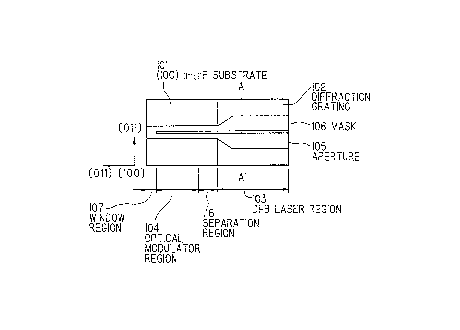
In fabrication, a diffraction grating 102 is
partially formed on an n-InP substrate 101, having a [100]
surface, to give a period of 240nm in a [011] direction and
a depth of 30nm. The area on which the diffraction grating
102 is formed is used as a DFB laser region 103, and part of
the remaining region is used as an optical modulator region
104. A SiO2 layer is formed on the substrate by a heated CVD
technique, and then a stripe-shaped aperture 105 with a
width of 2~m is formed by a photolithography and etching
technique. Then, a growth-preventing mask 106 is formed on
both sides of the aperture 105, the mask having a width of
17~m on the DFB laser region 103 and a width of 8~m on the
optical modulator region 104. The mask 106 extends in
parallel to the [011] direction of the n-InP substrate 101.
A window region 107 is formed on the substrate in an area
located 15~m from an end of the optical modulator region 107
by forming no aperture therein, as shown in Figure 3.
Subsequently, as shown in Figure 4A, by using a
low-pressure MOVPE apparatus, the following layers are
continuously MOVPE-grown on a stripe portion of the
CA 02139140 1998-06-09
substrate exposed from the aperture 105: a n-InGaAsP light
waveguide layer 108 having a wavelength composition of
1.15~m and a thickness of 100nm, a n-InP spacer layer 109
having a thickness of 40nm, an undoped multiple quantum well
layer 110 of 7 periods composed of an undoped InGaAsP
barrier layer having a wavelength composition of 1.3~m and
a thickness of 10nm and an undoped InGaAs well layer having
a thickness of 7nm, an undoped InGaAsP hole acceleration
layer 111 having a wavelength composition of 1.15~m and a
thickness of 40nm, and a p-InP clad layer 112 having a
thickness of 200nm. In this growth procedure, the N-InGaAsP
light waveguide layer 108, n-InP spacer layer 109, undoped
InGaAsP hole acceleration layer 111 and p-InP clad layer 112
are grown at a pressure of 25 Torr, but the undoped multiple
quantum well layer 110 is grown at a pressure of 150 Torr.
The growth condition is controlled so that the undoped
InGaAs well layer and the undoped InGaAsP barrier layer are
lattice-matched with the n-InP substrate 101 on the DFB
laser region 103. The undoped quantum well region 110 has
bandgap wavelengths of 1.55~m and 1.48~m on the DFB laser
region 103 and the optical modulator region 104,
respectively.
Next, as shown in Figure 4B, the aperture 105 is
expanded in width to 7~m and 5~m on the DFB laser region 103
and the optical modulator region 104, respectively, by
photolithography and etching processing. On the stripe
portion of the substrate exposed from the expanded aperture
105, an undoped InP field relaxation layer 113 having a
thickness of 40nm, a p-InP buried layer 114 having a
thickness of 1.4~m and a p+ InGaAs contact layer 115 having
a thickness of 200nm are selectively grown by the MOVPE
technique. In order to electrically isolate the DFB laser
region 103 and optical modulator region 104 from each other,
the p+ InGaAs contact layer 115 is partially removed 25~m
from the boundary thereof with the optical modulator region
to form a separation region 116, shown in Figure 3.
CA 02139140 1998-06-09
Next, as shown in Figure 4C, an insulation layer
117 is provided over the entire structure to a thickness of
0.3~m, then holes are shaped by a photolithography and
etching technique in the insulation layer 117 to expose the
p+ InGaAs contact layer. A Ti/Au electrode 118 is coated
and patterned by a photolithography and etching technique.
The n-InP substrate 101 is lapped to lOO~m, and then a Ti/Au
electrode 118 is coated on the rear surface thereof.
Consequently, a low-reflection coating and a high-
reflection coating are provided on the facets of the opticalmodulator region and the DFB laser region, respectively. In
this embodiment, each layer thickness represents a thickness
of a layer selectively grown on the aperture in the DFB
laser region.
In a thus-fabricated integrated light source, when
current is injected into the DFB laser region 103, single-
mode oscillation is performed at a wavelength which is
determined by an effective refractive index calculated on
the basis of the pitch of the diffraction grating 102 and
the cross-sectional structure thereof. The undoped quantum
well layer 110 (light-absorption layer) in the optical
modulator region 104 has a bandgap wavelength of 1.48~m in
order to restrain light absorption in a non-bias condition.
When a field is applied to the light-absorption layer, the
absorption coefficient for transmission light is increased
by QCSE (Quantum-Confined Stark Effect), so that the
structure can operate as a light intensity modulator.
When a 3V reverse voltage is applied to the
optical modulator region 103, the light-absorption layer is
biased by a high field of 200kV/cm, and the light absorption
coefficient for the 1.55~m lasing wavelength is thereby
increased by 4300cm~1 by the QCSE. A light-confinement
factor of the seven-layered well layer is 4~, so that an
extinction ratio of 15dB is obtained with a device 200~m
long.
CA 02139140 1998-06-09
Generally, when light is reflected at the output
facet of the optical modulator region, the light is
reflected back and forth in the optical modulator region 104
and is fed back to the DFB laser region 103. If this kind
of light feedback is dynamically changed in light-intensity
modulation, the waveform of a light signal, which has been
transmitted in an optical fiber in a long-distance
communication, is degraded by a spectral charping phenomena
in which lasing wavelength is fluctuated in the modulation
processing. In order to avoid this kind of problem, a
reflectivity of less than 0.1% is required at the output
facet of the optical modulator region; however, it is
generally difficult to obtain that reflectivity. According
to the invention, the window region 107 provides no light
confinement in the transverse direction, so that a light
supplied thereto spreads and extends to the facet of the
optical modulator region 104. Only light reaching the facet
surface at a 90-degree angle can be reflected and be re-
coupled to the optical modulator region 104, so that a
reflectivity of 0.1% can be easily realized with a
conventional low-reflection coating.
In the above-mentioned embodiment, the DFB laser
region 103 provides single-mode oscillation at 1.55~m of
lasing wavelength and 10mA of threshold current. This means
that the coupling efficiency between the DFB laser region
103 and the optical modulator region 104 is 100%, and over
10mW of output power is obtained from the facet of the
modulator region. The isolation resistance between the DFB
laser region 103 and the optical modulator laser 104 is
lokn~ which provides good electrical isolation with no
problems in practical use. When an 80km fiber transmission
line was tested in the 2.5Gb/s band with the invented
integrated light source, the wavelength charping phenomena
was sufficiently restrained that high-quality transmission
performance was realized.
CA 02139140 1998-06-09
Next, a second preferred embodiment according to
the invention is described in conjunction with Figures 5 and
6A to 6C. This embodiment involves a tunable type of DBR
laser. In fabrication, a diffraction rating 202 is
partially formed on a n-InP substrate 201 of a surface, to
give a period of 24Onm in a direction and a depth of 3Onm.
The area on which the diffraction grating 202 is formed is
used as a DBR, with one-half of the other area closer to the
DBR region being used as a phase control region 204 and the
other half being used as an active region 205. A Si02 layer
is formed on the substrate by a heated CVD technique, and
then a stripe-shaped aperture 206 with a width of 2~m is
formed by a photolithography and etching technique. Then,
a growth-preventing mask 207 is formed on both sides of the
aperture 206 to provide a width of 12~m on the DBR laser
region 203, a width of 8~m on the phase control region 204,
and a width of 17~m on the active region 205. The mask 207
extends parallel to the direction of the n-InP substrate
201, as shown in Figure 5.
Subsequently, as shown in Figure 6A, by using a
low-pressure MOVPE apparatus, the following layers are
continuously MOVPE-grown on stripe portion of the substrate
exposed from the aperture 206: a n-InGaAsP light waveguide
layer 208 having a wavelength composition of 1.15~m and a
thickness of 100nm, a n-InP spacer layer 209 having a
thickness of 40nm, an undoped multiple quantum well layer
210 of 7 periods composed of an undoped InGaAsP barrier
layer having a wavelength composition of 1.3~m and a
thickness of 10nm, and an undoped InGaAs well layer having
a thickness of 7nm, an undoped InGaAsP hole acceleration
layer 211 having a wavelength composition of 1.15~m and a
thickness of 40nm, and a p-InP clad layer 212 having a
thickness of 200nm. In this growth procedure, the n-InGaAsP
light waveguide layer 208, n-InP spacer layer 209, undoped
InGaAsP hole acceleration layer 211 and p-InP clad layer 212
are grown at a pressure of 25 Torr, but the undoped multiple
CA 02139140 1998-06-09
quantum well layer 210 is grown at a pressure of 150 Torr.
The growth condition is controlled so that the undoped
InGaAs well layer and the undoped InGaAsP barrier layer are
lattice-matched with the n-InP substrate 201 on the active
region 205. The undoped multiple quantum well region 210
has bandgap wavelengths of 1.51~m, 1.48~m and 1.55~m on the
DBR region 203, the phase control region 204 and the active
region 205, respectively.
Next, as shown in Figure 6B, the mask 207 is
continuously etched from the inside thereof for each 2~m to
expand the width of aperture 206. On the expanded aperture
206, an undoped InP spacer layer 213 having a thickness of
40nm, a p-InP buried layer 214 having a thickness of 1.4~m
and a p+ InGaAs contact layer 215 having a thickness of
200nm are selectively grown by MOVPE technique. In order to
electrically isolate those regions from each other, the p+
InGaAs contact layer 215 is partially removed 25~m from the
boundary portions of those regions to form a separation
layer 216, shown in Figure 5.
Next, as shown in Figure 6C, an insulation layer
217 is provided over the entire structure to have a
thickness of 0.3~m, then holes are shaped by a
photolithography and etching technique in the insulation
layer 217 to expose the p+ InGaAs contact layer. A Ti/Au
electrode 219 is coated and patterned by a photolithography
and etching technique. The n-InP substrate 101 is lapped to
100 ~m, and then a Ti/Au electrode 219 is coated on the rear
surface thereof.
Consequently, a low-reflection coating and a high-
reflection coating are provided on the facets of the DBRregion and active region, respectively. In this embodiment,
each layer thickness represents a thickness of a layer
selectively grown on the aperture in the active region.
In the thus-fabricated tunable DBR laser, when
current is injected into the active region 205, single-mode
oscillation is performed with a wavelength which is
CA 02139140 1998-06-09
determined by an effective refractive index calculated on
the basis of the pitch of the diffraction grating 202 and
the cross-sectional structure of the DBR region 203. When
current is injected into the DBR region 203, the lasing
5 wavelength changes, shifting toward a shorter wavelength in
discrete fashion in accordance with alternative-axis-mode
jumping, with a reduction of the refractive index due to the
plasma-dispersion effect. When the phase-matching condition
of light transmitting back and forth in the cavity is
10 controlled by adjusting the current supplied to the phase
control region 204, fine tuning is realized even within a
lasing wavelength which has changed in discrete fashion, and
therefore, a virtually-continuous tuning operation of the
lasing wavelength is realized.
In the tunable DBR laser, when 15mA of current is
supplied into the active region 205, a single-longitudinal-
mode oscillation is obtained with 15mW of maximum light
output. When 60mA of current is supplied into the DBR
region 203, 7nm of tunable range is achieved. Current is
20 simultaneously supplied into the phase control region 204,
and a virtually-continuous tuning operation of lasing
wavelength is realized.
Although the invention has been described with
respect to specific embodiments for complete and clear
25 disclosure, the appended claims are not to be thus limited
but are to be construed as embodying all modifications and
alternative constructions that may occur to one skilled in
the art which fairly fall within the basic teaching herein
set forth.