Note : Les descriptions sont présentées dans la langue officielle dans laquelle elles ont été soumises.
~t~ g~'
- W094/030~ PCT/US93/06713
--1--
HIGH ~K~u~NCY ELECTRONIC CIRCUIT FOR
LOAD BALLASTING
BACKGROUND OF THE INVENTION
The present invention relates generally to energy
manaqement systems for electric loads. Utility of the
invention is found in power supplies and in lamp ballasts,
such as used in the operation of discharge lamps, such as
high intensity discharge (HID) lamps. More particularly, a
high frequency electronic ballast circuit responsive to a
highly dynamic load is described. The ballast circuit
includes a transformer having primary and secondary flu~
paths to vary the flux, linking a secondary winding coupling
the ballast to a load; and, due to the varying flux linkage,
the transformer also isolates the ballast-circuit from the
operating dynamics of the load.
Discharge lamps such as fluorescent, mercury, metal
halide and high pressure sodium lamps are popular sources of
light because of their high efficiency in converting
electrical energy into light. For the high efficiency
operation of such lamps, a high efficiency ballast circuit
must be provided. Likewise, there are many applications in
which a power supply responsive to a highly dynamic load is
required.
Due to the highly dynamic characteristics of
operation of certain loads, which may change from an
effective open circuit to a very iow impedance close to zero
in a matter of nanoseconds, for example, upon ignition of a
HID lamp, high efficiency ballast circuits have been very
W094/03034 ~ C A 2 1 4 0 2 9 0 PCT/US93/06713
-- 2
expensive. The high costs of prior art high efficiency
ballast circuits are due to the requirements of expensive
circuitry for high speed current limiting with high power
ratings, which are necessary to construct ballast circuits in
accordance with conventional circuit designs.
Accordingly, there is a need for an improved ballast
circuit which can survive the hostile conditions imposed by
starting and running dynamic loads at high efficiencies, yet
which utilizes low cost components, such that the cost of the
improved ballast circuit is substantially reduced in
comparison to currently available ballast circuits.
Power supplies in many applications also experience
highly dynamic behaviour that requires complex control
mechanisms to prevent variations in output voltages. To
provide adequate control, many analog components are added to
provide regulation in each needed output. The introduction
of these analog regulators also introduces high losses, and
therefore, results in low efficiency. The high losses in the
output regulators also require large physical size to allow
dissipation of the heat generated in analog regulators.
SUMMARY OF THE INVENTION
These ballast and power supply needs are met by the
invention of the present application wherein a high frequency
electronic ballast circuit includes a transformer having a
primary winding which is coupled to a secondary winding via a
primary flux path from which flux can be diverted by a
W O 94/03034 C A 2 1 4 0 2 9 0 ' PC~r/US93/06713
secondary flux path including an air gap, preferably an
adjustable air gap. For one mode of operation, a portion of
the secondary winding is switched out of the circuit
including a connected load. Alternately, for another mode of
operation a resonance element is connected in circuit with
the load and a load driver operated around the resonance
frequency. The frequency of operation can be adjusted,
manually or v a a frequency control signal generated by a
signal source or feedback loop, for power control and for
stability. A conventional operating frequency of devices of
this type is in the range of 20-30 Khz, although the
invention is not so restricted and may be designed for
operation in frequencies in much broader range, estimated to
be between about 15 Khz and about 500 Khz.
Use of the transformer permits operation from a
rectified alternating current power source which can be
compensated by a high frequency power supply to present a
favorable power factor to the alternating current power
supply. The ballast circuit preferably includes catastrophic
transient protection to extend life expectancy of the high
frequency ballast circuit.
In accordance with one aspect of the present
invention, a high frequency ballast circuit for operating a
dynamic load, such as a discharge lamp, comprises a
transformer having a primary winding and a variable flux
linked secondary winding for connection to a load, or lamp.
Driver means are connected to the primary winding for driving
the transformer to operate the load, or a discharge lamp,
W094/03034 2i 4029~ PC~/U593/06713
connected to the secondary winding. The transformer
comprises a primary flux path coupling the secondary winding
to the primary winding and a secondary flux path having a
higher magnetomotive force (MMF) drop than the primary flu~
path.
In one embodiment of the present invention, the
secondary winding comprises first and second winding portions
interconnected in series to one another at a common secondary
winding intermediate tap. In this embodiment, the ballast
circuit further comprises flux sensor means coupled to the
secondary flux path and switch means for selectively
connecting the driver means across the secondary winding, or
only across one of the first and second winding portions.
The switch control means is connected to the flux sensor
means for operating the switch means as a function of the
flux passing through the secondary flux path.
The secondary flux path includes an air gap to
define the higher magnetomotive force drop. Preferably, the
air gap is adjustable to enable selection of the higher
magnetomotive force drop in the secondary flux path. In
addition, an auxiliary air gap is provided adjacent at least
a portion of the primary winding for better control of
leakage fluxes and to optimize power output for any given
transformer core size.
In another embodiment, a high frequency ballast
circuit further comprises resonance means connected to the
secondary winding of the transformer for defining resonance
for the circuit including the secondary winding, the
W094/03034 ' ~ ` ` ' PCT/US93/06713
resonance means and a load. The resonance means may comprise
a series resonant capacitor connected in series with the
secondary winding and a discharge lamp for defining a series
resonance frequency during operation of a connected discharge
lamp. Alternately or in addition, the resonance means may
comprise a shunt resonant capacitor connected in shunt across
a connected discharge lamp for defining a shunt resonance
frequency while a connected discharge lamp is extinguished.
In this embodiment, the driver means comprises
oscillator means for setting an operating frequency for the
load or lamp driver means. The oscillator means may be
operated at a substantially fixed frequency. Alternately,
the high frequency ballast circuit may further comprise
frequency control means for setting an operating frequency
for the oscillator means. The frequency control means may
comprise manually adjustable circuitry, a frequency control
signal source and/or a feedback loop connected to the
oscillator means.
Feedback frequency control is particularly
advantageous where the high frequency ballast circuit
comprises an alternating current to high voltage direct
current converter means for generating high voltage direct
current power for the driver means. The frequency control
means then, comprises a feedback loop from the converter
means .or va.ying the frequency of operation of the
oscillator means as a function of variations in the high
voltage direct current power.
: '
W O 94/03034 Y~i 4 02gU PC~r/US93/06713
-- 6
In accordance with another aspect of the present
invention, a high frequency ballast circuit is provided as a
power supply for a load, such as for operating a discharge
lamp or any other type of lamp or load requiring a
dynamically responsive power source, and, comprises a
transformer having a primary winding and a variable flux
linked secondary winding for connection to a load. Driver
means connected to the primary winding drives the transformer
to the load, or lamp, connected to the secondary winding.
Power supply means generate full-wave rectified power from a
supply of alternating current power. The full-wave rectified
power is used by the driver means for driving the transformer
to operate a load connected to the secondary winding.
The transformer may further comprise an auxiliary
winding with the ballast circuit further comprising a power
storage capacitor. First rectifier means are connected
between the auxiliary winding of the transformer and the
power storage capacitor, and second rectifier means are
connected between the power storage capacitor and the power
supply means for conducting power from the power storage
capacitor to the power supply means. This arrangement
partially smooths the full-wave rectified power to improve
the power factor for the power supply means.
The first rectifier means may comprise a half-wave
rec~ifier circuit or a full-wave rectifier circuit for higner
power requirements. The auxiliary winding is selected to
generate a voltage on the power storage capacitor which is a
fraction, for example, one-half, of a peak voltage of the
21~290
W O 94/03034 : ~ PC~r/US93/06713
-- 7
supply of alternating current power. To provide extended
life for the circuit, the power supply means may comprise
catastrophic transient protection means for protecting the
power supply from one catastrophic power surge over the
lifetime of the ballast circuit.
The catastrophic transient protection may comprise a
first varistor designed to protect against voltage surges
exceeding a first defined voltage level. Fusible circuit
means for opening at current levels above a first current
level, connected in series with the first varistor, and the
series combination being connected in shunt across an input
for the supply of alternating current power are provided. A
second varistor designed to protect against voltage surges
exceeding a second defined voltage level greater than the
first defined voltage level connected in shunt across the
input for the supply Gf alternating current power is a
further variation. The fusible circuit means may comprise a
section of electrically conductive foil on a printed circuit
board, preferably formed in a zig-zag or triangular wave
pattern.
It is thus an object of the present invention to
provide an inexpensive high frequency electronic ballast
circuit which is responsive to a highly dynamic load, and for
example, which can reliably withstand the hostile starting
and running conditions of HID and other lamps; tG provide an
- inexpensive high frequency electronic ballast circuit having
a transformer having a primary winding and a variable flux
linked secondary winding for connection to a load; to provide
' f ~
W O 94/03034 ~ 1 4 0 2 9 0 P~r/US93/06713
-- 8
an inexpensive high frequency electronic ballast circuit
which presents a favorable power factor to an alternating
current power supply for the ballast circuit; and, to provide
an inexpensive high frequency electronic ballast circuit
including transient protection from a catastrophic power
surge on an alternating current power supply for the ballast
circuit.
Other objects and advantages of the invention will
be apparent from the following description, the accompanying
drawings and the appended claims.
BRIEF DESCRIPTION OF THE DRAWING
Fig. 1 is an electrical schematic diagram of a high
frequency electronic ballast circuit fcr high intensity
discharge lamps in accordance with the present invention.
Figs. 2-5 illustrate transformers having variably
coupled secondary windings for use in the ballast circuit of
Fig. 1.
Fig. 6 is a schematic diagram of modifications of
Fig. 1 for configuration of an alternate embodiment of the
ballast circuit of the present invention.
Fig. 7 is an electrical schematic diagram of power
input and processing circuitry of the ballast circuit of Fig.
1.
Figs. 8-11 are waveforms of signals within the
schematic diagram of Fig. 7.
Figs. 12-15 illustrate operation of a ballast
circuit in a resonant model.
21402gO
PEA .
Fig. 16 is a sawtooth waveform for a frequency
control 25 signal source of Pig. 1.
In Figure 17, the transformer indicated at 17T is
as otherwise described herein and includes wind ing 106 with
additional taps. The resonating capacitor is shown at 17C.
Figure 18 is a detail of the stability network
showing pertinent interconnections with the circuit
components of Figure 19. Figure 18A is an e~aggeration for
purposes of illustration and esplanation and depicts the
waveform of the ripple voltage on the DC rail.
Figure 19 depicts a load ballasting circuit
including the active power factor correction circuitry
identified within the bos marked l9A. In the bos identified
by l9B, Jl is used for HPS only; J2 is used for MH only. The
DC coil and chassis ground connections of the circuit
segments are likewise indicated. In the power input segment
of the circuit relay RYl and capacitors Cll, C13, and C14 and
resistors R20, R22, R23, R34, R32 and R37 have values
determined by the line voltage. Values for other components
are dependent on load wattage, and/or type of lamp, if the
circuit is so utilized.
In Figure 20, the dynamic harmonic cancellation circuit
is indicated inside the dotted bos identified as 20A. The
diode D12 is optional and need not be used in certain applic
ations. Connections of the circuit signals to the-DC rail
are also indicated.
~140290
iL~ 'r~; ;L3
~JU- r~
- 9a -
Figure 21 is a simplified block diagram of the
dynamic harmonic capture circuit showing a current
transformer at 21T for sampling line current and the control
line 21L connected through a bandpass amplifier to a DC line
between the line rectifier and ballast circuit to adjust for
the average DC level. Figure 21A shows the frequency gain
and bandpass of the line current amplifier shown in the block
diagram of Figure 21.
Operation of the start up circuit is shown in
Figure 22, in which the circuit transformer, as described
above, is shown as 22T with winding WNEW. Pertinent circuit
parameter equations are also included. Iin is present only
when the ballast output stage is escited. The base current
into Q4 is the summation of Iin and ~Iin.
DETAILED DESCRIPTION OF THE INVENTION
A first illustrative embodiment of a high
frequency electronic ballast circuit 100 in accordance with
the present invention is schematically shown in Fig. 1.
Before the operation of the ballast circuit 100 of Fig. 1 is
described in detail, the transformer 104 for use in the
ballast circuit 100 having a primary winding 106 and a
variable flus linked secondary winding 108 will be described
with reference to Figs. 2-5.
Al~ ncL-~
1 4 ~ 2 9 0 p
IPtA'~ F_~ ,394
- 9b -
In most transformers, the primary winding and the
secondary winding are coupled as tightly as possible to
provide masimum energy transfer under all conditions. For
such masimum energy transfer, substantially all available
flu~ couples the primary winding to the secondary winding.
~ , . . :. c ~
2110290 P~; J ' - '`
IPEAiL)f~ G 4 F~ g i394
-- 10 --
If the frequency and applied primary voltage are constant,
the flus will have a constant peak and rate-of-change.
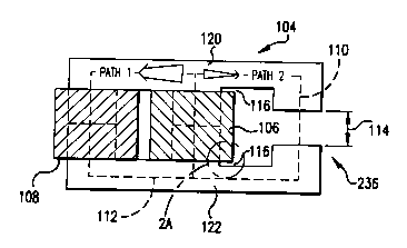
To make the secondary winding 108 variably coupled
to the primary winding 106, a secondary flus path 110 having
a higher magnetomotive force (MMF) drop than the principal
flus path 112 is provided. One transformer configuration is
shown in Figs. 2 and 3 wherein path 1, the principal flus
path 112, is the preferred flus path when no load is
connected to the secondary winding 108, e., when the load
or lamp 102 is nonconducting and thus on path 2, the
secondary flus path 110, is an effective open circuit. Path
2, the secondary flus path 110, has a large air gap 114 with
a high associated MMF drop.
Accordingly, nearly all of the flus generated by
the primary winding 106 is coupled into the secondary winding
108 and the resulting induced voltage is at a masimum such
that the peak voltage attains a value which will esceed the
breakover voltage of the load or lamp 102. The arrow widths
in Figs. 2-3 are indicative of the relative magnitudes of
magnetic flus in each path.
An ausiliary space or gap 116 may be provided
adjacent to the primary winding 106 on the control path or
secondary flus path 110, path 2 as shown in Figs. 2 and 3.
Figure 2A further illustrates the ausiliary gap 116 that is
contained in reference circle 2A. The ausiliary gap 116
provides better control of the leakage fluxes near the
2140290
P.~ J6 ~ ~3
, ~,
IP~G~F~
- lOa -
primary winding and optimizes power output for any given
transformer core size.
At the moment of transition of a dynamic load,
such as by the ignition of a lamp at 102, the MMF drop
through the
A~ ;H,r~
W094/03034 ~1 4 0 2 ~ PCT/US93/~713
secondary winding 108 becomes very high as the load or lamp
102, immediately after iqnition, is a very low impedance,
closely approximating a short circuit. Because of this
change in load impedance and MMF drop within path 1 (the
principal flux path 112) of the transformer 104, path 2 (the
auxiliary flux path 110) becomes a more attractive flux path.
The arrow widths in Fig. 3 schematically represent
the division of flux through the t.ansformer-core after
dynamic loading, i.e., ignition of the lamp 102. The smaller
flow of flux through the secondary that the voltage induced
into the winding 108 illustrates that secondary winding 108
is much smaller than under the pre-ignition or no load
condition. As the load or lamp 102 develops a higher
impedance, the flux divides so as to increase the flux into
path 1 and therefore the load or lamp voltage increases to
match the higher impedance with a voltage that maintains a
substantially constant current into the load 102. The air
gap 114 shown in Fig. 2 controls the coupling strength for
the secondary winding 108 and therefore the final
equilibrated power delivered to the load 102.
The core of the transformer 104 can be manufactured
with a specific dimension for the gap 114 to obtain a
specific power level for the load 102. Alternately, the core
configuration shown in Fig. 5 can be used wherein a moveable
end piece 118 allows adjustment of power levels during
preliminary ballast setup, or as a way of variably
controlling the load power level over the lifetime of the
ballast circuit 100, or in lamp applications, the lifetime of
- W094/03034 214 0 2 ~ ~ PCT/US93/06713
- 12 -
a given lamp load, such as lamp 102. For example, the
moveable end piece 118 of the core of the transformer 104 of
Fig. 5 permits selection of an air gap 114A or 114B with
corresponding power levels.
In the illustrated embodiments of Figs. 2-5, the
transformer 104 is constructed using E-shaped cores 120 and
122. Other core configurations can be utilized in
constructing transformers having variable flux linked
secondary windings for use in the ballast circuit 100 as will
be apparent to those skilled in the art. Further, placement
of the primary 106 is not limited to the center leg of
transformers using the E-shaped cores.
For example, Fig. 4 shows a transformer
configuration wherein the primary and secondary windings 106
and 108 are on the outer legs of the transformer core with
the control air gap 114 being formed on the center leg. The
transformer configuration of Fig. 4 changes the two magnetic
flux paths 110, 112 as shown. The configuration of Fig. 4
would provide better magnetic containment but would be more
difficult to adjust during manufacture.
Alternately, the primary winding 106 can be on one
outer leg, the secondary winding 108 on the center leg with
the other outer leg including the control air gap 114 as
shown in Fig. 5. A great variety of configurations beyond
those illustrated will be apparent to those skilled in the
art.
The operation of the high frequency electronic
ballast circuit 100 of Fig. 1 including a transformer having
W O 94/03034 2 1 4 U ~ ~ O PC~r/US93/06713
a primary winding and a variable flux linked secondary
winding will now be described. Two modes of operation, a
resonant mode and a switched secondary mode, will be
described with reference to Figs. 1 and 6, respectively.
In Fig. 1, a capacitor 124 is connected between the
variably flux linked secondary winding 108 and the lamp or
load 102. The capacitor 124 resonates the load circuit
during operation of the load 102 in a series resonant mode.
The effective resistance of the load 102 controls the Q,
quality factor, of the resonant condition to give the
resonant response a broad frequency range between the half
power points. Such a broad frequency range is significant
because the normal variations in operating frequencies due to
component and thermal variations can be as high as 3% to 6%
which would cause severe out-of-tolerance operation if the
load circuit had a high Q and narrow frequency range.
A capacitor 126 may be used to resonate the load
circuit prior to application of a load, such as by ignition
of a lamp at the load position, 102, to provide voltage and
frequency peaking to accelerate ignition of the lamp 102.
The frequency of the parallel resonance due to the capacitor
126 is higher than the frequency of the series resonance due
to the capacitor 124. When used in a lamp application, the
parallel resonance takes advantage of the inverse
relationship of frequency tc ignition voltage in gas lamps,
e. the higher the frequency of voltage applied to a gas
lamp, the lower the level of the voltage required for
ignition of the lamp. Use of the parallel resonant capacitor
21402gO
- W094/03034 PCT/US93/06713
- 14 ~ ~ r~
,
126 is not necessary or currently preferred for low wattage
high freguency electronic ballast circuits of the present
invention.
In the resonant mode of operation of the ballast
circuit 100 of Fig. 1, the transformer 104 having a variably
flux linked secondary winding 108 operates in what is
referred to herein as a fully compliant mode. UCompliant'' as
used herein is the ability of a device to drive a load to
deliver the needed voltage to allow the load to continue to
operate under normal operating conditions. "Fully compliant"
as used herein means that the device used to drive a load or
lamp is able to first generate the high voltage required for
a start or ignition, and then to drop to a low voltage during
the warm up phase of operation, while preventing the lamp or
load from extinguishing such that it must be once again
ignited or restarted.
Driver means 128 is connected to the primary winding
106 for driving the transformer 104, the lamp 102 connected
to the secondary winding 108. The driver means 128 can be
any switching type drive circuit capable of driving the
transformer 104 and lamp or load 102 at sufficiently high
frequencies at or around 28.5 Khz. However, in the
illustrated embodiment of Fig. 1, the driver means 128
comprises a pulse width modulation (PWM) circuit 130 which,
in its simpiest mode of operation, operates as an oscillator
to control a driver circuit 132 which drives a pair of
insulated gate bipolar transistors (IGBT's) 134, 136.
W 094/03034 ~ P(~r/US93/06713
21 ~ 02 g ~ - 15 _
For esample and as illustrated, the pulse width
modulation (PWM) circuit 130 may comprise an SG3526
(commercially available from Motorola Corporation) and the
driver circuit 132 may an IR 2110 integrated driver circuit
(commercially available from the International Resistor
Corporation). The use of the PWM circuit 130 permits
frequency control or modulation of the drive signal for the
lamp or load at 102 and back-up current and power controls
for the ballast circuit 100.
For esample, current through the primary winding 106
is sensed by monitoring the voltage across a current sensing
resistor 142. The masimum current level is set by a
potentiometer 144 which is connected to a current limit input
on the PWM circuit 130. Current sample pulses from the
sensing resistor 142 are also passed to resistors 146, 148
which determine the gain of an operational amplifier internal
to the PWM circuit 130 and set up as an integrating/error
amplifier. A capacitor 150 connected to the PWM circuit 130
integrates the current sample pulses into a direct current
(DC) voltage level for comparison to a preset reference level
to generate an error signal voltage. The preset reference
level is generated by resistors 146, 148 which are selected
to define ultimate lamp or load power through operation of
the PWM circuit 130. While these controls are not utilized
during normal operation of the ballast circuit lG0, they can
function to protect circuit elements in the event of failures
within the circuit.
- W 094/03034 2 1 4 0 2 g O ` PC~r/US93/06713
- 16 _ ~ t~
The illustrated driver circuit 132 provides level
shifting in one drive such that only one drive needs to be
referred to ground potential. The floating drive is attached
to the transistor 136. Energy to operate the floating drive
is stored on a capacitor 152 and is conducted through a
resistor 154 and a diode 156. When the transistor 134 pulls
its drain to ground potential, its source is nearly at ground
level. Because the diode 156 is tied to a low voltage supply
and the source of the transistor 136 is near ground level,
the capacitor 152 will charge to the low voltage supply minus
any voltage drops across the diode 156 and the transistor
136. The resistor 154 limits the rate of current rise to
acceptable levels. The transfer of current pulses into the
gates of the transistors 134, 136 require good bypassing at
the drive circuit 132, which is accomplished by capacitors
152, 158.
The illustrated driver arrangement would be
classified as a half-bridge configuration. The transistors
134, 136 are the active power switches and capacitors 160,
162 provide the passive coupling to complete the drive
configuration. Diodes 164, 166 provide for the inductive
return of energy stored in the inductances of the transformer
104.
The operation of the driver arrangement is as
follows:
1) The transistor 134 receives drive voltage and
saturates.
W094/03034 2 1 4 0 2 9~ PCT/US93/06713
2) Current flows through the capacitor 160, the
primary winding 106 of the transformer 104, and
then to the drain of the transistor 134.
3) The driver terminates in the transistor 134.
4) Current flow transfers to the diode 164 as the
transistor 134 turns off, and begins to decay.
5) A length of dead time will occur with the dead
time being set by the resistor 168 connected to
the PWM circuit 130. The dead time allows each
of the transistors 134, 136 to fully turn off
before the nest one turns on.
6) The transistor 136 now receives drive voltage
and saturates.
7) Current flows through the capacitor 162,
reverses in the primary winding 106 of the lamp
transformer 104, and then the drain of the
transistor 136.
8) The drive terminates in the transistor 136.
9) Current flow transfers into the diode 166 as
the transistor 136 turns off, and begins to
decay.
10) After the dead time, the transistor 134 begins
the cycle once again.
Resistors 170, 172 with a capacitor 174 filter the
sampled current pulses to remove unwanted transients that
could cause a false current trip. Capacitors 176, 178 bypass
an internal reference source and the low voltage supply,
respectively. A resistor 180 maintains a reset input of the
- W094/03034 ~1 4 0 2 9 Q . ~ PCT/US93/06713
- 18 -
PWM circuit 130 high to enable normal operation. A capacitor
182 controls the ramp-on rate of the pulse output from the
start-up condition.
One aspect of the high frequency ballast circuit 100
of the present invention is that it can be operated by an
unfiltered or other uneven input voltage. The reason it may
be desirable to operate with an unfiltered input voltage is
that the use of such an input voltage substantially prevents
line pulse current and associated poor power factors when a
rectified input voltage is filtered to obtain a clean DC
voltage. Two approaches to use of an unfiltered input
voltage are disclosed herein.
In Fig. 1, a full-wave bridge rectifier 184 is
illustrated. A capacitor 186 is sized to perform noise
reduction but not any appreciable level of energy storage.
The waveform of the resulting output voltage accordingly is a
full-wave rectified sine wave which is used to power the
drive arrangement for the transformer 104 described above.
When such an input voltage signal is used, the lamp or other
load at 102 is maintained in its conductive state by the
variable flus coupled secondary winding 108 of the
transformer 104 as previously described.
As the voltage falls, the flus coupling the primary
winding 106 to the secondary winding 108 remains relatively
constant at very close to the zero crosspoint, thus
maintaining stable operation. Unfortunately, direct use of
the full-wave rectified sine wave as the input drive voltage
places high dynamic constraints on the design of the
W O 94/03034 ~ 1 g 0 2 9 0 PC~r/US93/06713
-- 19 --
magnetics and thus requires a larger transformer core
cross-sectional area than would be required if the input
voltage source was well filtered. This problem can be
corrected by use of an ausiliary high voltage drive
arrangement which will nest be described.
Reference should also be made to Figs. 7-11 in
addition to Fig. 1 for the following description.
Fig. 7 illustrates a portion of power supply means
used in the ballast circuit 100 while Figs. 8-11 show
waveforms within the portion of the power supply means of
Fig. 7. A power rectifying diode 188 and a capacitor 190 are
connected to an ausiliary winding 192 of the transformer
104. The voltage output from the ausiliary winding 192 is
selected to be less than the peak of the input voltage level
of the AC line power, preferably about half, and is rectified
by the diode 188 and stored by the capacitor 190. Dependent
upon the power level of the electronic ballast circuit 100, a
second rectifying diode 194 can be provided for full-wave
rectification. See Figs. 1 and 7. A diode 196 isolates the
capacitor 190 from the capacitor 186 when the line voltage is
higher than the ausiliary source voltage developed on the
capacitor 190. This has the effect at the line of
introducing a small harmonic distortion, less than 104, and
achieves a power factor of 88%-92%.
The waveform of the input current I, shown in Fig. 9
is typical of the kind of distortion that is espected when
the DC power generated by the high frequency output from the
auxiliary winding 192 is combined with the full-wave
21~02g~
- W O 94/03034 PC~r/US93/06713
J~,.
rectified signal VO' shown in Fig. 10, generated by the
full-wave bridge rectifier 184. Fig. 11 shows the resulting
voltage waveform VO' on the high voltage DC rail of the
ballast circuit 100. While the result is substantially less
than complete filtering, its effect minimizes the magnetic
design so that the design is no worse than if the DC rail
voltage is well filtered. The size of the capacitor 190 is
substantially smaller than the capacitor that would be needed
if the DC rail supply was filtered in a conventional manner.
The energy stored on the capacitor 190 is supplied during
times when the absolute, value of the input line voltage is
less than the voltage on the capacitor 190.
In the resonant mode of operation, the capacitive
reactance and the inductive reactance of the lamp or load
circuit (the capacitor 124, the secondary winding 108 and the
load 102) sum to zero at the resonant frequency providing an
impedance minima or a current maxima. Operation precisely at
resonance is not desirable since the resulting impedance is
that of the lamp or load resistance only and will produce a
square wave current in the output stage. It is currently
preferred to operate the ballast circuit 100 at a frequency
just below resonance with a resulting effective impedance
that is capacitive in nature. Such operation produces, in
effect, an electrical-inertial voltage source that at any
nstance must be summed with the DC rail voltage to obtain
the net drive voltage.
Operation of the ballast circuit on the lead side of
resonance leads to the flux density in the core increasing
W094/03034 PCT/US93/06713
214029~ 21 -
with increasing frequency up to the resonant frequency fr as
shown in Fig. 12. This positively sloping frequency to flux
density curve permits the preferred operation of the ballast
circuit in the resonant mode. Since the flux density is a
positive function of frequency and voltage up to the
resonance frequency fr~ the drive frequency can be modulated
to keep the core flux density substantially constant in spite
of ripple on the DC rail high voltage.
The high voltage of the DC rail is shown in Fig. 13
with the ripple voltage indicated by /\V. The variation in
flux density with no control of the lamp or load drive
frequency by feedback is shown in Fig. 14 and is indicated by
/\B. As shown in Fig. 15, the core flux density is
maintained at a substantially constant level by controlling
the frequency of the lamp or load drive signal in response to
feedback from the power supply of the ballast circuit 100.
The core flux density can be held constant over a large range
of DC rail variations.
Generation of a feedback signal is performed from
the low voltage power supply such that the feedback signal is
reduced in amplitude yet proportional to the ripple on the
high voltage rail.
The low voltage supply also forms a part of the
present invention and its operation will now be described
prior to completing the description of tne frequency control
of the ballast circuit 100.
When AC line power is applied to the ballast circuit
100, a capacitor 198 is charged through a resistor 200. Once
2t ~02~0
- W094/03034 PCT/US93/06713
- 22 -
the voltage on the capacitor 198 reaches approximately 20
volts, a silicon bilateral switch 202 becomes conductive and
remains conductive until the ballast circuit 100 is turned
off. The power stored in the capacitor 198 sustains
operation until voltage is induced in a low voltage secondary
winding 204 to sustain normal operation. Current flows
through the silicon bilateral switch 202 and a resistor 205
to the parallel combination of a zener diode 206 and energy
storage capacitor 208, which serve to maintain a supply of
low voltage power having a voltage level defined by the zener
diode 206.
As shown in Fig. 1, resistors 210, 212 and capacitor
214 are used to generate the feedback signal for frequency
control within the ballast circuit 100. The capacitor 198
acts as an integrator of the cycle to cycle current charging
the capacitor 214. The junction of the resistors 210 and 212
is connected to the timing control pin 9 of the PWM circuit
130. As the voltage rises at the unregulated side of the
resistor 205, the frequency of the drive signal for the
ballast circuit 100 is reduced thereby substantially
canceling the effect of the increasing driving voltage on the
core flux density. Conversely, the frequency of the drive
signal is increased as the voltage falls.
The relationship between the frequency of the drive
signal in the ballast circuit 100 and the flux density in the
core of the transformer 104 as shown in Fig. 12 is thus seen
as providing a means for controlling power delivered to the
lamp or load 102 by frequency control within the ballast
. ~.
W 094/03034 2 1 ~ 0 2 9 0 PC~r/US93/06713
- 23 -
circuit 100. While the feedback from the resistors 210, 212
provides an automatic control of the frequency of the drive
signal as earlier noted with reference to Figs. 13-15,
frequency control can also be initially calibrated using a
potentiometer 216 in combination with a capacitor 218.
The frequency of the drive signal can also be
continuously varied about a given operating frequency for
ensuring a stable arc at the given operating frequency. For
such continuous frequency variation, a frequency control
signal source 219 can be provided alone or together with the
feedback frequency control as previously described. The
signal source 219 is shown in dotted lines in Fig. 1 since it
is optional for the ballast circuit 100. One waveform which
can be used for the signal source 219 is illustrated in Fig.
16 as a triangular or sawtooth waveform fs and should have a
frequency greater than the AC power line frequency but less
than the operating frequency of the ballast circuit 100.
Temperature compensation is preferably performed
using a series combination of a resistor 220 and a
temperature compensated resistor 222 sold commercially under
the trademark "Tempsistor~ by Midwest Components, Inc.
Finally, frequency control can be performed manually, for
example to control the load power level, by means of an
optoisolator 224 which can be controlled via a voltage
control device 226. An appropriate optoisolator can be
selected from a family of optoisolators commercially
available as the ~HllF~ family.
21402gO
- W094/03034 ~ J~ ~ PCT/US93/06713
- 24 -
As previously noted, other control functions on the
PWM circuit 130 are now used for limiting purposes only.
Components connected to pins 1, 2 and 3 are used as an
average current limit control to limit the maximum power
attainable by the ballast circuit 100. Current limiting
inputs on pins 6 and 7 are used as a backup for limiting the
average drive current for the transformer 104.
An alternate mode of operation is performed by a
modified version of the ballast circuit of Fig. 1. For ease
of illustration and description, only the modification to the
circuit of Fig. 1 is illustrated and described herein with
reference to Fig. 6. As with the resonant mode of operation,
this alternate mode of operation makes the transformer 104A
fully compliant by insertinq a large inductance in series
with the lamp at the load position 102. While making
operation rully compliant, unfortunately it also creates a
triangular current waveform in the output stage which is not
ideal and will not allow the output stage to produce the
maximum power throughput given the current ratings of the
transistors 134, 136.
While correction of the triangular current waveform
was by resonant operation in the illustrative embodiment of
Fig. 1, in the embodiment of Fig. 6, correction is performed
by switching out a large part of the inductance, i.e. the
secondary winding, after load application, such as by the
ignition of a lamp. Such switching removes much of the
inductance in series with a lamp at the load position 102 and
provides a more square drive current waveform at the output
W094/03034 !' ;s ~, ,, PCT/US93/06713
- 25 -
stage. To this end, the secondary winding 108A includes a
first tap 228 and a second tap 230. A relay comprising a
coil 232 and a controlled contact 234 selects either the
first tap 228 for starting or the second tap 230 for running.
The operated/released state of the relay is
determined by sensing the flus level in the secondary flux
path 110 defined by a section 236 of the transformer core
which includes the control air gap 114 as shown in Figs.
2-5. As the flux density increases above a preset level, the
relay driver 238 operates the relay to switch to the running
or second tap 230 to continue operation. Ps shown in Fig. 6,
a sense winding 240 is coupled to the core section 236.
Before application of a dynamic load, little flux flows in
the core section 236; however, after loading, substantial
flux flows to thereby induce an activating voltage level in
the sense winding 240. The resulting AC voltage is rectified
by a diode 242 and filtered by a parallel combination of a
capacitor 244 and a resistor 246. The relay driver 238
comprises a comparator which operates the relay when the
voltage generated by the sense winding 240 exceeds a
threshold voltage defined by resistors 248, 250.
By switching out a section of the secondary winding
108A, and thus reducing the inductance connected in series
with the load 102, the current waveform will take on a square
shape such that the power throughput for a given maximum
transistor peak current is nearly 60% greater.
In another aspect of the present invention, the AC
power line input, as shown in Fig. 1, is configured to
- W O g4/03034 2110~90 : PC~r/US93/06713
- 26 -
protect the ballast circuit against one catastrophic power
transient. As shown, a first varistor 252 is connected
across the line in series with a fuse 254, a first inductor
256 and a zig-zag foil film section 258 preferably formed as
a part of a printed circuit board, but not in series with a
second inductor 260. A second varistor 262 is connected
across the line in series with the fuse 254, and both
inductors 256 and 260. Accordingly, the second varistor 262
has a higher impedance in series with it than the first
varistor 252 such that the first varistor 252 will first
engage any transient energy appearing on the input for the AC
line power.
If the transient energy is sufficiently hiqh so as
to be catastrophic for the ballast circuit 100, the transient
current will burn off the zig-zag foil film section 258 as it
is diverted by the first varistor 252 which greatly enhances
the energy dissipation ability for the one time occurrence.
After the occurrence of such a catastrophic transient, the
second varistor 262 remains intact to act in a more
traditional protection manner.
The system has general applicability to dynamic
laods as a power supply, as well as to discharge lamps.
Figures 17-22 show additional embodiments.
To provide for a regulated output voltage, the
secondary lC8 ir. Figure 17 is resonated without the load or
lamp in place. This will provide a constant volts-per-turn
when the unit is operated as described in the main embodiment
described above. Figure 17 is a typical power supply
I ~t,~
W O 94/03034 X 1 ~ 0 ~ ~ U PC~r/US93/06713
- 27 -
configuration where there is a need for multiple voltage
output configuration. A tap of winding 108 is selected to
provide the proper voltage output after rectification by
bridge rectifier BRl and BR2, and filtering by Cl and C2
respectively. The use of two sources here is illustrative
and does not imply in any way that two is a limit of the
number of sources. Determined by design, need, or
predetermined application. There could be any number of taps
and sources. Regulation over any load variation is provided
by the very low impedance looking back into the secrondary,
which is in the order of 1 to 10 milliohm. To compensate for
bridge input voltage variation, each tap is therefore
regulated by the frequency modulation that occurs. However,
each source is regulated not by compensation with the excess
voltage that would be applied to an analog regulator, as in
an ordinary power supply, but rather by making the internal
voltage source invariant and very low impedance. For
esample, in a computer power supply, this not only allows a
volt +S high current source, but also enables the auxiliary
voltage sources to draw high power without reducing
efficiency or increasing physical size.
An alternative start up circuit is shown in Figure
19 which corresponds to the functional drawing shown on
Figure 22. When the circuit is not active and voltage is
applied at V in~ transistor Q9 is biased on by the current
induced in resistor RStart~ This bias current is referred to
as Iin. Q9 is driven into saturation and current flows in
RStart to initialize the operation of the circuit. When the
214U'~9O
- W094/03034 !s~ PCT/US93/06713
- 28 -
bridge becomes active winding WneW will now have an induced
voltage that will set up a voltage source that will negate
the bias current into the base of Q9. The base emitter will
not be reverse biased. The winding is adjusted so as to
prevent the base emitter from being driven into a zener
mode. Q9 is removed from conduction and the transistor is
now turned off and current no longer flows in RStart~ This
terminates the initialization or start-up sequence.
As heretofore explained, one embodiment of the
circuit uses an internally generated voltage source to
improve the overall power factor of the circuit; however, the
internal source generates a high level of harmonics on the
line. Certain markets and applications require that the
power factor be better than 96% and the THD lower than 30%.
A circuit configuration called the Dynamic Harmonic
Consultation circuit (DHC) overcomes this problem of
harmonics generation. This configuration is an "integrated
topology" because the same power output stage that drives the
output transformer is also responsible for power factor
correction and harmonic control, in contrast with a circuit
that uses a separate circuit that corrects first for line
dynamics and a second that provides the ballast or power
supply function.) Figure 21 is a block diagram of DHC
configuration.
In Figure 20, current transformer CTl samples the
- line current that is then fed into a bandpass-limiting
circuit to ensure that very little of the 60 hertz signal
passes through. The phase of the remaining harmonics are
W O 94/03034 ;, ~ P(~r/US93/06713
2140290
- 29 -
then fed into a summing junction that sums the control signal
that also compensates for the average level of the DC rail
and the phase-inverted harmonics. The bandpass-limiting can
be as simple as a first order RC filter or a more precise
second order active filter. The ideal bandpass is shown in
Figure 21. In theory, none of the 60 Hertz energy would pass
the filter. Practically, though, some of the fundamental
harmonics do pass through, and this proves to be the limiting
factor for the effectiveness of the DHC. This method is far
more effective because the output stage is the load on the
rectified line input. The way the output stage draws current
is modified so as to not create harmonics on the line that
would then be captured by the input sampling circuit. The
harmonics that are present are actually the error signal in
the control loop. They are, however, quite small and
correction to less than 14% THD has been demonstrated.
A circuit embodying the high frequency electronic
ballast of the iniation and achieving DHC is shown in Figure
20. The components in the blocked area are those responsible
for DHC. Current transformer CTl samples the line current
with full fidelity of harmonics. R12, Zl and Z2 provide for
pulse limiting during startup and other transient line
conditions. Diodes D4, D5, D9 and D8 mirror the input
rectifiers' offsetting effect on the harmonics. Capacitor C5
reduc~s noise sisnals above the desired capture frequency.
C9, C10 and R20 configure the op-amp's bandpass as specified
earlier. The output of this amplifier is taken at pin 1.
W O 94/03034 ~ 1 4 ~ 2 ~ O PC~r~US93/06713
- 30 -
D10, R21 and R24 allow the control signal to be asymmetric
and improve the overall performance of the DHC.
Other than the reduction of harmonics, the DHC also
provides a more precise control voltage for compensating the
output voltaqe at the load.
In certain embodiments, a notching of the input line
current occurs as the sine function nears the zero cross
point. This interval of time also sees a large ripple
voltage on the DC rail that is compensated for by a frequency
shift that results in an elimination of that ripple in the
secondary output. An improvement of this function is
achieved by the circuit shown in the blocked area of Figure
20. This improvement speeds up the response time of the
ripple compensation. In Figure 20, R7 and R16 set up a high
gain in amp B of the dual op-amp shown. R27 and C2 improve
the rise and fall time of the resulting control signal. The
resulting output is a square wave that occurs during the line
notch. Diode D12 and Dll isolate the oscillator input when
the op amp output is high. When the line notch occurs the op
amp goes low and the voltage across R28 drops below the anode
voltage of D12. Diode D12 forward biases and effectively
connects R28 to the oscillator input resulting in an increase
in frequency and the levelling of the secondary voltage.
Another variation of the circuitry utilizes a
standard boost-topology power factor correctiol.. A variation
of the circuitry, especially when applied as a ballast for
discharge lamps, is seen in Figure 19. Here the ballast uses
a commercially available active power factor corrector
2140290
W O 94/03034 PC~r/US93/06713
- 31 -
circuit, UC3852, for power factor correction and reduction of
line harmonics. The operation of this circuit is precisely
as described by the manufacturer in the application sheets.
The functional chanqe in this variation is the introduction
of a frequency modulation that is not an inherent part of the
normal ballast operation. This is introduced by components
C26, R52, R35, C2 and J3 (a jumper makes this connection
optional). In normal operation, there is an always an amount
of ripple. Although this ripple is very low as compared to
the overall voltage level, it is more than enough to
introduce a significant deviation of frequency when used at
the frequency control input. Capacitor C2 couples the ripple
portion of the DC rail into voltage divider composed of R35
and R25. The attenuation can be modified for particular
stability and lamp geometry by this divider. The deviation
introduced is a smooth variation occurring at twice the line
frequency.
A second type of variation can be introduced by
placing jumper J3 instead of coupling capacitor C3. This
connects the attenuated signal to the UC3852 drive output.
The drive output has a frequency shift predicated on power
throughput and line cycle variation. This frequency provides
a randomizing effect of the main ballast frequency which is
preferred by some lamp geometries. A third deviation
strategy is to use both s...ooth and randomized together. The
connections are further exemplified in Figure 18.
Having thus described the invention of the present
application in detail and by reference to the preferred
2140290 : -
- W094/03034 PCT/US93/06713
embodiments thereof, it will be apparent that modifications
and variations are possible without departing from the scope
of the invention defined in the appended claims.