Note : Les descriptions sont présentées dans la langue officielle dans laquelle elles ont été soumises.
,~ Wo 94Jo~g73 ~ 3 3 Pcr/~lS93/08083
LASER ~YRO HIG~I VOLTAGE START MODULE
AND ~IIGH VOLTAGE PULSE GENERATOR
This invention relates generally to laser gyros and, more particularly, to a method
and apparatus for starting a laser gyro with high voltage generated within the housing
containing the laser gyro from a low voltage supply.
BACKGROUND OF THE INVENTION
Ring laser angular rate sensors, often re~erred to as ring laser gyros, are wellknown. One example of a ring laser angular rate sensor is U.S. Patent No. 4,751,718
issued to Hanse, et al., which is incorporated herein by reference. Present day ring laser
10 angular rate sensors include a thermally and mecbanically stable laser block having a
plurality of interconnected formed cavities. Mirrors are placed at the extrernities of the
cavities for reflecting laser bearns and providing an optical closed-looped path.
Prior art high voltage power supplies for laser gyros used a 2,500VDC large
extemal power supply placed outside of the laser gyro housing. The external supply
15 required high voltage feed-throughs into the laser gyro housing through a high voltage
feed-through connector. Such high voltage feed-throughs are expensive. Such highvoltage feed-through connectors are also difficult to construct while still maintaining a
hermetic seal for the laser gyro housing. Existing high voltage plastic seals can only
maintain a vacuum to 10~ Torr. In contrast, relatively inexpensive low voltage
20 connector seals can handle a 10 9 Torr herrnetic seal.
It is, therefore, one motive of the invention to provide a laser gyro incorporating
voltage supply lines that can utilize an inexpensive, herrnetic connector.
S13MMARY OF ~l ~; INVENTION
The invention provides a laser gyro high voltage start circuit including a high
25 voltage pulse generator and high voltage module that allow the external gyro voltage
supply to provide low voltages of +SVDC and +lSVDC, with an inexpensive hermeticconnector. The high voltage pulse generator arnplifies a five volt pulse at 60KHz duty
cycle to provide an output of 280 volt pulses at approximately a 50% duty cycle. The
high voltage pulse generator features ~lrst and second transistors for sbaping an output
30 waveform. The high voltage pulse generator uses a PN juncdon high voltage diode with
a high forward voltage drop and a resistor divider to drive the first transistor while
holding the first transistor out of saturation. The high voltage pulse generator also uses
a low voltage diode to create a dead band such that the first and second transistors are
wo 94/0~973 ~ 1 4 0 4 :~ ~ PCI /US93/08083
` 2
never on at the same time. The high voltage module comprises two high voltage
blocking diodes which protect the laser gyro active current control circuitry during start
up. Two small ballast rcsistors and a parallel lO times voltage multiplior provide an at
least 2500 VDC ou~ut. The high voltage start circuit is configured to be contained in '
S a volume which is smaller than the volume of a ring laser gyro block.
Other objects, features and advantages of the present invention will become -
apparent to those skilled in the art through the Description of the Preferred Embodiment,
Claims, and Drawings herein wherein like numerals refer to like elements. ~
BRIEF DESCRIPTlON OF THE DRAWINGS `
Figure 1 shows a block diagram of one embodiment of a ring laser gyro
employing the novel features of the present invention.
Figure 2 schematically shows a circuit diagram of one example of an active -
current control circuit made in accordance with the present invention.
Pigure 3 schematically shows a block diagram of one embodiment of a high
voltage start circuit æ provided by one aspect of the invention.
Figure 4 shows a detailed circuit diagram of a high voltage pulse generator
circuit as provided by one aspect of the invention.
Figures SA and 5B show high voltage pulse generator waveforms.
Figure 6 shows a circuit schematic diagram of a high voltage module of the
invention.
Figure 7 shows an alternate embodiment of the invention to provide an active
current control.
DESCRIPrION OF T~ PREFERRED EMBODIMENT
Referring now to Figurc 1, a schematic block diagram of one embodiment of a
ring laser gyro employing the novel features of the present invention is shown. The
present invendon will be explained by way of example embodiments. Those skilled in
the art having the benefit of this disclosu~e will apprcciate that the exarnples herein are
by way of illustradon of the principles of the invention and not by way of limitadon.
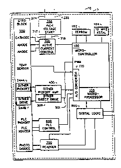
Ring laser gyro 10 includes a controller 100, a ring laser gyro block 200, an
active current control 300, dither pickoff amplifier 400, direct digital dither drive 500,
a path length control (PLC) device 600, a readout 700, and digital logic 800. The laser
gyro 10 further comprises a high voltage start module 3~0 providing power to the laser
block 200 and acdve current control 300. The controller 100 may be a rnicroprocessor
~i ;ï 94lO~973 ~ 1 g li 4 ~ ~ PCI /US93/08083
or microcontroller. One useful rnicrocontroller is the Intel model 80C196KC.
Referring now to Figure 2, a more detailed circuit diagram of one example of an
active current control apparatus is shown. The gyro block 200 is ill~strated as a
triangular bloclc having two anodes 201A, 201B and a cathode 203. Those skilled in
5 the art will understand that the ring laser gyro block can comprise other polygonal
shapes, such as rectangular. Those skilled in the art will also recognize that various
combinations and numbers of electrodes including anodes and cathodes may be used in
the ring laser gyro without departing from the scope of this invention.
The laser gyro of one embodiment of the invention includes an active current
10 control apparatus. The active current control apparatus 300 in this example includes
first, second, third and fourth amplifying means 312, 314, 324, 326, first and second
output transistor means 310, 316, first and second field effect transistor (~ET) means
320, 321, DC/DC conversion means 328 and high voltage start circuit means 350. The
active current control apparatus 300 is coupled to controller 100 and the ring laser gyro
block 200.
The fourth arnplifying means 326 is coupled to a gain resistor 327 at its inverting
input. Also coupled to the inverting input are four input resistors 370, 372, 374 and 376.
The controller 100 operates to generate a digital control signal onto the four input
resistors. The fourth amplifying means 326 substantially functions as a digital-to-analog
converter wherein the four input resistors correspond to a four bit input in which the
first input resistor 370 is the most significant bit and the fourth input resistor 376 is the
least significant bit. The fourth arnplifying means translates the digital control input
from the controller 100 into a proportionate analog signal which is applied through
resistor 378 to node V~ d. Tbus the active current control 300 can be controlled to
within 4 bits of accuracy at node V~O,,,,~Ol which correspond to a 10 volt to 5 volt swing
at VcO,,,,O,~
- V~ is further coupled to the non-inverting inputs of the f~st and second
arnplifying means 312,314. Each of the first and second amplifying means 312 and 314
drives a field effect transistor 320, 321 which, in turn, control transistors 310, 316
. 30 through which current flows to one of the anodes 201A and 201B on gyro block 200.
Each of the first and second amplifying means and their associated components may be
considered as one "leg" of the active current control. The output of the ~lrst amplifier
312, for example, is connected to the gate of a field effect transistor (FET) 320. FET
WO 94~0~973 2 ~ PCI /lJS93/08083
~20 may advantageously be a DMODE FET having a threshold of from about -2 to
volts or an equivalent device. FET 320 may advantageously be, for example, an N
channel F~T such as a lF~T or MOSFET with sufficiently low gate impe~ance to allow
substantially all of the current in precision resistors 318, 331 to flow to anodes 210A
and 2ioB. FET 320 controls the base drive to high frequency transistor 310. Feedback
line 339 provides negative feedback to the first current control arnplifier 312. The
source of ~ET 320 is connected to feedback line 339. The drain of PET 320 is
connected to the base of the first output transistor 310. The emitter of the first output
transistor 310 is connected to the feedback line 339 and through resistor 318 to a first
terminal of capacitor 396. The second terminal of capacitor 396 is connected to the
node V,0,,,,O,.
In one embodiment of the invention, when fully charged, capacitor 396 maintains
a nominal voltage potential of about +10 volts at its first terminal. The first output
transistor 310 has its collector 322 connected through a resistor 390 to the anode of
diode 313. Diodes 313 and 315 are high voltage diodes rated at, for example, about
5,000 volts, and serve to protect the active current control circuitry during start up of
the ring laser gyro. The base of output transistor 310 is connected to the source of F13T
320 and a resistor 399. Resistor 399 is also connected to the anode of diode 313. The
cathode of diode 313 is connected through resistor 397 to anode 201B. The secondamplifying means 314 is similarly arranged with its associated components, namely, PET
321, the second output transistor 316 and resistance components 391, 393,394,331,333
and the second diode 315 which is connected at its cathode to the second anode 201A.
The first amplifying means 312 comprises a first leg of the driving circuit and the
second amplifying means 314 and its æsociated components comprises a second leg of
the circuit. Both legs operate in a similar manner to supply substantially equal currcnt
to the rin8 laser gyro. Tne Brst and second amplifying means 312, 314 may
advantageously comprise operational amplifiers such as, for example, model number LM
2902 having less than about a 1 MHz bandwidth. The first and second transistors 310,
316 may advantageously be slightly reversed biased by 10 volts from base to collector
in one example embodiment of the invention. This reverse bias reduces the effective
capacitance between the bæe and collector, thereby improving the transistors' high
frequency response.
A third amplifier means 324 may advantageously, optionally be included to
wo 9~/05973 ~ 1 4 0 d~ ~ ~) PCI /US93/08083
S
provide an output signal 329 which is representative of the sum of the current in each
leg of the ring laser gyro. The current sum is designated "I Total". An inverting input
of the third amplifier means 324 is connected through resistor 380 to fe~dback line 339
and through resistor 382 to feedback line 338.
S In this example, the cathode 203 of the ring laser gyro is kept at a constant
voltage of, for example, in the range of about 425 to ~60 volts through DC/DC
converter means 328. In operation, DC/DC converter means 328 converts an input
voltage of about +15 volts from an external power source to, ~or example, an output
voltage of nominally in the range of about - 450 to - 490 volts.
Also optionally included in this example of an active current control are built in
test lines BlT 1 and BlT 2. BlT 1 and BlT 2 are coupled to first and second analog^to-
digital inputs 101, 103 respectively of controller 100~ BlT 1 and BlT 2 provide test
signals which are employed by controller 100 to determine whether or not the active
current control is in the proper operating range and that the operational amplifiers 312,
314 are not locked up at the high or low power supply limits. These limits are also
called positive and negative rails respectively herein.
One example of a built-in-test that may be employed with the present invention
is a high limit test coupled with a low limit test. The high limit test uses the controller
- 100 to supply a digital command signal to the fourth amplifying means 326 that
corresponds to a predetermined upper limit for total current. The Bll` 1 and Bll 2
signals are then read by the controller 100 and compared by well known comparison
means to a nominally acceptable rnaximum value~ Similarly, the low lin~it test may test
the active current control apparatus for a nominally acceptable minimum value~ In this
way the circuit apparatus can be tested to assure that the apparatus and the ring laser
gyro are operating within acceptable limits and are not, for example, operadng in a
range too near the rails. For example, if one of the legs in the ring laser gyro failed to
ignite, this condition would be an indication that one of the operational amplifiers 312,
314 was locked up at the posidve rail.
It is important to the operadon of each leg of the active current control to
carefully select the resistors at the output of the current supply legs. For the first leg
resistors 390, 399 and 397 must be selected according to the equadons listed
hereinbelow. Similarly, care must be taken in selecting resistors 395, 394 and 333 in
the second leg of the active current controh In the first leg, for example, resistors 390
r- ~ wo 94/0~973 ~ 0 4 ~ ~ Pcr/us93/08083
: . ~ 6
and 399 must be selected such that the voltage on collector 322 of transistor 310
remains relatively constant over the operating range of the current in the ring laser gyro.
In one example of the invention, ~esistors 390, 399 and 397 and their cou,pter parts 394,
395 and 333 were selected to operate for a worst case BETA of 10 for PNP transistor
310, 316 at low currents and low temperatures of about -55 degrees centigrade. The
selection of these resistors minimizes power dissipation in the transistors 310 and 316.
In one example, current is supplied in the range of about .15 to 1 ma per leg. These
limits are established by the impedance characteristics of the gas discharge and the
current limits of the power supply.
It should be noted here that the active current control of the invention takes
advantage of the negative resistance inherent in the ring laser gyro tube. That is, as the
gyro demands higher current the voltage from the anode to the cathode drops. Theinvention selects a ratio for R1 and R2 such that the base drive current through R2
increases as current demand for the ring laser gyro tube increases. The resistors Rl and
R3 are particularly selected to minimiæ the power dissipation in transistor 310 at the
maximum current. The following equations illustrate a method employed by the current
invention to select resistors Rl, R2 and R3 in order to operate with a Beta of 10 or less
in the PNP transistor 310.
1. A quadratic fit to current-voltage characteristics over the RLG negative resistance
region I,,~ = 0.15 to 1 ma is done using the following equation:
VT_KO+K11A +K2IA ~ VTEMP+~ VPR~CESS
whete:
VT = Tube Voltage;
VTL = Tube Voltage at low Temperature;
VTH = Tube Voltage at high Temperature;
Vc = Cathode Vo!tage;
IA = Anode Cutrent (one leg);
VOE = the transistor collector-emitter voltage; and
Ko~ Kl and K2 are constants for the quadtatic fit equation which are specific to the I-V
30 chàracterisdcs of the laser discharge in the ring laser gyro being modeled by these
equations.
The conditions for R2 are set as follows:
; WO 94/05973 ~ 1 ~ 0 4 ~ ~ P~/US93/08083
. . ;
2. R2 > VC - VTL / IAnUO
3. R2 > dVT I dIA at lowest current.
4. ~
R2' '
R1 and R3 must satisfy the following equations:
Rl R3 Vc- V~- VC~
-
VC- VrH- VC4~
10 I~
7. It is important to note that a PNP transistor has a larger BETA characterisdc at -
55C and lower current when compared to an NPN transistor. Therefore, PNP
transistors are preferably used as the current source transistors.
8. In one example an SOT - 23 packaged transistor dissipates less than 100 mw at -
(: for maximum current.
9. In one example an MMBT6520 transistor was employed having the following
frequency characteristic:
F~ =40MHz
where
Ccb ~ 6pF
10. Collector reverse biased by >10 volts to reduce base-collector capacitance.
11. From operating window data taken at Honeywell Inc. it has been found for certain
ring laser gyros that if R3 ~ 10K for Ccb < 6 pF~ then the operating window is reduced
WO 9~05973 ~ PCI /US93/08083
, ,;` i
<5%.
All the above conditions ar~ met with:
R1 = SOK, R2 = 421K, and R3 = 30K in one em~odiment of the
invention.
S The Active Current Control apparatus of the invention may be built with Vc
Fixed or Variable to reduce power consumption. A ~Ixed Vc approach with proper
selection of Rl, R2, and R3 allows operation with low Beta. The negative resistance
of the IV characteristic is used as an advantage to increase hase drive at high currents.
Referring now to Figures 2 and 3, also included in the active current apparatus
is high voltage start circuit 350 which is coupled through line 337 and resistors 333 and
383 to anode 210A and 210B of ring laser gyro 10. The circuit of Figure 3 is employed
during the start mode of the ring laser gyro 10. At line 335, in this example, controller
100 supplies a 0 to 5 volts square wave at a frequency of about 60 KHz with a 10%
duty cycle on line 335 which is input to the high voltage start circuit 350. The high
voltage start circuitry 350 comprises a 280 volt pulse generator 352 and a voltage
multiplier circuit 354. The pulse generator 352 is used to step up the input voltage
square wave, VIN~ on line 335 to a 280 volt signal represented by the wave~orm 335WF
shown in Figure SA. The 280 volt peak-to-peak signal output line 353 is also a 60 KHz
signal having a 50% duty cycle which is fed into the voltage multiplier circuit 354.
Voltage multiplier circuit 354 then outputs a high DC voltage of about 2S00 volts. The
280 VAC output waveform 353WF is shown in Figure SB.
- The high voltage supply 334 (+32VDC) high voltage pulse generator 352 and
high voltage module 371 are all contained in the gyro housing 17. This eliminates the
necd for an external high voltage supply, and thus external high voltage supply cables
and seals. The high voltagc pulse generator 352 amplifies SV pulses to 280 volt pulses.
The 28ûVAC pulses are then amplified and rectified by a parallel 10x multiplier. The
multiplier 354 is shown in more detail in Figure 6. Multiplier 354 provides at least
2,500 volts needed to start the gyro 10. Thc high voltage module 3 î 1 also contains two
small ballast resistors of lOK ohm to 30K ohm and two high voltage blocking diodes.
Now referring to Figure 4 which shows the high voltage pulse generator 352.
The high voltage pulse amplifier 352 amplifies SV pulses from the digital logic at a
60KHz 10% duty cycle to an output of 280V pulses at approximately 50% duty cycle.
The circuit of Figure 4 in one embodiment of the invention uses surface mounted
i~,. W O 94/0~973 ~ 1 4 ~ 4 3 ~ PC~r/US93/08083
.,; ,. . .
technology, with a low surface area, low cost, high reliability and efficiency. The
transistors Tl and T2 used in the circuit of Figure 4 may advantageously be bipolar
NPN's which have a rated V OEO of 350V. The network R1, R2, R3, an~1 is used to
drive transistor Tl and yet keep T1 out of saturation. Dl is a Schottky diode used to
5 clamp Tl out of saturation for low voltage amplification. The circuit includes a
conventional PN junction high voltage diode with a 600V reverse breakdown voltage
and a higher forward voltage drop and a resistor divider R2 and R3 to keep Tl out of
saturation. D2 is a low voltage diode used to create a dead band such that Tl and T2
can never be on at the same time.
10In an alternate embodiment of the invention complimentary circuits using NPN
and PNP or N - channel and P - channel transistors may be used to gain more efficiency
at the risk of turning both devices on at the same time during power up. Por high
performance tho capacitance at node 701 is advantageously kept at a minimum and
diode Dl and D2 preferably have low capacitance characteristics. Resistor R4 and T2
15perform as an active pull-up component when Tl is turned off.
R5 is used to keep Tl's collector voltage below 280V. In the off mode, which
is most of the time, V~N = O volts and the circuit only consumes 28~.
Now referring to Pigures SA and 5B which show examples of high voltage
amplifier waveforms. The input waveform 335WF is 5 volts at 60KHz 10% duty cycle.
20The 10% duty cycle significantly reduces the power consumption of the circuit of the
invention. Tl turns on fast and off slowly due to the capacitance on node 701. The
output waveform 353W~ has approximately a 50% duty cycle at the 140 volt level. The
high voltage module 371 requires 280VAC at 60KHz, and its duty cycle is not critical.
Now refemng to Figure 6 which shows a detailed schematic of the circuit for the
25high voltage module 354 which consists of two high voltage blocking diodes CRl and
CR2 (4,000 PIV) used to protect the acdve current circuitry during start-up. Two small
ballast resistors 210A and 210B have rcsistance values ranging from lOK to 30K. Tbe
prior art used large ballast resistors (lM ohm) which consumed a reladvely large amount
of power. A parallel ten times voltagc muldplier 715 is used to give at least 2,500VDC
30on line output 721. The start cu~rent for the gyro is 2,500VDC/100 Meg = 251 A per
leg of the gyro. The parallel muldplier 715 has more current driving capability than a
series multiplier. The parallel lOx multiplier 715 has 20 diodes and 20 capacitors. Dl
through D20 require reverse breakdo~vn characterisdcs of only 2 times the input peak
,;, Wo 9~/05973 ~ 1 4 i) ~ 3 3 Pcr/US93/08083
to peak voltage. The voltage rating on capacitors Cl through C20 progressively
increases from 280V to 2,800V. Cl through C20 equal 35pF each. The capacitance on
LASER ANODE A 210A and LASER ANODE B 210B is preferably less than 2pF.
In one embodiment of the invendon the circuit is fabricated in a substrate that
S contains thick film resistors and high voltage diodes and capacitors.
T,he substrate and components are housed in a high voltage dielectric,RYton (TM)and potted with high dielectric strength filler. Since node 721 (2,S00V) is buried in the
high voltage module, the resultant part is very reliable. The gyro and high voltage
module are advantageously back filled with dry nitrogen. This provides a double barrier
for high voltage corona breakdown and leakage.
Referring now to Figure 7, an alternate embodiment of an active current control
apparatus as provided by the present invention is shown. The active current control
apparatus is comprised of first and second amplifying means 312A, 314A, control J~ETs
320A,321A, first and second output transistors 310A,316A, integrating amplifier means
lS 1350, micro-controller 100 and pulse width modulated DC/DC converter means 328A.
The acdve current control apparatus 300A operates first and second current supply legs
-~;; including first and second amplifying means 312A, 314A that are constructed similarly
to the two driving legs shown in Figure 2 comprising first and second driving amplifiers
312, 314. The first and second control JFETs 320A, 321A are advantageously N
channel JFETs. A predetermined external voltage VCO~ is applied through rcsistor 1378
~' ' to the non-inverting inputs of the first and second drive amplifiers 312A and 314A. A
' ~ first terminal of capacitor 1396 is also connected to the non-inverting inputs of the first
and second amplifying means for the purposes of filtering the VCO""0~ voltage. As is the
case in the circuit of Figure 2, feedback lines 1339 and 1338 are connected from the
sources of the ll;ETs, 320A and 321A respectively, to the inverting inputs of the first
and second amplifying means 312A and 314A. Reference voltage VREF ;S introduced
into the feedback lines 1339, 1338 through precision resistors 318A and 331A,
respectively. She reference voltage VREF may advantageously be approximately +10,; volts DC. IE;ETs 320A, and 321A and output transistors 310A, 316A operate together
with resistors 1390, 1399, 1394A, 1394B, 1322 and diodes 1313, 1315 in a manner
similar to their similarly arranged counterparts that are describcd with respect to Figure
2.
Here departing further from the configuration shown in figure 2, the collector of
3 J '~'
~'il ,r ., WO 9~/0~973 PCl /US93/OX083~ ~............................... .
11
the second output transistor 316A is corulected to resistor 1394A which is in series with
resistor 1394B. An integrating amplifying means 1350 having feedback capacitor 1354
includes a reference voltage VREF2 which may advantageously be about 2r5 volts in one
example embodiment. A sampled signal VpO is tapped between resistors 1394A and
1394B. A small current is sent through resistor 1362 when VpO has a value which does
not equal VREF2 to an inverting input of integrating amplifying means 1350. Since VpO
is driven to equal VREF2 by the DC/DC convener 328A, the current Ipo is approximately
O. Further, it is important to note that only one leg of the active current source circuit
is in the servo loop. This accounts for differences which may exist in the ring laser
gyro tube voltages for the two legs. Since the apparatus uses a servo mechanism to
adjust only one leg, the currents in both legs are substantially unaltered. The apparatus
further takes the ring laser gyro tube voltages into account by reverse biasing the
coIlectors of transistors 310A and 316A by at least 10 volts. Even with this added
biasing, the apparatus allows the ring laser gyro to operate with voltages having much
lower absolute values of voltage than those found in the prior art.
The integrating arnp!ifying means 1350 provides a signal 1351 to an analog-to-
digital input of analog-to-digital converter 110, which is part of rnicro-controller 100.
Micro-controller 100 processes signal 1351 in a well known manner and outputs a pulse
width modulatcd signal tPWM) that is responsive to the signal 1351 to an input of
proportional DC/l~C convcrter 328A. A DC/DC converter 328A in turn provides an
output 1328, which is proportional to the PWM signal, through an RC filter comprising
a resistor 1358 and a capacitor 1360 to the cathode 203 of the ring laser gyro 10. In
the example embodiment shown, a positive 15 volts is supplied to a positive input 1301
of the DC/DC convener 328A. Those skilled in the an will appreciate that other
equivalent devices may be substituted in the circuit discussed with reference to Figure
4. For e~ample a transistor coupled to a proportional DC/DC converter may be
substituted for the pulse width modulation apparatus discussed above.
In operation, voltage signal VpO provides an input to tnc intcgrator comprising the
integrating amplifying means 1350 and capacitor 1354. The sample voltage is invertcd
through the integrator which may preferably have a 20 second time constant. The
output of the integrating amplifier 1350 is sampled by the micro-controller AID
converter 110. The micro-controller then provides a pulse width modulated signal input
to the DCIDC converter 328A. Tbe DC/DC converter operates to bring the sarnpled
,;~g;-~ wO 94/0~973 ~ 1 L~ O ~1 3 3 Pcr/uss3/osns3
12
point do~n to the reference voltagc VREF2 in this example. This configuration has the
advantage that all of the power in the circuit is dissipated at the plasma in the ring laser
gyro and there is no need for even small ballast resistors. Some nominal values of
resistance are shown in order to provide a better understanding of this example of an
embodiment of the invention. -
Still referring to Figure 7, in one prototype example embodiment of the invention
constructed by Honeywell Inc., an active current control circuit apparatus was built using
2N3743 PNP transistor dies in hybrid packages for the output transistors. It was later
found that a signi~lcant cost reduction could be achieved by substituting an MMBT6520
PNP transistor in a surface mounted SOT-23 package. The only high frequency
component required in the circuitry is the 2N3743 transistor that has a FT Of greater then
30 MHz and a collector-base capacitance of less than 15 pF. The cathode voltage
sérvos to minirnize the power dissipation in the electronics which is important to a
modular electronics design since all the electronics are located in the gyro housing. One
of the 2N3743 collector voltages, namely VpO, is monitored using a 22M ohrn resistor,
which in turn supplies a small current to an integrator. The output of the integrator then
controls the input to the DC/DC converter. The closed loop time constant is
approximately 0.5 seconds. In one example, as the input to the AID converter varies
from about 0 to 5 volts, the corresponding pulse width modulated signal has a duty
cycle ranging from about 45% to about 30%.
; ~ Ring laser gyros exhibit a negative resistance when operating. The negative
resistance of the ring laser gyro results in approximately constant power dissipation.
The cathode voltage automadcally servos to a lower voltage as the current increases,
thereby conserving power. The design of Figure 6 delivers about 200~00 milliwatts of
power to the gyro while dissipating a maximum of about 50 rnilliwatts.
This invention has been described herein in considerable detail in order to
comply with the Patent-Statutcs and to providc those skilled in the art with theinformation needed to apply the novel principles and to construct and use such
'~ specialized components as are required. However, it is to be understood that the
invention can be carried out by specifically different equipment and devices, and that
various modifications, both as to the equipment details and operating procedures, can
be accomplished without departing from the scope of the invention itself.
rr For exarnple, a dual dng laser gyro system may be constructed using the present
~' .
~; WO94/0~973 ~1~O~ j PCT/US93/08083
13
invention wherein the active current is supplied to the c~thodes instead of the anodes of
a ring laser gyro. In such a case the PNP transistors employed in the e~amples herein
are replaced with NPN transistors, N-channel FETs are replaced by P-channel FE~Ts and
the polarities of the power supplies are reversed.
What is claimed is: