Note : Les descriptions sont présentées dans la langue officielle dans laquelle elles ont été soumises.
~o 94/0~085 2 1 4 1 05 8 Pcr/Us93/05106
BICMOS ECL-TO-CMOS LEVEL TRANSLATOR AND B UFF~
FIEI D OF THF JNVENTION
The present invention relates to the field of bipolar complementary metal oxide
silicon (BiCMOS) circuits, and particularly to level translator circ lits and ~ssoci~ted
buffer circuitry.
RACKt:pOUND OF THF INYFNTION
Bipolar/complementary metal oxide semiconductor (BiCMOS) processing and
design techniques have been developed to crsate circ~its which comprise both
bipolar and complementary metal oxide silicon (CMOS) discrete devices. BiCMOS
circuit designs take advantage of the speed of bipolar devices while and the relatively
low power/space characteristics of CMOS devices. Commonly, bipolar emitter-
co~ple~ logic (EC~) circuits and CMOS davices are utili~er~ in many BiCMOS memory
designs.
One problem that exists in this merged technology is that ECL and CI~OS
devices often have different input/output (I/O) characteristics. As a result, ECL l/O
characteristics are no~ usually compatible with most CMOS circuits. This means, for
example, that an ECL output signal cannot be directly coupled into a CMOS input
stage without first undergoing some sort of logic level adjustment. That is, an interface
circuit is needed to adjust the output characteristics of one device type to the input
characteristics of the other device type. Such an interface circuit between ECL and
CMOS logic stages is Srequently referred to as an ECL to CMOS level translator.
f3y way of exa,l"~e, a common pnor art BiCMOS lransla~r design uti!izes t wo
p-channel metal-oxide-silicon (PMOS) current swilcl)ing transistors, and two n-
channel metal-oxide-silicon (NMOS) transistors, as input devices. The NMOS
~0 94/05085 2 1 4 1 0 ~ 8 PCr/US93/05106
transistors are configured as a current mirror. The ECL input signal to be converted
and its inverse are corJpled to the two input current switches. As a result one ot the
input PMOS tr~,ls;stors is on and ths other is off. The state of one of the PMOStransistors dete""i,)es the input curtent to the first NMOS lransi~lor of the current
mirror. The current in the first NMOS ll~d";,;~tor of the current mirror is reflecte~i to the
output of the seco"d NMOS llans;slor of the current mirror, thus setting the output
CMOS voltage level.
Another type of level Iranslalor that is typically IJtili7e~ comprises a co"")ardlor
and a reference voltage generator. The reference voltage generator supplios a
referenc~ voltage to the comparator. The reference voltage is equal to the midpoint
between high and low vottage levels c~,r,e~po,lding to an input logic signal. The
output of the c ~ or is co~ ~pled to an CMOS output buffer. If the input logic signal
c~upls~ to the cs,,,~arctar is a~ove the reference voltage level the comparator drives
the output buffer to a first CMOS logic level. Similar~y if the input logic signal is below
the refer~nce voltage the col"p~rator drives the output buffer to a second CMOS logic
level. A col"pa.dlorholtage reference type level translator is dis~losed in United
States Patent No. 4 937 476 entille~ ~Self-Ri~-se~ High Gain Differential Amplifier
with Feed6ack~. The diffsrential amplifier of U.S. Patent No. 4 937 476 ~.,~ions as
the col"~rdlor portion of the level ll.,nslalor ~escliL~cJ above. The main drawback of
this type of level translator is that the reference voltage must be relatively stable over
temperature va-ialiuns so as to ensure col,~ lent vottage level l~ansldliG".
Another lil"ilalion of prior art t,~slalors is that they are generally inc~hl~ of
providing sufficient current to drive suhse~ snt stages of an integ.dled circuit.
Therefore it is frequently ~esir~L.le to increase the current gain of the basic level
ll~nsla!or clrcuit desc.ibad above. The current drivins ^~r~i,ilit~ of a translator is
important be~ose it affects the fan out of the llanslalor (i.e., the number of gates that
can be driven for a given current level). Also, current drive is related to the speed of
~wo 94/05085 2 1 4 1~ ~ Pcr/US93/05106
level transiation due to the ~r~nslalors abiiity to charge the input ~p~.it~nce of the
next stage.
O~e method which is commonly utilized to compensate for a translator's low
current drive is to c~-sc~e several CMOS inverters to the output of the t,~nsl~lor. This
approach, however, adds a gate delay for each stage added and also results in
increased transient power. Therefore, in an attempt to reduce the number of gatedelays, circuit designers have replaced c~sc~de~i CMOS inverter designs with a
single BiCMOS buffer design which includes a CMOS inverter and a bipolar
transistor. This design, however, still introduces one inverter gate delay plus the turn
on time of the bipolar buffer.
The prior art BiCMOS buffer described above is capable of generating only a
single-ended output (i.e., only one non-inverted output signal). Frequently, it is
necess~ry that a differential output (i.e., a non-inverted output signal and an inverted
output signal) be supplied In cases where a differential output is required, twoBiCMOS buffer stages must be utilized. Each of the BiCMOS buffer stages are
coupled to a single l,~nsldlor circuit. The non-inverted and inverted ECL input signal
are coupled to each translator in such a way that one of the translators outrl~s a non-
inverted CMOS signal and the other translator outputs an inverted CMOS signal. In
this manner, two phases of thé output CMOS signal are made available.
In overcoming the drawbacks of the prior art, the ECL-to-CMOS translator of the
present invention provides increased current drive capabilities by means of two
additional voltage-controlled NMOS resistors coupled to the current mirror of the input
devicss. The voltage-controlled NMOS resistors control the source-to-body bias
voltage (Vsb) of the NMOS transistors in the current mirror. The effect of
simultaneously varying the Vsb of the NMOS transistors in the current mirror and the
input ECL signals, aids in the conductivity modulation of the current mirror transistors.
Consequently, the gain of the current mirror is increased and the current gain
~0 94/05085 PCI/US93/0~106
2141~
capabilities of the translator of the present invantion is improved. In ~idition, the
differential BiCMOS buffer dra it of the present invention also obviates the CMOS
inverter stage (and its ~-ssod~ted gate delay) which is charaaeristic of prior art
BiCMOS buffer arcuit designs.
~WO 94/05085 PCI/US93/05106
21~1~S8
SUMMARY OF THE INVENTION
An ECL-to-CMOS level translator and a differential BiCMOS buffer circuit is
described. In one embodiment, EC: input levels which are to be converted and their
inverse are coupled to first and second input PMOS current switching transistors of
the translator. The current flowing through the first PMOS transistor is supFliQd to the
input of a current mirror cireuit which is comprised of first and second NMOS
transistors. The current mirror operates such that the current flowing through the first
NMOS transistor is reflected to the output of the second NMOS transistor in the current
mirror.
In addition to the two NMOS transistors, a third NMOS transistor is !It~ e~ to
increase the current gain of the translator. The third NMOS transistor is coupl~d to the
source of the first NMOS transistor in the current mirror. Also, the gate of the third
NMOS transistor is controlled by one of the ECL input level signals. The third NMOS
transistor functions to provide a variable voitags at the source of the first NMOS
current mirror transistor. As a resuit, the voitage gain of the first NMOS transistor is
increased. The increased voltage gain of the first NMOS transistor results in anincreased voltage to the gate of the second NMOS transistor (the output device of the
translator). Since the voitage at the gate of the second NMOS transistor is muchlarger for the same drive current on the first NMOS transistor, the overall current
available at the output of the translator is increased without increasing its drive
current.
A fourth voltage controlled NMOS transistor is coupled to the output NMOS
transistor. The same relationship between the third and first NMOS transistors as
described above exists between the the fourt'!NMOS transistor and second NMOS
transistor. The voltage drop across the fourth NMOS transistor is controlled by one of
the ECL input level signals. As a result, the fourth voitage controlled NMOS transistor
- ~WO 94/05û85 PCI/US93/05106
5 8
functions to provide a variable resistance at the source of the second NMOS output
transistor etr~in~ the overall current behavior of the l,dnsl~or. When the translator is
sourcing current the fourth NMOS l.d"sistor provides a hisher resistance at the
source of the second NMOS translstor which aids in bida;ng the second NMOS
transistor off. When the l,dnslalor is sinking current the fourth NMOS transistor
provides a lower .esislance at the sourcs of the seco,-~ NMOS transistor which
rsduoes any ~9bi'~ a effects of the sec~nd NMOS t.dns;~lor.
Th~ differential BiCMOS buffer drcuit of the present invention may be utilized in
conjunction with either the translator of the present invention or other prior art
lndnslators when configured to provide a differential output. The buffer functions to
provide current drive to sut~se~luent logic stages while eli..,inaling the CMOS inverter
stage which is co-",.,only used in prior art trdnsldlor bufferin~ J6siyns. In ~Idilion
translalio" times are improved by cross~oupling input signals between buffers. This
cross-coupling design establishes a voltage equal to a Vb~ (base-to-emitter voltage)
at the input of each buffers pull-down circuitry. Consecluently. the pull-down stage of
the buffer is activated sooner and the buffers overall delay is decreased.
~wo 94/0508~ 2 1 ~ 1 0 ~ ~ Pcr/US93/05106
BRIEF DESCRIPTION OF THE DRAWINC;S
Figure 1 shows a circuit schematic diagram af the ECL-to-CMOS level
translator of the present invention.
Figure 2 is a block diagram of two translators and two buffers configured to
provide a differential CMOS output. The buffers ars shown being cross-coupled.
Figure 3 shows a circuit schematic diagram of the differential BiCMOS buffer
of the present invention.
Figure 4A-4C shows the timing diagrams of the output signal and other
- related internal signals of the buffer of the present invention.
Figure 5 illustrates a prior art CMOS level driver.
~'0 94t0~û85 PCrtUS93/05106
2 i ~ 8
nFTAll Fn nFSCRlPTlON
An ECL-to-CMOS Isvel translator is describQd. In the following dQsciiplion,
numerous speci~ic details are set for~h, such as typical ECL and CMOS logic levels,
currents, device types, stc., in order to provide a thorough u"der~landing of the
presQnt invention. It will be obvious, however, to one sWlled in the art that these
specific details neQd not bQ employQd to practica the present invention. In other
instances, well-known ECL and CMOS gates have not been described in detail in
order not to avoid unnecess~ily obscuring the present invention.
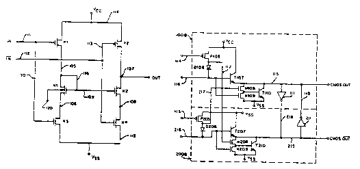
Figure 1 iilustrates the ECL-to-CMOS level translator of the present invention,
which includes p-channel fieW-effect devices P1 and P2, and n-channel devices N1-
N4. Both of the drains of devices P1 and P2 are coupled to the supply potential, Vcc,
on line 114. The ECL level input signals IN and IN/ (where IN/ is the inverse of IN) are
shown being ~uplod to the gates of devices P1 and P2 on lines 11 1 and 112,
respectively. It is appreci~ted that the input signals IN and IN/ origindLe from an ECL
or 8iCMOS logic stage; frequently an ECL or BiCMOS output buffer. Input logic
signals from the previous ECL or BiCMOS stage are generally characterized as being
equal to Vcc - Vb~ for a high logic level signal and Vcc - Vbe - VsWin9 for a low logic
level signal (where Vcc is the supp~ voltage for the ECL or BiCMOS Idgic stage, Vbe
is a typical forward biased voltage drop across a base/emitter diods junction and
Vsw;~9 is the voltage separating the high and low levels).
Input PMOS devices P1 and P2 function as input current switches. For
example, when IN is low and IN/ is high, P1 is biased on and P2 is biased at itsthreshold voltage (Vt). Note that when P2 is biased at its li,reshold, it leaks a small
drain-to-source curren~. The purposc of biasino this device ~ its threshold is to avoid
the additional time it takes to turn on an MOS transistor from a completely off state.
, y ~ / u ~ l u ~
21~1058 ~ ~PEA/US 31 AUG 1994
Because P1 is biased on, its drain to source current is significantly larger than that of
P2.
When P1 is on and P2 is at its threshold, the translator is sinking current. Thepull-down portion of the translator, comprising devices N2 and N4, is on and the pull-
up portion of the translator, comprising device P2, is biased at its threshold.
Therefore a current sinking path is established to the negative supply potential Vss
through N2 and N4. Thus the translator sinks current from the next logic stage.
The drain-to-source current of device P1 on line 105 establishes th.e input
current to the current mirror composed of devices N1 and N2. The current mirror is
configured such that the drain of N1 is coupled to its gate by line 1 16 and the ~ates
of N1 and N2 are coupled by line 109. The current of N1 is reflected to N2 on line
107 of the current mirror. Therefore, when P1 is biased at its threshold, the current
reflected through to device N2 is small. Recognize that in prior art designs, the
current flowing through device P1 is the same as the current flowing through N1.This current is re~lected to device N2 and determines the output current. The
translator of the present invention increases the output current by means of additional
devices N3 and N4.
When IN is transitioning high-to-low, two factors are affecting the voltage dropacross device N3. First, since IN is coupled to N3's gate on line 1 10, and Vss is
coupled at its source on line 115, its resistance is increasing. Second, more current is
made available to N3 due to transistor P1's simultaneous response to IN. As a result
of both of these factors, when IN transitions high-to-low, the voltage drop across N3
(voltage on node 106) is increasing. When the voltage at node 106 rises, so does the
source-to-body voltage (Vsb) of device N1. This occurs since the body of device N1 is
coupled to VS5 through line 120 and Vss remains relatively constant. Therefore, if
the voltage at node 106 increases, then the Vsb of N1 increases too. Increasing the
Vsb of device N1 raises the threshold voltage (Vt) of N1, making the node voltage at
,4M~ED SltEET
- ~WO 94/05085 2 1 ~ 8 PCr/US93/05~06
105 higher for the same drive current (the drive current being defined as the drain-to-
SOUrC8 current of P1 ) as in prior art l.;~nslalor designs. Since node -i 05 is connected
to the gate of N2, N2 is c~p~ Q of sinking more current due to its inc.easad gate-to-
source voitage (V5~s).
Also, since IN/ is coup!ed to the gats of N4 on line 1 13 and Vss is coupled to its
source on line 115, when IN is lran-~ilioning high-to-low, transistor N4's resislance is
decr~as;ny. This reduoes the ~Is~ sing voltage (on node 108) of devics N2, also
resulting in inc~ased current sini<ing capability of N2; (de~ sing occurs when the
voitage at the source of N2 ap,~roacl1es it~s gate voitage resuiting in reduced bias
voltage at it's gate). Hence the combinad effects of N3 and N4 resuits in increased
current sinking ~l~bi~ r of N2 when ECL input signal. IN, transitions high-to-iow.
In the case where IN is tranailioning low-to-high, the l-al-sidtor is sourdns
current. Device P2 is biased on and P1 is hi~se~ at its ll~r~shoid. In this condition, the
pull-up portion of the l-a,)slalor, device P2, is activated. Therefore, a portion of the
current flowing from P2 is sourced to the next loç~ic stage. In addition. a small portion
of the current flowing from P2 is flowing through N2. The reason for this is that since
P1 is biased at its threshoW, a small current flows through N1 and is reflected to N2.
Therefore, N2 is not completely off. In prior art designs this leakage current has a
deleterious effect on the current sourcing c~r~bility of the ~ sl~lor. In cOnlnaal,
devices N3 and N4 of the pr~senl invention function to reduce this leakage current,
thus inoleasillg the sourcing ~p~bility of the ~r~nslalor.
As stated above, when IN is high and IN/ low, device P1 is at its lhresl-oW and
P2 is on and sourcing current. With P1 biased at its ll,resl,oh~. only a small amount of
current is made available to N1 and N3 from P1. As a result, the volta~e drop
occurring across N3 is less. The voltage drop across N3 (seen at node 1~6) is further
decreas6d by the increase in its gate vo~tage (due to IN l-~,nsilioning low-to-high).
Increasing the gate voltage of N3 decreases its res;alance thus reducing its
, ~ w0 s4/0so8s 2 1 4 1 ~5 ~ PCr/USs3/05106
~-ssoci~ted voltage drop. Consequently, the voltage at node 106 approaches Vss. As
described above, the voltage at node 106 affects the Vt of device N1. A lower Vsb
(voltage at node 106) results in a lower Vt for N1. This l.dnslales to a smaller voltage
on node 109. Thus, the voltage at the gate of N2 is significantly lower when
compared to prior art lr~"slalor designs. This red~ction in voltage reduces leakage
current through N2 when device P2 is sourcing current. As a result, more current is
made available at the output of the ll~slalor. ~hus, the present invention provides an
increase in pull-up and pull-down drive, without increasing the drive current supplied
by P1 .
Although the current sourcing ability of the level translator of Figure 1
represents a considerable improvement over prior art translators, in most ~pp'i~tions
additional buffer stages may still be required for i"creasing the overall current drive of
a translator. Also, in some applications, it is desirable to perform a differential ECL-to-
CMOS signal translation. In the past, two separate translator/buffer stages weregenerally utili~ed to obtain a differential CMOS output. This typically involvescoupling an ECL signal and its inverse to the input of each of two level translators.
The ECL differential input signals are coupled such that one translators outputs a
CMOS signal corresponding to the non-inverted input ECL signal and the other
translator outputs the inverse of this signal. The output CMOS signal from each
translator is then coupled to a separate buffering circuit. Each of the output signals
from the two buffers comprise the t.ansldled differential CMOS signal corresponding
to the input ECL differential signal.
In cor,l,csl, the BiCMOS differential buffer of the present invention cross-
couples the inverted and non-inverted buffer stages. Figure 2 shows a block diagram
of the differential translator/buffer of the present inv2ntion. The non-invertedtranslator/buffer stage 100 comprises translator 1 00A and buffer 1008. Similarly, the
inverted translator/buffer stage 200 is comprised of trans~ator 200A and buffer 200B.
~wo 94/0so8s 2 1 ~ 1 0~ 8 Pcr/uss3/oslo6
Differential ECL input signals ECL(IN) and ECL(IN/) are coupl~d to each of ttansldlors
100A and 200A on lines 1 13 and 1 14 respectively. The ECL input signals are
co~ such that translator 1 00A outputs a CMOS signal corresponding to ECL(IN),
(output on line 116). Similarly, translator 200A O~trutS a CMOS signal corresponding
to ECL(IN/) on line 216. Thus, the signal on line 116 is the inverse of the signal on
line 216.
The translator CM~S output signals on lines 116 and 216 are couplod to
buffers 100B and 200B res~ectively. In addition, ECL input signals, ECL(IN) and
ECL(IN/) are ~ ~pled to ~uffers 1 00B and 200B on lines 1 13 and 1 14 respectively.
The signals covrl~e~ to lines 113 and 1 14 are also the inverse to each other. Buffer
100B o~r,~s a CMOS signal, CMOS(OUT), on line 115 co~-espon~ing to ECL(IN).
Buffer 200B o~ uts a CMOS signal, CMOS(OUT/), on line 215 co-.esponding to
ECL(IN/). Each of the output signals on lines 115 and 215 are the same as the
signals on 116 and 216 except that the signals on lines 115 and 215 have a greater
current drive.
When differential input signals ECL(IN) and ECL(IN/) make a lnd"silion from
one state to another, the ol~r~s of the translators follow. As an example, when
ECL(IN) goes from a high to a low ;nput level, the output of translator 1 00A (line 116)
also transitions from a high to a low CMOS level. As shown in Figure 3, the signal on
line 1 16 is coupled to buffer 1 00B. Conse~uently, the input signal to buffar 1 00B
,o~pled on line 116 makss a high to lowtransition.
Note that the output of ~ndnsldlor 200A follows the input signal ECL(IN/). SinceECL(IN/) is the inverse of sign~ ECL(IN), when ECL(IN) lndllailions from high to low,
ECL(IN/) transitions from low to high. As a result, when the signal on line 116 is
transitioning high ~o low, the signal on line 216 is ~dnsilioning in the opposile
direction.
wo 94/05085 2 1 ~ 1 ~5 8 PCI/US93/05106
As illusl~dl~d in Fi~ure 2, buffer 1 00B and. buffer 200B are cross-c~upled by
lines 1 17, 217, 1 18, and 218. The purpose of cross-coupling lines 1 17 and 217 is to
speed up the pull-down portions of buffers 100B and 200B. Lines 1 18 and 218
provide a feedback technique which functions to drive output signals to Vcc and Vss~
Note that trans~ators 1 00A and 200A of Figure 2 may either comprise the level
translator of Figure 1, or a conventional translator. Howevsr, if conventional
translators are utilized, then an additional CMOS inverter stage may be necess~ydepending on the current drive requirements of the next logic stage.
Figure 3 shows a schematic diagram of one embodiment of the cross~ouple~
differential buffers 1 00B and 200B of the present invention. There are four basic
elements in each of buffers 1 00B and 200B: 1 ) an emitter follower which incr~ases
the pull-up current drive of an input signal; 2~ a bipolar transistor configured as a
diode for providing a bias potential equal to a Vbe for the pull-down driver; 3) a pull-
down bipolar driver to improve the pull-down drive; and 4) output level circuitry for
driving output levels to vcc and Vss
The emitter followers of buffers 1 00B and 200B include transistors T107 and
T207, respectively. Bipolar transistors are utilized to take advantage of theircurrent
drive ~r~hilities when compared to MOS devices. Driver transistors T107 and T2~7are turned on or off by input signals 116 and 216, respectively. Since signals 116 and
216 are the invers2 of each other, only one of transislors T107 or T207 wiîl be turned
on at a time; the other will be off. For example, when the voltage on eithar of lines 116
or 216 is greater than a Vbe, one of transistors T107 or T207 is turned on and sources
current to the next logic sta~e. As a result, a high output level is seen on the output of
the buffer in which the driving transistor is turned on. On the other hand, when the
voltage on either of lines 1 t 6 or 216 is less than a Vbe, one of transistors T107 or
T207 is off, causing either of buffers 1 00B or 200B to sink current. As a result, a low
~wo s4/osos~ 2 1 4 1 05 ~ PCr/USg3/05106
14
output voltage level is seen on the output of the buffer in which the driving l-dns;slor is
turned off.
The Vbe bias source for each of buffars 100B and 200B is comprised of P105
and T106 which is configured to function as a diode (buffer 100B~ and P206 and T206
which is also confi~ured to function as a diode (buffer 200B). PMOS d~vices, P105
and P205, provide a small trickle current to ,.-ainLai,- the Vbe bias voita~e when lines
116 or 216 are driven io~. P105 and P205 aiso drive the anode of diodes T106 andT206 to Vcc, respectively, when their gates are driven low. For exs.nple, when the
gate of P10~ is low, the anode of diode T106 approaches Vcc. At the same time, the
signal on the cathode of diode T106 is transitioning from a low-to-high voltage level.
Diode T106 will be forward biased when the voltage on its call.ode is at least equal to
a Vbe lower than the voltage on its anode. Ther~for~, sincs the anode of diode T106
is courlsd to approximately Vcc, and its cd~ Je is t-dnsilioning low-to-high, T106 will
be on untii its ~Ihode voltage llansilions to a voltage close to Vc As long as T106 is
on, the voltage on signal line 117 is equal to a Vbe above the voltage on line 116.
Note, sincs the signals on line 114 is the inverse of the signal one line 113 only one of
the PMOS transislor~ will be on at a time and thus, only one diode will be functioning
as a bias source at one time.
The pull-down p~s.tion is ano~l-er funda---e,)tal ele~ellt in the differential buffer
of the present invention. This pull~own circLJitry is capable of dischargi-,s relatively
large capaali.~e loads while i-"posin~ a relatively low load to its driver when
compared to conventional CMOS drivsrs. The pull-down portion of buffer 100B
co""..ises devicss N108, N109 and T110. Similarly, the pull-down portion of buffer
200B comprises devices N208, N209, and T210. Since the differ~ntial cross~oupledbuffers of the present invention operale such that oile buffer sources currant while ~he
other sinks current, only one pull-down portion will be on at a time. Ths pull-down
portion of buffer 100B operates such that when devicss N109 and T110 are active, a
WO 94/05085 PCr/US93/05106
2 1 ~ 8
current path is est~hiished between output line 115 and Vss. Therefore, bufler 100B
can sink current through N108 and T110 to Vss thereby causing output line 11~ totransition from a high-to-low state. Similarly, when devices N209 and T210 are active;
buffer 200B sinks current, and output 21~ may transition from a high-to-low state.
As can be seen in Figure 3, to es~ h the current sinking path in one of the
pull-down portions it is necess:~ry to provide enough voltage to overcome the
esllold voltage (Vt) of either ~1108 or N208 and the base-to~mitter voltage (Vb~) of
either T110 or T210. Thus, one of the pull-down portions of buffers 1 OOB or 200B are
on if the voltage on the gates of N108 or N208 is greaterthan a voltage equal to a Vt
plus a Vbe-
To deactivate the current sinking portion of the pull-down circuitry, it is
necess~ry to turn on either N109 or N20s. This is acoomplished by applying a
voltage greater than a Vt on the gates of either N109 or N209. By turning either N109
or N209 on, the base of either T110 or T210 will be discharged; thus ensunng that the
current sinking portion of the pull-down circuitry is off.
The high-to-low transition time of the output signals on lines 1 15 and 21~ are
dependent on how quickly the pull-down portion can dnve lines 11~ or 215 to Vss.Therefore, the quicker the pull-down portions are activated, the faster the high-to-low
transition times will be. Commonly, in prior art buffer designs, the voltage signal that
is coupled to and controls the pull-down circuitry is the inverse of the input signal that
is co~pled to the driving transistor. Consequently, the inverse of the input signal to the
driver transistors, T107 and T207, determines how quickly the pull-down portion of the
buffer is activated. But the input signal to the driver L,~nsi-~lon are taken from the
output of the preceding translator stage. Thus, it follows that the translator output
signal determines how quickly the pull-down portion of each buffer is activated.In the present invention, however, the voltage signal coupled to the pull-down
portion of the present invention does not come from the output of the preceding
WO 94/05085 2 1 ~ 1 05 8 PCr/US93/05106
16
translator stage. Instead, the voltage signal coupled to the pull-down portion of one
buffer stage is cross-coupled from another preceding translator output through adiode. Flgure 3 shows that for buffer 1008, the gate of pull-down devic~ N108 (the
input device for the pull-down circultry) is coupled to the anode of diode T206 by line
217. The cathode of T206 is cour~lQd to line 216 (the output signal of translator 200A).
The purpose of the bias diode design is to cause one of the pull-down portions of the
differential buffer to tum on sooner than if it were simply OUplQC~ to the output of the
preceding translator stage. For example, when the voltage on line 113 is low, device
i205 is on. As a result, the anode of diode T206 is couplQd to Vcc and is also on.
T206 remains on as long as the voltage on line 216 is low enough to keep T206
forward bia3e 1 Consequently, T206 acts as a bias sourcs approximately equal to a
Vb~. Therefore, the voltage ~pp'ied to the gate of N108 is equal to one Vb~ higher
than the voltage on line 216. Hence, the voltage neces~ry to tum on devices N108and T110 is achieved sooner than if just applied straight from the previous translator
stage.
Figures 4A shows the voltage signal seen by the gate of N108 when biased at
a Vb~ similar to the configuration of the present invention. Line 301 represents the
inverse of the volta~e signal s~pplied by the output of the preceding l-a-)sldlor output
(line 116 of Figure 3). In prior art designs this signal is couple~ to the gate of input
pull-down device N108. As can be seen in Figure 4A, voltage signal 301 reaches the
turn-on voltage (Vt + Vbe) of the pull-down circuitry at a time of T1. Therefore at time
T1, the pull-down circuitry is activated and starts sinking current. As a result, the
output voltage of buffer 100B (voltage signal on line 115) begins to lldnSiliOn from a
high-to-low level. Figure 4C illustrates the output voltage on line 115. Une 306shows the output signal transitioning high-to-low at a time T1 (the time when th~ pull-
down circuitry is activated). This occurs when the inverse of signal 116 reaches a
voltage equal to (Vt + Vbe)-
' ~o 94/0508~ 2 1 4 1 ~ 5 8 PCT~US93/05106
Figure 4B illustrates the voltage signal seen by the gate of N108 when biasedat a VVbe similar to the configuration of the present invention. Un~ 302 is the voltage
signal on line 216 (Figure 3). As can be seen when comparing Figur~s 4A and 4B,
the inverse of the voltage signal on line 116 is essentially the same as the signal on
line 216. As described above, the voltage signal col)rle~ to the gate of N108 (on line
217) is at a potential equal to one diodl3 drop above the signal on line 216 when
configured as ~isclose~J by the present invention. The relationship between the
voltage signals coup!ed on 217 and 216 is illustrated in Figure 4B. Line 303 (voltage
signal on line 217) is approximately one diode drop above line 302 (voltage signal on
line 216). Therefore, the signal on line 217 reaches the turn-on voltage (Vt + Vbe) of
the pull-down circl ~itry at a time T2. Therefore at a time T2, the pull-down circuitry is
activated and starts sinking current. Figure 4C (line 307) shows the output signal on
lina 11~ transitioning high-to-low at a time T2. As can be seen in Figure 4C, a high-to-
low output transition on line 11~ Figure 3 (signal 307, Figure 4C) occurs sooner than
the output signal 306 (Figure 4C). Therefore, high-to-low output transitions times are
improved when utilizing the present invention cross~ouplod buffer design. Thoughthe differentail buffer of the present invention is described in conjunction with the level
translator of the present invention, it can be utilized with any BiCMOS logic stage that
requires differential buffering.
Another element commonly found in buffering stages is a differential CMOS
output level driver. The driver ~unctions to drive the difFerential o~plJts to the high and
low CMOS output levels. The reason this is needed is because differential buffers
100B and 200B can only drive nodes 115 and 215 to a voltage that is either a Vbefrom Vcc or Vss, i.e. a Vbe from the desired CMOS high and low level voltages. For
example, when buffer 1 00B is transitioning high-to-low, the voltage on the collector of
T1 10 (which is the same as the output voltage signal on 115) will be approaching
ground. However, when the voltage on the coliector reaches Vbe, it becomes biased
,
~WO 94/05085 PCI/US93~05106
21hlO58
18
such that it tums off. Ther~ror~, the pull~own circ~itry can only pull the output signal
on line 11 S to a vottage equal to approximately a Vbe above Vss. Similarly if buffer
200B is t,~nsilioning from a low-to-high level, T207 is biased on until the output signal
on line 215 r~a~l.es a voltage of Vcc - Vb~. Differential buffer output siy"als that are
not truly at CMOS high or low level vqlt~es may lead to an accumulated amount ofleakage ourrent resulting in i"c.eased power~ slr~;on in s~ se~luent lo~ic stages.
Consernently, an inverter configuration such as.shown in Fi~ure 6A is cG",.oonlyutilized to drive output nodes 116 and 215 to either high or low CMOS output levels.
The prior art inverter configuration shown in Figure 6A is c~ ,,ised of two inverters
per output for a differential buffer (a total of four per one diiffer~"li~l output buffer~. As
shown, the CMOS(OUT) output line 115 of ~ e,t",lial buffer ~iOOB is coupled to the
input of inve ter 500 and the output of inverter ~01. The output of inverter 500 and the
input of inverter 601 are also oour'e~ together. CorrespG"~-ir~ly, the CMOS(OUT/)
output line 216 of differential buffer 200B is co urle~ to the input of inverter 502 and
the output of inverter 503. The output of inverter 602 and the input of inverter 603 are
also col~pleri to~etl.er. Since the inverters have an input trip level of VC~/2, the
inverter configurations function such that if an output signal seen on either of lines 11
or 215 are not at CMOS high and low voltage level (Vcc or Vss), the inverters drive
the signal to either Vcc or Vss. One main disadv;3nlaye of this type of inverterscheme is the number of inverters neces.s~ y to ac~l~lno~iale a differential output.
When spac~ cons~ ation is an issue, this prior art inverter desi~n may be
aJmbersome. Another co"- l-dint of the prior art invener design is that it adds the
power ~;S~S;PA1;OI~ of four inverters. Therefore, in memory ~ie~;~ans in which space and
power consumption are extremely i,--~x~,lant f~ors, tha prior art inverter design can
present some limitations.
The present invention ~tiii~es a cross~oupled invarter design as shown in
Figure 3. As nl~ ldle~, output line 115 is coupleci to the input of inverter 111 the
~WO 94/05085 2 1 ~ 1 05 8 PCI/US93/05106
19
output of inverter 111 being coupled to output linç 215. Similarly, output line 215 is
coupled to the input of inverter 211 the output of inverter 211 being coupled to output
line 115. In companson to prior art inverter designs, only two inverters are necess~ry
for a differential output. Therefore, the present invention inverter design reduces the
number of inverters necess~ry by 50%. The inverter design of the present invention
consumes less powsr than prior art designs since only two inverters are necess~ry to
drive each of the differentiai outp~ ~tc to the CMOS high or low voltage levels.The level driver shown in figure 3 functions such that if the output signal on line
21~ is transitioning from a low-to-high voitage and reaches the VCC/2 trip pointvoltage of inverter 211, it r~useS the output of inverter 211 to drive output lins 115 to a
CMOS low level voltage, i.e. Vss. The output of inverter 21 1 (output signal 115)
feeds back to the input of inverter 1 1 1. Thus, the output signal on line 215 is driven to
a high CMOS level (Vcc).
Although the elements of the present invention has been described in a
conjunc~ion with certain embodiments, it is appreci~ted that the invention may be
implemented in a variety of other ways. By way of example, the differential buffering
stage may be coupled to any differential logic stage. Or, the translator of the present
invention may be coupied with other buffering stages. Consequently, it is to be
understood that the particular embodiments shown and deso,ibed by way of illustration
are in no way intended to be considered limiting. Reference to the details of these
embodiments is not intended to limit the scope of the claims which ll,e",selves recite
only those features regarded as essential to the invention.
Thus, the present invention offers an improved BiCMOS ECL-to-CMOS level
tranclator and BiCMOS buffer.