Note : Les descriptions sont présentées dans la langue officielle dans laquelle elles ont été soumises.
Certificate of ''Express Mail" Filing
No.: IB434025856US
Date of Dep~sit: January 28, 1994
I hereby certify that the enclosed patent
7840 application and filing fee are being deposited
with the United States ~ostal Service "Express
Mail Post Office to Addressee" service under
37 CFR 1.10 onthe date indicated above ~nd is
addressed to the Commissioner of Patent~ and
Trademarks, Washington, DC 2023~ . ~ /
/J~h~ S. Vale
Regi ~ ation No. 25,937
Title: ELECTRONIC IMAGING MODULE
BACKGROUND OF THE INVENTION
1. Field of the Invention
The present invention relates generally to conventional photographic cameras
and more particularly to an electronic imaging module that is removably insertable
therein for reversibly converting such a conventional camera into an electronic
imaging camera.
5 2. Description of the Prior Art
In conventional photographic cameras, image recording typically is performed
by sequentially projecting optical images of subjects onto a roll of film formed from
a silver halide based emulsion. Photons strike chemical grains in the silver halide
emulsion and form a latent images that are stored in the emulsion. After completing
10 exposure of all the frames on the roll of film, the latent images are developed by
chemical processing and are viewed directly or printed on positive paper.
While conventional photographic camera and film systems do produce high
resolution, continuous tone photographs at modest cost, such systems do have
certain limitations. For example, image storage and retrieval is inconvenient and time
15 consuming, and it is difficult and costly to copy, modify or transmit photographic
images. Also, to use such images in electronic computer or video systems, the
photographic image must first be converted to an electronic image in the form of an
electrical signal which is representative of the photographic image.
2141386
To overcome these limitations, carneras have been implemented with
special electronic means such as a charge-coupled device (CCD) for recording
images electronically and a storage device such as a tape, disk or a memory circuit
for storing electrical image signals. The image signals are l.ansrer,ed to a display
5 device like a CRT for direct viewing or a printer for printing. The advantages are that
the electronic images can be easily modified in format, resolution, color mapping, and
special optical effects can be added. Also, the images may be easily transmitted to
remote locations.
Electronic imaging systems incorporating the foregoing features are well
10known. For example, United States Patent Number 4,916,476, issued to McGarvey,discloses an electro-optical circuit for converting a conventional single lens reflex
(SLR) camera into an electro-optical camera. The electro-optical circuit is attached
to the film back of the camera so that it is operational as a still camera or as an
electro-optical camera.
15United States Patent Numbers 4,953,029 issued to Morimoto et al. and
4,814,811 issued to Saito et al. disclose still camera systems that are capable of
being loaded with film backs or still video backs 2 for forming an image and
transferring it onto a magnetic media.
United States Patent Number 4,862,293 issued to Saito et al. discloses a still
20 video adapter attached to a still video back at the rear cover of a SLR camera body.
The still video adapter includes a CCD for receiving an image of an object
photographed, a signal processing circuit for processing and transferring the image
data to a magnetic disk attached to the side of the camera.
Another electronic still camera system using an adapter is shown by Holland
25 in Electronic Photographv and the NASA Experience. In this system, there is shown
a removable hard drive attached to the side of a Nikon F4 camera via an adapter.Images are recorded on the hard drive and sent to a control station for viewing and
printing.
United States Patent Number 5,150,215 issued to Shi, discloses a camera
30 system having film and still video functions. This camera operates in three modes.
In the first mode, the camera is in a still video image mode only. In the secondmode, the camera is in the photo film mode only. In the third mode, the camera is
in the still video image mode and the film photo mode simultaneously.
2141386
SUMMARY OF THE INVENTION
The above electronic imaging systems are expensive and require special
attachments to the cameras such as interchangeable film backs and adapters. Boththe interchangeable film back and the adapter are bulk~ and occupy a substantial5 arnount of room in the camera. Furthermore, the film back and the adapter are not
very practical to the average camera user. Most carnera users are familiar with the
operation of conventional cameras, but are hesitant to spend the time and efforttrying to learn how to use these cumbersome film backs or adapters.
Therefore, it is a primary object of the present invention to provide an
10 electronic imaging module that is capable of being easily rel(orilled into a variety of
conventional photographic cameras without having to use intercl langeable film backs
or special adapters.
Another object of the present invention is to provide an electronic imaging
module that is removably insertable in the conventional camera at its film cassette
15 holder location. This feature gives the user the options of using conventional silver
halide film with the camera or reversibly converting the camera into an electronic
imaging camera.
Still another object of the present invention is to provide an electronic imaging
module that is capable of communicating with a remote control unit and a base unit
20 for immediate image viewing and printing.
Yet another object of the present invention is to provide a method employing
an electronic imaging module for reversibly converting a conventional photographic
camera into an electronic imaging camera.
Thus, in accordance with the present invention, there is disclosed an electronic25 imaging module that is removably insertable in a conventional camera wherein at
least a portion of the electronic imaging module occupies the camera's film supply
or cassette holding location.
The electronic imaging module includes means for sensing an object image
in accordance with the camera film format and converting the object image into an
30 electrical signal corresponding to the object image. A processing means processes
the electrical signal into a format suitable for transmission. A coupling means
couples the sensing means to the processing means. The coupling means is
2141386
adjustable to align the sensing means with the camera optical path and film plane
and maintain the processing means within the carnera film c~s~tle holder location.
In a second embodiment of the present invention, the electrical signal in the
processing means is transmitted immediately to an external control unit by a wireless
transmitting means. The co"l,ol unit receives the electrical signal at a wireless
communication means. The control unit has a command panel for controlling the
resolution, storage, display, and transmission of the electrical signal. Also, included
is a display for viewing the images.
In a third embodiment of the present invention, the electricaJ signal is stored
in the processing means at a storage means. After all the frames on the electronic
imaging module have been taken, the module is removed from the carnera and
inserted into a base unit. A wired transmission means transmits the electrical signal
to the base unit at a communication means. The base unit includes a processing
means for processing the electrical signal, a storage means for storing the electrical
signal, a display for displaying electrical signal as an object image and a printer for
printing the object image.
In a fourth embodiment of the present invention, the electronic imaging
module, the control unit, and the base unit are used in cooperation. In this
embodiment, the processing means simultaneously stores the electrical signal in the
storage means and transmits the electrical signal to the external control unit. The
electrical signal stored in the storage means is retrieved later by inserting the module
in the base unit. On the other hand, the object image received at the control unit is
viewed immediately. A link is provided, so that the user can transmit the image from
the control unit to the base unit for initiating storage or printing.
Embodiments of the present invention are disclosed for use in connection with
photographic cameras that use conventional film and cameras that use "self-
developing" film.
While the present invention will hereinafter be described in connection with
several preferred embodiments and methods of use, it will be understood that it is not
intended to limit the invention to these embodiments and methods. On the contrary,
it is intended to cover all alternatives, modifications and equivalents as may be
included within the spirit and scope of the invention as defined by the appendedclaims.
` 2141386``
-
BRIEF DESCRIPTION OF THE DRAWINGS
Figure 1A is a schematic cross-sectional view of a conventional 35mm
photographic camera having one embodiment of an electronic imaging module of thepresent invention therein.
Figure 1 B is a perspective view of the e~ectronic imaging module of Figure 1 A.Figure 2A is a schematic cross-sectionaJ view of a conventional 35mm
photographic camera having another embodiment of an electronic imaging module
of the present invention therein.
Figure 2B is a perspective view of the electronic imaging module of Figure 2A.
Figures 3A-3B are diagrammatic perspective views of an electronic imaging
module of the present invention.
Figures 4A-4B are block diagrams showing the electrical functions of the
electronic imaging module.
Figure 5 is a cross-sectional view of the electronic imaging module of Figure
1A.
Figure 6 is a schematic representation of the electronic imaging module
interacting with an external control unit.
Figure 7 is a block diagram showing the electrical functions of the electronic
imaging module and the control unit.
Figure 8 is a schematic representation of the electronic imaging module
interacting with a base unit.
Figure 9 is a block diagram showing the electrical functions of the electronic
imaging module and the base unit.
Figure 10 is a schematic representation of the electronic imaging module
interacting with the control unit and the base unit.
Figure 11 is a block diagram showing the electrical functions of the electronic
imaging module, the control unit, and the base unit.
Figure 12 is a schematic representation of the electronic imaging module and
the control unit interacting with PCMCIA card.
Figures 13a-13b are block diagrams showing the electronic imaging module
having a communication channel with the carnera.
Figure 14 is a perspective view of a self developing camera and an electronic
imaging module configured for use therewith shown in its folded position.
2141386
Figure 15 is a side elevation view of the electronic imaging module of Figure
14 shown in its erected position .
Figure 16 is top planar view of the electronic imaging module of Figure 15.
DETAILED DESCRIPTION OF THE INVENTION
The electronic imaging modules of the present invention are disclosed as
being embodied pre~erably for use in conventional photographic cameras which useconventional or "self-developing" film. Bec~se the features of such conventionalcameras are generally known, the description which follows is directed in particular
only to those camera elements cooperating directly with the disclosed electronicimaging modules. It is to be understood, however, that other camera elements maytake various forms known to a person of ordinary skill in the art.
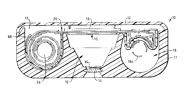
Referring to the drawings, Figures 1 A and 2A show a schematic cross-sectional
view of a conventional 35mm photographic camera 10 with which electronic imagingmodules incorporating the features of the present invention are adapted to be used.
The illustrated camera 10 is of the direct viewing, automatic, "point and shoot" type
and includes a main housing section 11 and a hinged rear door 12 providing access
to the interior of the camera. Within the housing section 11 is a central cone shaped
exposure chamber 13 having an objective lens 14 at the forward end for forming afocused image of a subject (object image) at an aligned film exposure or focal plane
15 at the rear of exposure chamber 13. Just behind lens 14 is a shutter 16 for
controlling the transmission of image forming light from lens 14 to exposure plane 15.
Disposed laterally on opposite sides of exposure chamber 13 is a film supply
chamber 17 for removably receiving a standard 35mm film cassette (not shown)
holding a roll of conventional, silver halide photographic film therein; and a film take-
up reel chamber 18 having a film take-up reel 1 8a therein onto which the exposed
portion of the film roll is wound for storage until all frames of the film have been
exposed. At the rear of exposure chamber 13 is a pressure plate 19, which is spring
mounted on the interior of rear door 12, for urging that portion of the film extending
across the rear opening of exposure chamber 13 into its proper position at the film
exposure plane 15.
2l4l386
One aspect to the present invention is to provide means, in the form of an
electronic imaging module, that is adapted to be easily and removably inserted into
a conventional photographic camera, for example the illustrated camera 10, f~r
reversibly converting such a camera into an electronic imaging camera. As will
5- become apparent, such a module is designed to be easily inserted and removed
without the need for special tools or skills. The use of such an electronic imaging
module does not in anyway impair the carnera's capability to function again as aconventional photographic camera once the module has been removed.
One such electronic imaging module 20 embodying the present invention is
shown in perspective in Figure 1 B and at its operative position within camera 10 in
Figure 1A.
The object image formed by lens 14 is sensed by a later to be described
central sensor unit 22 of module 20 located at the film exposure plane 15 of camera
10. One end unit 24 of the electronic imaging module 20 is removably inserted and
received in camera 10 at its film cassette holder location within film supply chamber
17. In this illustrated embodiment, the electronic imaging module 20 includes anoptional opposite end unit 27 which is removably inserted and received in take-up
reel chamber 18. The central sensor unit 22 of electronic imaging module 20 is
urged into it operative position at exposure plane 15 by pressure plate 19 located on
the inside of rear door 12. In this particular module 20, the object image formed by
the lens 14 is detected by the sensor unit 22 which produces an electrical signal
representative of the image. Module 20 processes this signal for either storage within
the module 20 or transmission to later to be described remote means for immediate
viewing or printing.
Views of the electronic imaging module 20 are shown in further detail in
Figures 1A,1 B, 3A-3B and 5. The illustrated electronic imaging module 20 is shown
as having the central sensing unit 22, a processing unit 24 at one end, a coupling
unit 26 coupling sensing unit 22 to processing unit 24, an optional component
housing unit 27 at the opposite end, and its associated coupling unit 27a for
physically coupling unit 27 to sensing unit 22. As will become apparent later,
electronic components in housing unit 27 may be electrica~ly connected to
components in sensing unit 22 and/or processing unit 24. The sensing unit 22
~ 2191386
includes a sensor with support circuitry 28 centrally mounted on a flat base plate 29
which has a peripheral, fonNardly projecting, rectangular, locating frame or ribstructure 29a that is dimensioned to closely fit into ~e rear opening of exposure
chamber 13 and thus accurately locate the sensor 28 with respect to the optic axis
of lens 14. Portions of base plate 29 outboard of frame 29a engage the back end of
the exposure chamber defining wall to accurately locate sensor 28 at the exposure
or film plane 15.
With reference to Figures 3A and 3B, the processing unit 24 includes a
microprocessor 30 typically with either a wireless transmission link 32 (Figure 3A) or
an image storage unit 33 with a wired transmission link (Figure 3B). However, it is
within the scope of the present invention to provide a processing unit 24 that includes
both a wireless transmission link 32 and a storage unit 33.
As used herein, the term "wired" means that an electronic device, such as
storage unit 33, is configured to receive and or transmit electrical signals over an
electrically conductive wire, cable, data bus, or the like connected thereto.
Processing unit 24 may include a battery 34 for powering the various electronic
components of module 20, or the battery 34 (and/or other module components)
optionally may be housed in optional component unit 27. While the diagrammatically
illustrated battery 34 is cylindrical, it may be configured as a thin flat or curved battery
to more readily conform to the contours of optional component housing 27.
The coupling unit 26, and optional coupling unit 27a if unit 27 is used, are
flexible connectors which, respectively, mechanically and electrically couple the
sensing unit 22 to the processing unit 24, and couple component housing unit 27 to
sensing unit 22 and/or processing unit 24. The reason the coupling units 26 and 27a
are made flexible is to provide a some amount of width adjustment in the electronic
imaging module 20 to accommodate a wide variety of 35mm cameras. Alternatively,
the coupling units 26 and 27a may be formed as telescoping sliders to provide such
width adjustment.
In 35mm cameras that are designed to accept standard 35mm film cassettes,
it has been found that: there are not specified standard lateral dimensions for the
distance between the optic axis of lens 14 and the central axis of a 35mm film
cassette located in supply chamber 17 or the distance from the lens axis and the axis
2I41386
of take-up spool 18a; and these dimensions vary somewhat in di~ere~l cameras.
Thus, by providing flexible coupling units 26 and 27a (if used) in electronic imaging
module 20, the lateral spacing of the major module components may be adjusted toaccommodate a wide variety of 35mm cameras. Accordingly, when the electronic
imaging module 20 is inserted into the camera 10, the processing unit 24 can be
positioned in the film cassetle holder location in film supply receiving chamber 17 and
the sensing unit 22 can be held in alignment with the camera's optic axis and the
focal plane. Also, if optional component housing unit 27 is used, it may be easily
aligned with the take-up reel 18a.
Flexible couplings 26 and 27a may be made of any of the well known fiex
circuit materials which typically have electronic components connected to thin flexible
copper conductors bonded to a thin, flexible, plastic, insulating base material such
as Kapton(~, Mylar(g or the like. One such conductor 26a of coupling 26 is shownin Figures 1 B and 2B in a section that has been cut away for illustrative purposes.
It has also been found that while there is no standard specified dimensions for
the rear opening of the exposure chamber 13 adjacent the film exposure plane 15,there is very little variation in the size of this opening in a wide variety of 35mm
cameras. Thus, a fixed sized locating frame or rib structure 29a on sensing unit 22
will serve to accurately align unit 22 with respect to the objective lens optic axis and
the film exposure plane. Alternatively, the ribs forming frame 29a may be mounted
on base plate 29 so that their positions may be varied to make the size of the
locating frame 29a adjustable to fit an even larger variety of 35mm cameras.
Figure 5 shows electronic imaging module 20, including the optional
component housing 27, in cross-section. The processing unit 24 comprises a hollow
housing 35, having the general shape and size of a 35mm film cassette, in which is
stored a stack of electrically interconnected circuit boards 36 have various electrical
components and subsystems 37 of the micro processor 30, storage unit 32 or
wireless link 33 thereon. Such components and subsystems that need to be
connected to the sensor unit 22 are so connected by the coupling unit 26. Unit 27
comprises a hollow housing 38 that is dimensioned to fit into the camera take-upspool chamber 18 and includes a concave bottom wall section that conforms to andprovides clearance for the take up spool 18a. Inside is a circuit board 36 having
2141386
components mounted thereon that electrically connected to sensor unit 22 and/or
processing units via coupling units 27 and 26. In this illustration, the components are
a plurality of small batteries 34 for powering module 20. Alternatively, a single battery
34, may be provided in housing 38.
As an alternative to using rigid circuit boards 36 in the processing unit 24 andoptional housing 27, various components 37 may be mounted on flex circuit as
shown in Figures 1A and 2A. In this embodiment, that portion of flex circuit in the
processing unit 24 is formed into a roll with room left in the center for a battery 34.
The portion of the flex circuit in housing 27 may be curved and folded to conform to
the interior shape thereof.
The sensing unit 22 and processing unit 24 of the electronic imaging module
20 are shown diagrammatically in further detail in Figures 4A-4B. The sensor andsupport circuitry 28 includes an image sensor 40 for sensing an object image andconverting the object image into an electrical signal. Image driver circuits 42,regulated by corresponding image driver regulators 43, connected to the image
sensor 40 drive the sensor to acquire image data and convert it into a corresponding
electrical signal that is representative of the image. The electrical signal generated
from the image sensor 40 is sent to a video signal processor 44 via an emitter
follower 46. The video signal processor 44 samples and conditions the electricalsignal to extract relevant information. The video signal processor 44 of the present
invention includes a preamplifier for amplifying the electrical signal. The electrical
signal is sampled and held in a sample/hold circuit. After the electrical signals are
conditioned, the video signal processor 44 outputs the image information to the
processing unit 24.
In the processing unit 24, the electrical signal sent from the video signal
processor 44 is received by an analog-to-digital (A/D) converter 48. The A/D
converter 48 takes the analog electrical signal and splits it into discrete samples. The
discrete samples are then digitized. Figure 4A shows the A/D converter outputting
the digitized signal to the microprocessor 30 and the image storage unit 33, which
is non-volatile, solid-state, and has a large storage capacity. In the present invention,
the image storage unit could be a SRAM, PSRAM, PROM, EEPROM, or the like. The
digitized image signal is then transferred to a later to be described external base unit
through a wired transmission link 50.
21~1386
..
Figure 4B shows the AID converter 48 outputting the digitized signal to a later
to be described external co, Ill ol unit through the wire~ess ll ~ ,smission link 32. Before
transmission, the digitized signal is sent to a frame buffer 52. The frame buffer 52 is
required if the data l,ansr"ission rate of link 32 is less than the image sensor readout
5 rate. In the event the transmission rate of link 32 is higher, the frame buffer is not
required. A digital signal processor (not shown) could be insel l~ in Figures 4A and
4B and connected to the A/D converter for enabling further image processing.
The timing and operation of both embodiments are controlled by the
microprocessor 30. The timing and operation of the microprocessor 30 is set by a10 programmable array logic circuit 54 and an oscillator 56. The timing and operation
commands generated from the microprocessor 30 for the sensing unit 28 are sent via
a digital-to-analog converter 60 to video signal processor 44.
In the present invention, the image sensor 40 is preferably a CCD. The CCD
is an image array formed from a plurality of photosensitive elements arranged in a
15 matrix of rows and columns having respective electrodes connected in common.
Incident light is stored as a charge in one electrode during integration. To read the
signal, the charge is shifted to a second electrode, where it induces a voltage
change. The voltage change is detected by a sense amplifier connected to the
second electrode. The voltage change is transferred out of the CCD as an analog
20 voltage. The CCD is then cleared and prepared to acquire more image information.
Although the CCD is preferred, other sensors such as a charged injection device
(CID), a stitch sensor, a subframe sensor, or a full frame sensor are within the scope
of the present invention.
Regardless of which sensor is used, it is important that the sensor format
25 match the film format of the camera. Matching the sensor format to a 35mm film is
not a problem if the sensor has a one-to-one correspondence with the frame size of
the film. However, since the frame size of 35mm film is approximately 24x36mm, at
the present time it may not be desirable from an economic standpoint to use a single
CCD of that size. In fact, a typical commercially available CCD is about 1/4 of the
30 35mm frame size. Thus, to use a CCD of this size it is necessary to demagnify the
image so that the image format matches the sensor format.
2141386
-
There are several approaches to demagnifying the image so that there is a
match between the sensor format and the image format. One approach of
demagnifying the image is by designing a special objective lens to the reduce the
image size. In a SLR camera, it is possible to attach a demagnifying lens in front of
5 the camera, since this type of camera has interchangeable lenses. Another way to
demagnify the image is to provide an auxiliary lens or lens assembly in the electronic
imaging module optical path to reduce the image size as will described later with
rererence to such an embodiment shown in Figures 2A and 2B, and a second such
embodiment in shown in Figures 14-16. A third approach of demagnifying an image
is by using a fiber optic bundle to refocus the image to a flat plane instead of the
usual curved surface. A flat plane results in smaller image than in a conventional
curved plane. A fourth approach of matching the image to the sensor format is bydesigning a sensor for a large film format.
A large format sensor may be provided by fabricating an image array on a
substrate separate from a readout array (i.e. amplifiers, shift registers, etc.). After
fabrication, the imaging array is then bonded to the substrate using flip-chip
technology, or equivalent means that use a contact on the end of each electrode. The
contact connects to a trace on the substrate, which then leads to another contact that
is connected to the readout array mounted on the same substrate. ~Ith this
approach, the hybrid integration of the image array and the readout array enables
optical matching with larger film formats in a cost effective manner. Additionally, the
fabrication technology can be selected independently for the image array and thereadout array, and consequently optimized for that particular functionality.
Matching the sensor to the film format of a 110 camera is much easier than in
the 35mm camera because the 1 10 frame size 1 3x1 7mm is much closer to the sizeof reasonable priced CCDs that are commercially available at this time.
As noted earlier, the electronic imaging module of the present invention may
be embodied to include built-in image demagnifying optics allowing the use of a CCD
sensor that than is smaller than the frame size of the camera film format. With
reference to Figures 2A and 2B, another embodiment of an electronic imaging
module, designated 20b therein, is shown configured for use in the same 35mm
camera 10, but includes a centrally disposed, forwardly projecting housing section
2141386
62 mounted on the base plate 29. Housing 62 has angled walls bhat are sized and
shaped so that housing 62 conforms to and fits into the camera's exposure chamber
13 when the module 20b is located at its operative position in Camera 10 shown in
Figure 2A,
At the forward end of housing 62 is an auxiliary demagnifying lens assembly
64 which is aligned and cooperates with camera objective lens 14 to provide a
focused object image that is smaller than the image produced by lens 14 alone at a
focal plane 65 that is located forwardly of the camera's normal focal plane 15 at the
rear of exposure chamber 13. This embodiment permits the use of a smaller, and less
costly, sensor and support circuitry 28b which is mounted in housing 62 behind lens
assembly 64 with sensor 40b at the closer focal plane 65. By proper design of lens
assembly 64, the image may be reduced to any appropriate smaller frame size (e.g.
12x18mm) that is compatible with less expensive commercially available CCDs.
Operation of the electronic imaging module 20 (or 20b) is initiated by insertingthe module in the camera 10 at its position shown in Figures 1 A or 2A as the case
may be.
To avoid confusion, in the following description of the operation of the
electronic imaging module, reference will be made to module 20 only with the
understanding that the description applies equally to the modified module 20b unless
it is noted otherwise.
The electronic imaging module 20 is inserted so that the sensing means 22 is
in alignment with the camera optical path and film plane and the processing unit 24
is located within the film cassette holding location or receiving chamber 17. The
adjustable coupling means 26 ensures that the sensing unit 22 and the processingunit 24 fit in many types of cameras. If optional component housing unit 27 is used,
it fits into take-up reel chamber 18 with adjustable coupling 27a ensuring proper fit.
The electronic imaging module 20 may optionally include indicia, such as the
illustrated stripe(s) or band (s) 68 on the outside of the processing unit 24,
representative of an ISO rating for cameras that have the capability of sensing DX
formatted film. In the illustrated camera 10 there is contact 69 (only one shown) such
film speed indicia.
2141386
Once the electronic imaging module 20 has been inserted in the camera, the
module is ready to acquire images. However, before data acquisition can occur, the
module has to determine whether the camera 10 is ready to initiate acquisition of
image data. Data acquisition determination is made by a photodiode 70 and a
5 comparator 72, which are shown in Figures 4a4b forming part of the sensor and
support circuitry 28. Photodiode 72 is positioned to sense the intensity of light
transmitted along the cameras's optical path toward the sensor 40. When the camera
shutter 16 is in its closed or light blocking position, the intensity of light incident on
photodiode 72is very low. When shutter 16 is actuated and begins to open, this light
10 intensity value increases very rapidly.
In particular, the photodiode 70 and comparator 72 detect whether the camera
is in an image acquisition state or a download state. If the camera 10 is in the image
acquisition state, the electronic imaging module 20 prepares to receive an image.
Alternatively, if the camera 10 is in the download state, the electronic imaging module
15 20 remains off. The photodiode 70 generates a value corresponding to the intensity
of incident light detected and outputs that intensity value to the comparator 72. The
comparator stores a threshold value which is used to determine whether the camera
is in the image acquisition state or download state. More specifically, the comparator
compares the intensity value sent from the photodiode 70 to the threshold value. If
the intensity value is greater than the threshold value, the comparator 72 generates
a data acquisition signal to the processing unit 24, indicating that the shutter 16 is
opening and camera 10 is currently being operated to acquire an image. However,
if the intensity value is less than the threshold value indicating the shutter is closed,
the comparator 72 generates a download signal to the processing unit 24 indicating
that the camera is not currently being used to acquire an image.
Although the illustrated embodiment of the present invention uses the
photodiode 70 and comparator 72 to sense shutter operation and detect whether the
camera is in an image acquisition state or a download state, it is preferred to use the
CCD image sensor 40 as an alternative. In order for the CCD to determine the state
30 of the camera, a few timing changes have to be made to the CCD. As mentioned
earlier, the CCD sensor 40 typically shifts one line of image data (represented by
charge packets) down from one electrode in a vertical (pixel) plane to another
14
- 214138fi
- electrode in a horizontal register. The voltage change induced by the transfer in
charge from the first electrode to the second electrode is then shifted to a sense
amplifier. As the charge packets are placed on the sense amplifier, the change in
voltage is read out. After reading the voltage change, the charge packets on the5 sense node are flushed through a reset gate to a drain, so that more charge packets
may be read. If the charged packets are summed together, the CCD can be used
to determine whether the camera is in a data ~~ sition state. The charge packets
are summed together in one of two ways; 1.) by adding the charge packets from
multiple vertical (pixel) rows in the first electrode into the horizontal register of the
10 second electrode or 2.) by adding the charge packets from the horizontal registers
in the second electrode onto the sense node. Successive vertical rows are summedtogether by omitting horizontal shift register clocks between the vertical clocks.
Successive horizontal pixels are summed together by eliminating the reset gate clock
between successive horizontal pixels. In effect, by eliminating and rearranging the
15 existing clock sequences in either approach, the effective signal of the CCD is
increased, enabling it to determine whether the shutter 16 is open or not.
If the CCD sensor 40 is used to detect whether the camera is in an image
acquisition state or in a download state, the sensor 40 must account for situations
where the module is removed from the camera and placed in light. To prevent a
20 picture from being taken, a time out feature is used. In particular, the processing unit
24 receives an integration timing signal representative of a picture taking sequence.
The processing unit 24 compares the integration timing signal to a predeterminedthreshold value (i.e. one second) stored within the processing unit. The processing
unit 24 generates a sleep signal when the integration timing signal is greater than the
25 predetermined threshold value, turning the electronic imaging module 20 off. If the
integration timing signal is less than the predetermined threshold value, the
processing unit 24 generates a download signal.
After it has been determined that the camera 10 is in a data acquisition state,
the electronic imaging module 20 is initiated by the battery 34 located in the
30 processing unit 24 or alternatively in the component housing unit 27, if used. The
battery 34 is preferably of the lithium type but other equivalents are within the scope
of the present invention. The voltage generated from the battery 34 is sent to a
2141386
power conversion and distribution circuit 74 (see Figure 7) for distributing power to
the sensing unit 22 and the processing unit 24.
Once the electronic imaging module 20 has been powered up, the sensing unrt
22 is ready to receive image data. The sensing unit 22 converts the optical object
5 image into a corresponding electrical signal and conditions the signal to extract
relevant information. The sensing unit 22 then transfers the electrical signal to the
processing unit 24 where the signal is either transmitted immediately on the
transmission link 32 to an external control unit 76 or stored in the image storage unit
33 for transmission to a base unit 78.
The interaction of the electronic imaging module 20 and the external control
unit 76 are shown schematically in Figure 6. The control unit 76 is a remote reader
unit that enables the user to perform image processing and to display the acquired
object image immediately. The control unit 76 includes a display 80 for displaying
the object image and a command panel 82 with various selection keys 84 for
performing image processing. In particular, there are selection keys 84 for controlling
receipt of transmitted data, data compression, data storage, display, resolution, and
color management. In this embodiment, every object image is immediately
transmitted from the electronic imaging module 20 to the control unit 76. This
permits the user to view each image immediately or view all of the images after the
frames on the module 20 have been completed.
A block diagram of the electronic imaging module 20 and the control unit 76
is shown in Figure 7. In this embodiment, an object image is sensed by the CCD 40
in accordance with the camera film format and converted into an electrical signal.
Optionally the light impinging on CCD 40 may be filter with an infrared filter (IR)
and/or an anti-aliasing filter (M) positioned in front of CCD 40. The video signal
processor 44 conditions the electrical signal and outputs it to the A/D converter 48
for digitization. The frame buffer 52 holds the electrical signal temporarily and
outputs the signal to a data formatter 53. After the signal has been formatted for
transmission, it is sent to the control unit 76 by the transmission link 32. The signal
is received by the control unit 76 at a link 86. Links 32 and 86 are preferably wireless
and operate on either a radio or infrared frequency. Infrared signals from the
electronic imaging module 20 may by provided on the back side of the module for
16
` 2141386
transmission through a window (not shown) generally provided in the camera rear
door 12, in alignment with the cassette receiving chamber 17, through which the user
may read the film speed label when a conventional 35mm film cassette is located
therein.
The link 86 transfers the signal to a microprocessor 88. Through the use of
the command panel 82, the image can be stored in an image storage unit 90,
processed by an image processor 92, or displayed on the display 80.
Figure 8 shows a schematic of the electronic imaging module 20 interacting
with the base unit 78. The base unit 78 is a player unit that includes a wired link 93
complementary to receive the wired transmission link 50 of the electronic imaging
module 20 a mass storage unit 94 for storing a plurality of images, a printer 96 for
printing the images, a display 98 for displaying the images and an l/O port 100
providing a user interface for initiating image processing. In this embodiment, the
electronic imaging module 20 is removed from the camera 10 after all the frames
have been taken. However, the module 20 may be removed at any time to retrieve
stored images. The module 20 is inserted in the base unit 78 such that there is a
connection between the link 93 and wired transmission link 50. The images can bestored in the mass storage unit 94 and copied to an electronic memory card or anoptical disk for permanent archiving. Also, the images may be printed on the printer
96, or viewed on the display 98.
A block diagram of the electronic imaging module 20 and the base unit 78 is
shown in Figure 9. In this embodiment, an object image is sensed by the CCD 40
in accordance with the camera film format and converted into an electrical signal.
The video signal processor 44 conditions the electrical signal and outputs it to the
A/D converter 48 for digitization. The digitized signal is stored in the image storage
unit 33 which may be a permanent component of module 20 or may be configured
as a removable type of unit 33. If it is the later type, once the image storage unit 33
is filled to capacity, it may be removed and replaced with another storage unit 33.
Connected to the removable image storage unit 33 is the wired transmission link 50.
When the image storage unit 33 is filled to capacity, it is removed and connected to
the base unit 78 such that the wired transmission link 50 is connected to the base
unit at the link 93. Both the links 50 and 93 are preferably wired. The image
2141386
_
information is transferred from the link 93 to a microprocessor 101 for processing.
The image can be stored in the mass storage unit 94, printed on the printer 96,
viewed on the display 98, or sent to an image processor 102. The above options are
selected through a user interface 104 which may include a menu display of choice~s
and button switches, a keypad, mouse, etc. for making menu selections.
Figure 10 shows a schematic of an embodiment where the electronic imaging
module 20 is used in conjunction with both the control unit 76 and the base unit 78.
In this embodiment, an electrical signals representative of an object image is
simultaneously stored in the image storage unit 33 and transmitted from the
electronic imaging module 20 to the control unit 76. The user can view each image
immediately at the control unit 76 on the display 80 and process the image by using
the command panel 82 and selection keys 84. Also, the user has the option of
transmitting the image signals from the control unit 76 to the base unit 78 by using
the wireless links 86 and 106. After receiving the image, it may be stored or printed
at the base unit 78. If the user does not want to store or print the images
immediately, the user can wait and remove the module 20 from the camera 10 afterall of the frames have been taken and insert it in the base unit 78 at the wired link 93.
Then the images can be stored in the mass storage unit 94, printed on the printer 96,
or viewed on the display 98.
A block diagram of the electronic imaging module 20 being used with the
control unit 76 and the base unit 78 is shown in Figure 11. In this embodiment, the
object image is sensed by the CCD 40 in accordance with the camera film format and
converted into an electrical signal. The video signal processor 44 conditions the
electrical signal and outputs it to the A/D converter 48 for digitization. The A/D
converter sends the electrical signal to the image storage unit 33 and the frame buffer
52. The frame buffer 52 holds the electrical signal temporarily and outputs the signal
to the data formatter 53. After the signal has been formatted for transmission, it is
sent to the control unit 76 by the wireless transmission link 32. The signal is received
by the control unit 76 at the wireless link 86. The link 86 transfers the signal to the
microprocessor 88. Through the use of the command panel 82, the image can be
stored in the image storage unit 90, processed by the image processor 92, displayed
on the display 80, or transmitted to the base unit 78 for archival storage or printing.
18
2141386
In addition to being transmitted by the wireless l-~,s~1~ission link 32, the
electrical signal is stored at the image storage unit 33. When the image storage unit
33 is filled to capacity, it is removed and connected to the base unit 78 such that the
wired transmission link 50 is connected to the link 93. The image inforrnation is
transfer, ~cl from the link 93 to the microprocessor 100 for processing. The image can
be stored in the mass storage unit 94, printed on the printer 96, viewed on the
display 98, sent to the image processor 102.
Another embodiment of the present invention is to use the electronic imaging
module 20 and the control unit 76 with a Personal Comput~r Memory Card
International Association (PCMCIA) card 108 that has a radio frequency transceiver
embedded therein and a personal computer 110. Figure 12 shows a schematic of
the electronic imaging module 20 and the control unit 76 operating in conjunction
with a PCMCIA card 108 and a PC (personal computer) 110. After the images are
processed and viewed at the control unit 76, the user transmits the processed images
to the PCMCIA card 108, which is preferably an electronic memory card or an optical
card. The image signals are received at the RF transceiver embedde~ in the PCMCIA
card and are stored in memory. Then the PCMCIA card 108 is inserted in the PC 1 10
so that the image signals can be retrieved by PC 100 for image processing . After
processing, a hard copy of the images may be printed by a printer (not shown)
attached to PC 110.
Still another embodiment of the present invention, is to use a communication
channel in the electronic imaging module 20 for enabling communication with a
custom camera 10, in which the module is located, that has been adapted to
establish such a communication channel with module 20. Figures 1 3a-1 3b show a
block diagram of an electronic imaging module 20 having a communication link 112connected to the microprocessor 30 for the embodiments having a wireless
transmission link 32 and an image storage unit 33, respectively. In the present
invention, the communication link 112 could be an infrared beam, an induction loop,
an electrical wire, a mechanical connector or a physical connector which interfaces
with a compatible communication port provided in camera 10. The communication
link 112 enables the camera 10, upon actuation, to initiate the activation of the
module 20 and to exchange information relating to picture events (i.e. control signals
19
21 11386
or data parameters). For example, the camera 10 may provide information relating to
shutter open/close, exposure conditions, aperture selection, and the like.
As noted earlier, the electronic imaging module embodying the present
invention is not restricted for use with conventional film cameras (e.g. 35 mm or 1 10
5 format) but it also may be configured for use with cameras that use self developing
film.
Figure 14 shows a self developing camera 114 and an electronic imaging
module 20c that is configured for use therewith. Camera 114 is of the folding type
shown in its erected position with a pivotally mounted, leading end, pressure roller
10 housing door 116 in its open position providing access to the open end of a
horizontal film cassette receiving chamber 118 in base section 1 19 of camera 1 14.
The electronic imaging module 20c is adapted to be slidably inserted into the
receiving chamber 118, in place of a regular self developing film cassette, to
reversibly convert camera 114 into an electronic imaging camera
Module 20c includes a generally rectangular component support frame 120
formed by a leading end wall 122, a trailing end wall 124, a pair of side walls 126 and
a bottom wall 127. Frame 120 is of substantially the same size and shape as a
regular self developing film cassette so that module 20c fits securely into chamber
118. In Figure 14, later to be described components of module 20c, movable
20 mounted on frame 120, are shown in their folded and inoperative position to allow
insertion of module 20c into chamber 118. Once module 20c is fully inserted in
chamber 1 18, those component are adapted to move to an erected operative position
(shown in Figures 15 and 16 when camera 1 14 is in its erected position.
A regular self developing film cassette for use in camera 1 14 typically holds a25 stack of self developing film units, a spring for urging the stack upwardly to locate the
top film unit at the camera's film exposure plane, and a flat battery to power various
camera components.
Such film units typically have a relatively large image area (e.g. approximately3.5 x 3 inches) compared to a 35 mm frame (24 x 36 mm) and required a
30 considerably longer optical path from the camera's objective lens to the film exposure
plane to fill this larger image area.
2141386
To make-such carneras more compact, often a folded optical path is
employed. As shown in Figures 14 and 15, the illusl,al~ camera 114 has an
objective lens 128 and employs an angled mirror 130, supported on the underside
of a camera top wall section 132, for folding ffhe opticaJ path downwardly, about 90
degrees, to the horiLGnlal film exposure plane in chamber 118.
Camera 114 is of the folding type, and is shown in its erected position in
Figure 14. When folded (not shown), the top wall section 132 pivots downwardly
toward the film receiving chamber 118 in base section 119 carrying mirror 130
therewith to an inoperative folded position overlying the exposure plane for making
the camera even more compact when it is not in use. Only those portions of camera
114 necessary to understand the present invention will be describe in detail herein.
A more complete description of the structure and operation of this type of camera
may be found commonly assigned U.S. Patent No. 4,508,440.
The electronic imaging module 20c could be provided with a very large area
image sensor or CCD covering the fu113.5 x 3 inch image area of the self developing
film format, along with the comparable components and a power source or battery
included in the previously described electronic imaging modules 20 and 20b, without
requiring inclusion of auxiliary optics to modify camera's 114 optical imaging system
provided by lens 128 and mirror 130.
However, at this time the cost of such a large area CCD is very high. A much
less costly module 20c may be produced by using a small CCD in combination with
auxiliary demagnifying optics to reduce the size of the image provided by camera lens 128. Such a module 20c is shown in Figures 14-16.
Module 20c includes a pair of longitudinally extending erecting arms 134
joined near the middle thereof by a transverse angled cross bar 136, having a
forwardly facing small commercially available CCD 138 fixedly mounted thereon, and
near the leading end thereof by a pivotally mounted auxiliary lens assembly 140.Assembly 140 comprises a rectangular support plate 142 having an auxiliary
demagnifying lens 144 mounted thereon, a pair transverse pivot pins 146 connected
to erecting arms 134 and a pair of transverse actuating pins 148 extending through
corresponding arcuate guide slots 150 in the leading ends of erecting arms 134
which are used for effecting pivotal movement of assembly 140.
21~138 6
When erecting arms 134 are moved to ~e folded position (see Figure 14)
overlying the bottom wall 127 of frarne 120, the lens assembly 140 is automatically
pivoted to its folded position wherein support 142 is s~l~stantially parallel to the
bottom wall 127. None of the components extend above the open top of frame 120
allowing module 20 to be slidably inse,l~ into and removed from the cassette
receiving chamber 118 without inle"ere"ce from these module components.
Once module 20c is in chamber 118, ~e erecting arms 134 are pivoted
upwardly, and lens assembly 140 is pivoted downwardly to the operative position as
shown in Figures 15 and 16 to locate auxiliary lens 144 and sensor 138 in optical
alignment with the camera lens 128 to provide a focused image of the correct size
on sensor 138.
The illustrated module 20c includes a components housing 152 mounted on
trailing end wall 124 for containing the various electronic components including a
microprocessor 30, a wireless transmission link 32 (Figure 3A), and/or an image
storage unit 33 with a wired transmission link (Figure 3B), a battery 34 various circuit
boards described earlier with respect to electronic imaging modules 20 and 20b.
Extending transversely through housing 152 is rotatable pivot shaft 154 to
which the trailing ends of the erecting arms 134 are fixedly connected at pivot points
156 for rotation with shaft 154 between the erected and folded positions.
Each of the erecting arms 134 is spring biased toward the erected operative
position of Figures 15 and 16. As best shown in Figure 15, each of the arms 134 has
a depending tab 158 below pivot point 156 to which is attached one end of a helical
biasing spring 160 having its opposite end attached to an upstanding post 162 fixed
to the bottom wall 127 of frame 120. The tension force of spring 160 on tab 158
causes arm 134 to pivot in a counter clockwise direction about pivot point 156 toward
the erected position. Although not shown in the drawings for visual clarity, the upper
edges of arms 134 are urged into engagement with the under interior side of camera
housing wall section 132, on opposite sides of mirror 130, which serve as a stop to
accurately locate arms 134 in the erected position.
Arms 134 are pivoted downwardly to the folded position and are releasably
maintained there by the action of a fixed length, substantially rigid keeper link 164.
Link 164 has its trailing end connected to the depending tab 158 of the left erecting
22
21413`86
arm 134, as viewed facing the leading end of frame 120. The leading end of link 164
is connected to the interior side of a slider button 166 that is captured in a laterally
extending guide slot 168 in frame leading end wall 122 for sliding movement
therealong.
The length of link 164 is fixed such that when button 166 is in its left most
position, shown in Figure 14, its forward end is held by button 166 captured in slot
168 and it extends rearwardly parallel to arm 134 and serves as a compression link
that exerts a rearwardly directed force on tab 158. Because this force is applied
below pivot point 156, a clockwise moment is generated causing arm 134 to rotatedownwardly its folded position. This moment is sufflcient to overcome the forces of
springs 160 which elongate when the arms 134 are folded to increase the upward
bias force for raising arms 134 when the compression force applied by keeper link
164 is released.
Once the folded module 20c is fully inserted into camera chamber 118, the
user releases the keeper link 164 by manually moving button 166 to the right. As the
forward end of link 164 moves to the right, link 164 essentially becomes the
hypotenuse of a right triangle having sides formed by arm 134 and leading end wall
122. As the leading end of link 164 moves to the right the hypotenuse becomes
longer. Because the length of link 164 is fixed and the track of the leading endof link 164 if fixed as a result of button 166 being captured slot in slot 168, the trailing
end of link 164 must move forward to comply with its role as the hypotenuse.
Accordingly, this forward movement of the trailing end on link 164 substantiallyreduces the compressive force it applies to arm 134 so that they may move to theerected position by forces applied by springs 160.
The pivoting movement of erecting arms 134 between the folded and erected
positions is used advantageously in combination a pair of fixed length, substantially
rigid compression links 170 for effecting movement of the lens assembly 140 between
its folded, inoperative position of Figure 14 and its erected operative position shown
in Figures 15 and 16. Each links 170 is located outboard of its corresponding
erecting arm 134 and has its trailing end pivotally coupled frame end wall 124 at pivot
point 172 and its leading end pivotally connected the outboard end actuating pin 148
extending through guide slot 150.
2141386
The length of links 170 is fixed such that when arms 134 are in the erected
position (see Figure 15) link 170 hold its cor,es~ onding actl~fing pin 148 at ~e
trailing end of guide slot 150 to maintain the lens ~.~cembly 140 in its vertical
operative position locating lens 144 in alignment with the camera lens 128 and ff~e
sensor 138.
When the arms 134 are lowered, links 170 apply a compressive force on pins
148 creating a clockwise moment which cause ass~n ~ y 140 to pivot clockwise about
pivot pins 146 to its folded hori~Gntal position of Figuro 14. Conversely~ when the
arms 134 are raised, the links 170 pull on pins 148 and cause assembly 140 to pivot
on a counter clockwise direction to its operative erected position.
When it is desired to remove module 20 from carnera 114, the user manuaJly
moves button 166 to the left which causes the trailing end of link 164 to move
rearwardly and apply its compressive force to tab 158 thereby moving the arms 134
downwardly to the folded position. The links 170 automatica~ly cause the lens
assembly 140 to be folded and module 20c may be removed from camera 114.
In operation, lenses 128 and 144 focus an optical image on sensor 138 which
provides an electrical signal representative of the image. That signal is then
processed, stored and/or transmitted in the same manner as disclosed earlier in
regard to electronic imaging module 20 or 20b.
The present invention has disclosed an electronic imaging module which is
removably insertable in a photographic camera for reversibly converting the camera
to an electronic imaging camera. Thus, if a person does not want to use the
electronic imaging module, it can be easily removed from the camera and replacedwith conventional silver halide film. The electronic imaging module includes a
sensing unit, a processing unit, and a coupling unit. The sensing unit detects an
object image and converts the image to a corresponding electrical signal. The
processing unit is configured to fit into the camera's film cassette holder and includes
a storage unit for storing the electrical signal and/or a transmission link for
transmitting the electrical signal to external devices. The external devices perform
common image processing steps like printing, viewing, storing, etc.
It is therefore apparent that there has been provided in accordance with the
present invention, an electronic imaging module that fully satisfies the aims and
24
-2141386
advantages hereinbefore set forth. While this invention has been described in
conjunction with specific embodiments thereof, it is evident that many alternatives,
modifications, and variations will be apparent to those skilled in the art. Accordingly,
it is intended to embrace all such alternatives, modifications, and variations that fall
5 within the spirit and broad scope of the appended claims.