Note : Les descriptions sont présentées dans la langue officielle dans laquelle elles ont été soumises.
21 4231.9
Method of detecting a film
with optical detecting means in photographic processor
BACKGROUND OF THE INVENTION
The present invention relates to a method of detecting
a film with an optical detecting means in a photographic
processing machine.
A photographic processing machine, e.g. a photographic
printer, is provided with an optical film detecting means
which upon detecting the loading of a film produces and
delivers a detection signal to other automatic devices for
actuation.
The film detecting means is preset to an appropriate
. .
detection condition level by initial setting of reference
data with the use of a developed film. The initial setting
is made to between two extreme levels which represent the
presence and absence of the film. In common, the initial
setting is carried out at factory before shipment and/or at
site by a service person during maintenance service.
Such a conventional film detecting method is thus
essential to conduct the initial setting using a re erence
film. If the film detecting means comprises a plurality of
components, the initial setting will be troublesome because
the components have to be adjusted one by one.
Also, the reference film with average density should be
employed. If a high density film is used for the initial
setting, the detection of a low density film is hardly
21~2319
feasible. The photographic printer machine may thus produce
frequent fault actions or critical troubles.
The initial setting is also tended to deteriorate with
time and becomes incorrect, for example, while the film
detecting means being fouled.
It is an object of the present invention, for eliminat-
ing the foregoing disadvantages of the conventional film
detecting method, to provide an improved film detecting
method in which the initial setting is carried out without
the use of a reference film so that no troublesome adjust-
ment on each component is needed and fault actions of a film
detecting means are avoided.
SUMMARY OF THE INVENTION
For solving the above disadvantages, a method of de-
tecting a film with an optical detecting means in a photo-
graphic printer machine, according to the present invention,
is provided for detecting the presence of a film with the
optical detecting means installed at a film detecting loca-
tion where light receiver means receive an intensity of
light from light emitter means, which comprises determining
a setting of the film detecting means so that outputs of the
light receiver means are higher than a reference level
prepared in a control means for judgment of the presence of
the film, and assigning the setting to the film detecting
means so that the outputs of the ligh. receiver means have a
sufficient margin as compared with the reference level. As
the result, the initial setting for detecting the presence
2142319
_
of a photographic film is carried out with no use of any
reference film.
The margin is determined depending on sensitivity
characteristics of the film detecting means.
With respect to the foregoing method, the light receiv-
er means may be provided with an output circuit which con-
tains a reference level modifying means. In action, the
reference level is increased by the margin to have a modi-
fied reference level. The illumination of the light emitter
means is then increased until the reference level of the
reference level modifying means turns to the modified refer-
ence level. After the light emitter means are preset with
the modified reference level, the reference level modifying
means is shifted back to the original reference level. As
the result, the light emitter means have a margin of illumi-
nation corresponding to the sufficient margin over the
reference level.
In another modification of the method, the control
means is programmed to increase the illumination of the
light emitter means so that the margin covers an instantane-
ous excessive intensity of light over the reference level.
Also, the control means may be programmed to increase
the gain of the light receiver means so that the margin
covers an instantaneous excessive gain over the reference
level.
It may be adapted to read each output of the light
receiver means in relation to a corresponding intensity of
2142~19
light of the light emitter means and reduce the output to a
given level which is then stored and used as the reference
level.
BRIEF DESCRIPTION OF THE DRAWINGS
Fig. 1 is a schematic overall block diagram of a con-
trol circuit showing a first embodiment of the present
invention;
Fig. 2 is a flow chart explaining a method of detecting
a film implemented with the control circuit;
Fig. 3 is an explanatory view showing conditions of the
first to fourth embodiments of the present invention;
Fig. 4 is a schematic overall block diagram of a con-
trol circuit showing the second embodiment of the present
invention;
Fig. 5 is a flow chart explaining a method of detecting
a film implemented with the control circuit of the second
embodiment;
Fig. 6 is a schematic overall block diagram of a con-
trol circuit showing the third embodiment of the present
invention;
Fig. 7 is a flow chart explaining a method of detecting
a film implemented with the control circuit of the third
'embodiment;
Fig. 8 is a schematic overall block diagram of a con-
trol circuit showing the fourth embodiment of the present
invention; and
Fig. 9 is a flow chart explaining a method of detecting
21~2319
a film implemented with the control circuit of the fourth
embodiment.
DETAILED DESCRIPTION OF THE PREFERRED EMBODIMENTS
Preferred embodiments of the present invention will be
described referring to the accompanying drawings.
Embodiment 1
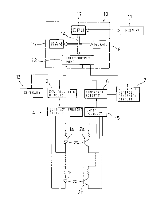
Fig. 1 is a schematic block diagram of a circuit for
controlling an optical film detecting means in a photograph-
ic printer machine showing one embodiment of the present
invention. An electronic control circuit 10 is connected to
a display 11 and a keyboard 12. The display 11 is provided
for displaying screen messages indicative of detected infor-
mation from a film detecting means. The keyboard 12 is
manually operable for modifying the detected information on
the display.
The electronic control circuit 10 has various functions
for actuating a film feeder, guides, a scanner, an exposure
illumination source, optical filters, and other devices
which all are not shown. The electronic control circuit 10
also contains a control program for the film detecting
means.
In common, the action and setting of the optical film
detecting means are controlled by a timer (not shown) which
has been preset for start or interval actions of the photo-
graphic printer machine using the electronic control circuit
10. It would be understood that the film detecting means
can also be controlled by manual entry of commands through
2142319
the keyboard 12.
There are provided an input/output port 13, a bus
circuit 14, a RAM (random access memory) 15, a ROM (read
only memory) 16, and a CPU (central processing unit) 17.
The optical film detecting means comprises multiple
pairs of light emitters la and light receivers lb: for
example, light emitting diodes and pin-PD photodiodes re-
spectively, which are mounted at appropriate locations in
the photographic printer machine. Each pair of the diodes
of the film detecting means are denoted by ln and 2n in
Fig. 1.
The light emitters la to ln are actuated by an analog
control signal which is converted by a D/A converter circuit
3 from a digital output of the electronic control circuit 10
and fed via a constant current circuit 4.
The light receivers 2a to 2n deliver their respective
detection signals to an input circuit 5 where they are
processed before further transmitted to the electronic
control circuit 10. The output of the inpu~ circuit 5 is
fed en route to a comparator circuit 6 where it is compared
in magnitude with a reference voltage supplied from a refer-
ence voltage generator circuit 7 to produce comparison
signals H and L (high and low) which are then transmitted to
the electronic control circuit 10. The reference voltage of
the reference voltage generator circuit 7 is produced in
response to a corresponding signal fro~ the electronic
control circuit 10.
2142~19
The method of film detection with the optical film
detecting means according to the present invention is imple-
mented by the foregoing control circuit.
In a manual mode, a flow chart shown in Fig 2 is com-
menced by key entry action with the keyboard 12. An auto-
matic mode action starts when a start-up inspection mode of
the photographic printer machine is selected and accessed.
The action of the flow chart starts with Step Sl where the
film detecting means is initiated so that each light path
between the light emitter 1 and the light receiver 2 is not
blocked. This initial action may be executed by an unshown
transfer mechanism. If a film is in its loaded position, it
may be moved back to clear the light path.
At Step S2, the electronic control circuit 10 sends a
command signal to the reference voltage generator circuit 7
for temporal increase of the reference voltage. The in-
crease may substantially be equal to, but not limited to, 20
% of the reference voltage. It is determined depending on
sensitivity characteristics of the film detecting means so
that the intensity of transmitted light is decreased to 50 %
to 60 ~ when blocked by a film. This may be common to other
embodiments employing 20 ~ or 80 %.
It is then examined at Step S3 whether or not the
output of the light receiver 2 is at high level. If not,
the intensity of illumination of the light emitter 1 is in
creased at Step S4 until the output of the light receiver 2
shifts from low to high. The high and low outputs or H and
2142~19
L signals are indicative of above and below a reference
voltage level (a datum setting value) respectively which are
provisionally determined for the light receiver 1 as shown
in Fig. 3(a). The H and L signals represent the absence and
presence of a film respectively. Accordingly, when the
reference voltage level has been increased at Step S2, it is
examined whether the output is higher or lower than an
increased reference voltage.
When the output of the light receiver 2 is high, an
input current to the light emitter 1 is reduced at Step S5
until the output of the light receiver 2 turns to low. Upon
the output of the light receiver 2 shifting to low, the
input current of the light emitter 1 drops to a level for
generating an intensity of illumination which corresponds to
the L signal (and is registered).
More specifically, the current driver of the light
emitter 1 is set with an increased level of the reference
voltage rather than an original level. The increase of
current for causing the output voltage of the light receiver
2 to turn to high is applied for eliminating the effect of
hysteresis property of the film detecting means and detect-
ing a point where the output voltage of the light receiver 2
is shifted from high to low on the decay slope.
The reference voltage at the light receiver 2 is then
returned to the original level at Step S7. This series of
actions give the following verification.
The loading of a film is detected by the film detecting
2142~19
means as the film is being placed between the light emitter
1 and the light receiver 2. According to the embodiment,
the intensity of illumination of the light emitter 1 when
blocked is decreased to at least 50 % to 60 % even if the
film carries a lower density.
It is now assumed that the output voltage of the light
receiver 2 in response to the illumination of the light
emitter 1 is set to correspond to the original reference
voltage level (a datum setting value) as in the prior art.
In general, the light emitter 1 will deteriorate with time
and produce a decreased intensity of illumination after a
long-run service of the film detecting means, e.g. one or
two years, while the light receiver 2 remains unchanged in
the reference voltage level.
If so, the illumination of the light emitter 1 has to
be increased by manual adjustment which is considered a
troublesome task. Also, such erratic adjustment as to set
the reference voltage to a lower level may result in fault
action of the photographic printer machine, i.e. a detection
signal indicative of the presence of a film is released.
For eliminating such a fault action, the present inven-
tion allows the light emitter 1 to illuminate so that the
light receiver 2 produces a voltage output which is greater
by a given increment margin than the reference voltage.
The increment margin is preferably 20 % of the original
reference voltage. If the increment margin is S0 % or
greater, the output of the light receiver 2 remains overlev-
2142319
eled. Accordingly, since the loss of transmitted lightacross the film is 50 % to 60 %, the film detecting means
may correctly generate a detection signal indicative of no
presence of the film.
If the margin of the reference voltage is as small as
less than 10 %, it may easily be affected or offset by the
deterioration with time. We have thus determined an eligi-
ble margin of 20 % through a succession of experiments.
In brief, the current input to the light emitter 1 is
increased, while no film is loaded between the light emitter
1 and the light receiver 2 of the film detecting means, from
a low level to a high level sufficient for having the volt-
age output of the light receiver 2 greater than the refer-
ence voltage. As the reference voltage is modified, a
difference between the presence and absence of the film is
maintained at optimum. Therefore, the detection of any film
can be executed at a higher accuracy in response to loading
and unloading of the film.
According to the method of the preser.t invention, even
if the reference voltage of the film detecting means is
biased due to physical deterioration with time, the film
detecting means performs the foregoing routine procedure
before starting its main detecting action. In case that the
reference voltage is biased to low, the current input to the
light emitter 1 is modified so that the voltage output of
the light receiver 2 is 20 % higher than the reference
voltage. As the result, the difference between the two
2142319
voltage output levels across the reference voltage remains
unchanged while the actual voltage output being changed,
ensuring the accuracy of the film detecting action.
Embodiment 2
Fig. 4 is a schematic overall block diagram of a con-
trol circuit according to a second embodiment of the present
invention. As shown, the comparator circuit 6 and the
reference voltage generator circuit 7 of the first embodi-
ment are eliminated. Components identical to those of the
first embodiment are denoted by like numerals and will be
explained in no more details.
In this embodiment, the above two components are sub-
stituted with a modification of the program in the electron-
ic control circuit 10.
As shown in Fig. 5, the output voltage of the light
receiver 2 is examined whether or not it is high at Step S12
similar to Step S3. As the reference voltage is not in-
volved, the output voltage is compared with reference values
prepared and stored in the electronic control circuit 10 for
judging the level.
The two steps S13 and S14 thus correspond to Steps S4
and S5 of Fig. 2. While Step S15 is equivalent to S6, the
routine of Fig. 5 is distinguished by only the fact that the
comparison is based on a prepared set of the reference
values in a memory.
The current input to the light emitter 1 is increased
at Step S16. More specifically, the increase of the current
214231g
-
input is calculated by a computer so that it results in a 20
% increase of the voltage output. This action is identical
to the initial current setting of the first embodiment on
the light emitter 1 relative to the reference voltage. Even
if the output voltage of the light receiver 2 is biased with
time, it will hardly be critical because the current input
to the light emitter 1 is modified to offset the bias.
Embodiment 3
Fig. 6 is a schematic overall block diagram of a con-
trol circuit showing a third embodiment of the present
invention, As shown, the D/A converter circuit 3, constant
current circuit 4, input circuit 5, comparator circuit 6,
and reference voltage generator circuit 7 are all eliminat-
- ed. They are substituted with an amplifier circuit 8 which
is coupled between the outputs of the light receivers 2 and
the electronic control circuit 10.
The electronic control circuit 10 of this embodiment is
substantially composed of a microcomputer operable with
digital signals. The light emitters 1 and the light receiv-
ers 2 are however driven by analog signals and thus, there
are provided a group of a D/A converter and a signal ampli-
fier in the light emitter side and an A/D converter in the
light receiver side. Those components are not directly
related to the performance of the film detecting method of
the present invention and appear not in the drawing. No
appearance of the components are throughout the drawings of
the embodiments.
2142~19
In the third embodiment, the film detecting method is
conducted by modifying the gain of the amplifier circuit 8
as illustrated in a flow chart of Fig. 7. Similar to the
second embodiment, it is examined at Step S22 whether or not
the output voltage of the light receiver 2 supplied through
the amplifier circuit 8 is at high level or greater than a
corresponding reference value stored in the electronic
control circuit 10. If not, the gain of the amplifier 8 is
increased until the output voltage becomes at the high level
(Step S23).
Upon the output voltage reaching the high level, the
gain is reduced. When the output voltage is at low level,
the gain of the amplifier circuit 8 is observed and regis-
tered to the electronic control circuit 10 which in turn
determines and records a corresponding reference value. An
initial value which is higher by an increment margin than
the reference value is then assigned to the gain of the
amplifier 8. The increment margin is preferably 20 % as
well as of the first embodiment.
As the gain of the amplifier circuit 8 is increased,
the output voltage of the light receiver 2 becomes relative-
ly high while the illumination of the light emitter 1 re-
mains unchanged. This is equivalent to increase of the
illumination of the light emitter 1. Accordingly, the
action of the film detecting means will be executed at a
higher accuracy as initially modified without the use of a
film, similar to the first or second embodiment where the
2142319
-
margin is given to the light emitters 1.
Embodiment 4
Fig. 8 is a schematic block diagram of an overall
control circuit showing a fourth embodiment of the present
invention. As shown, an A/D converter circuit 9 is coupled
to the electronic control circuit 10 which performs a film
detecting method of this embodiment.
At Step S31 of Fig. 9 similar to Step S1 of the first
embodiment, a film loaded across the film detecting means is
removed to allow transmission of light. The step S32 fol-
lows for reading an output of the A/D converter circuit 9 as
a reference level data. The read output is then reduced to
a given level and recorded into the RAM 15 at Step S33. The
reduced level is preferably 80 % of the original level which
is eligible as described in the previous embodiments.
According to the film detecting method, the presence or
absence of a film is determined as shown Fig. 3(b). When no
film is loaded, it is judged that the output of the A/D
converter 9 is greater than the reference level thus to be
at high level. If a film is loaded and attenuates the
transmission of light, the output is lower than the refer-
ence level to be at low level. In other words, the output
has a margin of 20 % as compared with the reference level.
14