Sélection de la langue

Search

Sommaire du brevet 2143105 

Énoncé de désistement de responsabilité concernant l'information provenant de tiers

Une partie des informations de ce site Web a été fournie par des sources externes. Le gouvernement du Canada n'assume aucune responsabilité concernant la précision, l'actualité ou la fiabilité des informations fournies par les sources externes. Les utilisateurs qui désirent employer cette information devraient consulter directement la source des informations. Le contenu fourni par les sources externes n'est pas assujetti aux exigences sur les langues officielles, la protection des renseignements personnels et l'accessibilité.

Disponibilité de l'Abrégé et des Revendications

L'apparition de différences dans le texte et l'image des Revendications et de l'Abrégé dépend du moment auquel le document est publié. Les textes des Revendications et de l'Abrégé sont affichés :

  • lorsque la demande peut être examinée par le public;
  • lorsque le brevet est émis (délivrance).
(12) Brevet: (11) CA 2143105
(54) Titre français: DISSIPATEUR DE CHALEUR POUR DISPOSITIFS A SEMICONDUCTEUR
(54) Titre anglais: HEAT SINK ASSEMBLY FOR SOLID STATE DEVICES
Statut: Durée expirée - au-delà du délai suivant l'octroi
Données bibliographiques
(51) Classification internationale des brevets (CIB):
  • H01L 23/40 (2006.01)
  • H01L 23/34 (2006.01)
  • H01L 23/36 (2006.01)
(72) Inventeurs :
  • TATA, PETER D. (Etats-Unis d'Amérique)
  • RIFE, WILLIAM B. (Etats-Unis d'Amérique)
(73) Titulaires :
  • TYCO ELECTRONICS LOGISTICS AG
(71) Demandeurs :
  • TYCO ELECTRONICS LOGISTICS AG (Suisse)
(74) Agent: SMART & BIGGAR LP
(74) Co-agent:
(45) Délivré: 1996-12-31
(86) Date de dépôt PCT: 1994-02-14
(87) Mise à la disponibilité du public: 1994-09-15
Requête d'examen: 1995-02-22
Licence disponible: S.O.
Cédé au domaine public: S.O.
(25) Langue des documents déposés: Anglais

Traité de coopération en matière de brevets (PCT): Oui
(86) Numéro de la demande PCT: PCT/US1994/001510
(87) Numéro de publication internationale PCT: US1994001510
(85) Entrée nationale: 1995-02-22

(30) Données de priorité de la demande:
Numéro de la demande Pays / territoire Date
08/026,515 (Etats-Unis d'Amérique) 1993-03-04
08/097,483 (Etats-Unis d'Amérique) 1993-07-26

Abrégés

Abrégé anglais


A heat sink assembly (10) adapted for use with an electronic device package
(24) such as a microprocessor having a grid array is shown having, in a first
embodiment a threaded base (34) of a finned heat sink (28) adapted to be received
in a threaded bore (26) of an adaptor (12) which mounts onto the electronic device
package (24). Desired thermal coupling is achieved by screwing down the heat sink
(28) in biasing engagement with the package (24). Alternate embodiments show theheat sink (28) which has a snap on flange (20, 22) to attach the heat sink (28) to the
adaptor (12) and the adaptor extending down to engage with the socket (60) in
which the electronic device package (24) is installed.

Revendications

Note : Les revendications sont présentées dans la langue officielle dans laquelle elles ont été soumises.


THE EMBODIMENTS OF THE INVENTION IN WHICH AN EXCLUSIVE
PROPERTY OR PRIVILEGE IS CLAIMED ARE DEFINED AS FOLLOWS:
1. A heat sink assembly for removing heat from an
electronic device package comprising
an adaptor having a top wall and having a pair of
opposed side walls depending downwardly therefrom, a groove
formed in each side wall extending generally parallel to the
top wall in alignment with and facing each other and being
capable of slidably receiving said electronic device package,
first and second planes lying respectively in the top and
bottom of the grooves defining a space therebetween, the
groove being adapted to clampingly receive opposite marginal
portions of an electronic device package when inserted
therein, a bore centrally located in the top wall and
extending therethrough,
a heat sink member having a cylindrical base member
having a longitudinal axis and with a flat bottom surface
adapted to be received through the bore in the top wall, the
base member formed with means to engage with the periphery of
the bore to secure and to attach the heat sink member to the
adaptor with the flat bottom surface disposed in the space
between the first and second planes whereby an electronic
device package slidably inserted in the grooves will cause the
top wall to bow through engagement with the flat bottom
surface of the base.
2. A heat sink assembly according to Claim 1 in which
the means to attach the heat sink member to the adaptor
- 6 -

comprises a circular flange extending radially outwardly from
the base member, the flange having a diameter slightly larger
than the bore in the top wall and having a tapered edge
portion to facilitate insertion of the base member through the
bore and to serve as a cam surface to force the base upwardly
and concomitantly the top wall to bow when an electronic
device package is inserted in the grooves; said base member
being in communication with the periphery of said bore to
secure said base member to the adaptor.
3. A heat sink assembly according to Claim 1 in which
the means to attach the heat sink member to the adaptor
comprises a male thread formed on the base member and a female
thread formed in the bore of the top wall to directly
threadably receive the base member.
4. A heat sink assembly according to Claim 1 including
a stop surface depending downwardly from the top wall to limit
the sliding travel in a direction perpendicular to the
longitudinal axis of said base member of an electronic device
package inserted in the grooves.
5. A heat sink assembly according to Claim 1 in which
the heat sink comprises a plurality of generally circular fin
members spaced along a generally cylindrical core and
extending radially therefrom.
6. A heat sink assembly according to Claim 3 in which
the bottoms of the grooves lie in a plane that is at a
- 7 -

selected distance from the upper surface of the top wall and
the thread formed on the cylindrical base member extends for a
distance along the longitudinal axis of the base member a
distance less than the selected distance to prevent excessive
forces from being exerted on the electronic device package.
7. A heat sink assembly according to Claim 3 in which
the top wall is formed with a boss portion having a greater
thickness than the remainder of the top wall, the threaded
bore extending through the boss portion to threadably receive
said base member to enable said base member to extend slightly
below said top wall to provide frictional communication with
said electronic device package.
8. A heat sink assembly for removing heat from an
electronic device package having an outer peripheral edge and
an array of pins comprising
an adaptor having a top wall and having a pair of
opposed side walls depending therefrom, each side wall having
a distal end portion and having an inwardly laterally
extending lip, forming a groove adapted to receive between
each lip and the top wall a marginal portion of an electronic
device package inserted therein, a threaded bore formed
through the top wall, each of said lips extend inward a
distance less than the distance from the outer edge of said
electronic device package to said pins; and
a heat sink member having a threaded base portion
with a substantially flat bottom surface adapted to be
threadably received in the threaded bore in the top wall
- 7a -

whereby the base of the heat sink can be screwed down through
the bore in the top wall with a flat bottom surface in
engagement with a top surface of the electronic device package
received in the adaptor.
9. A heat sink assembly according to Claim 8 in which
the top wall of the adaptor has a selected thickness and the
threaded base portion has a longitudinal axis, the threaded
base portion of the heat sink having a length taken along the
longitudinal axis greater than the selected thickness to
enable it, upon being screwed down, to exert sufficient
pressure on the top surface of the electronic device to secure
the assembly on the electronic device package.
10. A heat sink assembly according to Claim 8 in which
the heat sink comprises a plurality of generally circular fin
members spaced along a generally cylindrical core and
extending radially therefrom.
11. A heat sink assembly according to Claim 8 in which
the adaptor has a stop surface to limit sliding motion in a
direction perpendicular to the longitudinal axis of said base
portion of an electronic device package inserted into the
adaptor.
12. A heat sink assembly according to Claim 1 in which
the heat sink comprises a continuous helically shaped fin
member extending radially outwardly from a core.
- 7b -

13. A heat sink assembly according to Claim 8 in which
the heat sink comprises a continuous helically shaped fin
member extending radially outwardly from a core.
- 7c -

14. A heat sink assembly according to Claim 1 in which the side walls have a lower distal
end portion formed with a tapered surface so that the adaptor can be pushed downwardly onto an
electronic device package with the tapered surfaces camming the side walls apart to allow the
electronic device package to pass by the tapered surface; said adaptor being capable of being pushed
downwardly onto an electronic device package when the heat sink member is not threaded into the
bore in the top wall and when said heat sink member is partially threaded into said bore to provide
pressure onto the top surface of the electronic device package to secure the assembly to the
electronic device package.
15. A heat sink assembly according to Claim 8 in which a tapered surface is formed on the
distal end portions of the side walls so that the adaptor can be pushed downwardly onto an
electronic device package with the tapered surfaces camming the side walls apart to allow the
electronic device package to pass by the tapered surface; said adaptor being capable of being pushed
downwardly onto an electronic device package when the heat sink member is not threaded into the
bore in the top wall and when said heat sink member is partially threaded into said bore to provide
pressure onto the top surface of the electronic device package to secure the assembly to the
electronic device package.
16. A heat sink assembly for removing heat from an electronic device package comprising
an adaptor having a top wall and having a pair of opposed side walls depending downwardly
therefrom to a lower distal end portion a lip extending laterally inwardly from each lower distal
end portion aligned with and facing each other, an aperture formed in the top wall extending
therethrough, said adaptor being capable of slidably receiving the electronic device package;
a heat sink member having a base member with a flat bottom surface adapted to be received
through the aperture in the top wall, the base member formed with means to directly engage the
periphery of the aperture to secure and to attach the heat sink member to the adaptor with the flat
bottom surface disposed below the top wall whereby an electronic device package held between the
side walls above the lips will be disposed in heat transfer relation with the heat sink member.
17. A heat sink assembly according to Claim 16 in which the base member and the aperture
are generally cylindrical and the means to attach the heat sink member to the adaptor comprises a
male thread formed on the base member and a female thread formed in the aperture in the top wall
to threadably receive the base member.
18. A heat sink assembly according to Claim 16 in which the means to attach the heat sink
member to the adaptor comprises a flange extending outwardly from the base member, the flange
having an outer configuration shaped to correspond to that of the aperture but being slightly larger
than the aperture and having a tapered edge portion to facilitate insertion of the base member
through the aperture: whereby the base member is attached to the periphery of said aperture to
secure the base member to the adaptor.

19. A heat sink assembly according to claim 16 in which
the lips on the lower distal end portions of the side walls
are formed with a tapered surface so that the adaptor can be
pushed downwardly onto an electronic device package with the
tapered surfaces camming the side walls apart to allow the
electronic device package to pass by the lips said adaptor
being capable of being pushed downwardly onto an electronic
device package when the heat sink member is not threaded into
the bore in the top wall and when said heat sink member is
partially threaded into said bore to provide pressure onto the
top surface of the electronic device package to secure the
assembly to the electronic device package.
20. A heat sink assembly for removing heat from an
electronic device package comprising
an adaptor having a top wall and having a pair of spaced
side walls depending downwardly therefrom to a lower distal
end protion, a lip extending laterally inwardly from each
lower distal end portion, an aperture formed in the top wall
extending therethrough,
a heat sink member having a base member with a flat
bottom surface adapted to be received through the aperture in
the top wall, the base member formed with means to directly
engage with the periphery of the aperture to secure and to
attach the heat sink member to the adaptor with the flat
bottom surface disposed below the top wall whereby an
electronic device package held between the side walls above
the lips will be disposed in heat transfer relation with the
heat sink member.
-9-

21. A heat sink assembly according to claim 20 in which
the base member and the aperture are generally cylindrical and
the means to attach the heat sink member to the adaptor
comprises a male thread formed on the base member and a female
thread formed in the aperture.
22. A heat sink assembly for removing heat from an
electronic device package installed in a socket on a circuit
board comprising
an adaptor having a top wall and having a pair of
opposed side walls depending downwardly therefrom, a groove
having a top and a bottom formed in each side wall extending
generally parallel to the top wall in alignment with and
facing each other and being capable of slidably receiving said
electronic device package and said socket simultaneously, said
groove formed in each side wall having a width slightly
greater than the combined thickness of said electronic device
package and said socket, first and second planes lying
respectively in the top and bottom of the grooves defining a
space therebetween, the groove being adapted to clampingly
receive opposite marginal portions of both a socket and
electronic device package inserted in said socket, a bore
centrally located in the top wall and extending therethrough,
a heat sink member having a cylindrical base member
with a flat bottom surface adapted to be received through the
bore in the top wall, the base member formed with means to
engage with the periphery of the bore to secure and to attach
the heat sink member to the adaptor with the flat bottom
surface disposed in
- 10 -

11
the space between the first and second planes whereby an
electronic device package installed in a socket slidably
inserted in the grooves will cause the top wall to bow through
engagement with the flat bottom surface of the base.
23. A heat sink assembly according to claim 22 in which
the means to attach the heat sink member to the adaptor
comprises a circular flange extending radially outwardly from
the base member, the flange having a diameter slightly larger
than the bore in the top wall and having a tapered edge portion
to facilitate insertion of the base member through the bore and
to serve as a cam surface to force the base upwardly and
concomitantly the top wall to bow when a socket and electronic
device package installed therein are inserted in the grooves;
said base member being in communication with the periphery of
said bore to secure said base member to the adaptor.
24. A heat sink assembly according to claim 22 in which
the means to attach the heat sink member to the adaptor
comprises a male thread formed on the base member and a female
thread formed in the bore of the top wall to directly threadably
receive the base member.
25. A heat sink assembly according to claim 22 including a
stop surface depending downwardly from the top wall to limit the
sliding travel in a direction perpendicular to the longitudinal
axis of said base member of a socket and electronic device
package inserted in the grooves.

12
26. A heat sink assembly according to claim 22 in which
the heat sink comprises a plurality of generally circular fin
members spaced along a generally cylindrical core and extending
radially therefrom.
27. A heat sink assembly according to claim 24 in which
the plane extending through the bottom of the grooves is a
selected distance from the upper surface of the top wall and the
thread formed on the cylindrical base member extends for a
distance along the longitudinal axls of the base member a
distance less than the selected distance to prevent excessive
forces from being exerted on the electronic device package.
28. A heat sink assembly according to claim 24 in which
the top wall is formed with a base portion having a greater
thickness than the remainder of the top wall, the threaded bore
extending through the base portion to threadably receive said
base member to enable said base member to extend slightly below
said top wall to provide frictional communication with said
electronic device package.
29. A heat sink assembly for removing heat from an
electronic device package having an outer peripheral edge and an
array of pins installed in a socket capable of receiving said
pins on a circuit board comprising
an adaptor having a top wall and having a pair of opposed
side walls depending therefrom, each side wall having a distal
end portion and having an inwardly laterally extending lip,

13
forming a groove adapted to receive between each lip and the top
wall the marginal portions of a socket and electronic device
package arrangement inserted therein, said groove formed in each
side wall having a width slightly greater than the combined
thickness of said electronic device package and said socket, a
threaded bore formed through the top wall, said socket and
electronic device package arrangement including an electronic
device package installed into said socket; each of said lips
extending inward a distance less than the distance from the
outer edge of said electronic device package to said pins; and
a heat sink member having a threaded base portion with a
substantially flat bottom surface adapted to be threadably
received in the threaded bore in the top wall whereby the base
of the heat sink can be screwed down through the bore in the top
wall with a flat bottom surface in engagement with a top surface
of the electronic device package installed in the socket and
received in the adaptor.
30. A heat sink assembly according to claim 29 in which
the top wall of the adaptor has a selected thickness and the
threaded base portion has a longitudinal axis, the threaded base
portion of the heat sink having a length taken along the
longitudinal axis greater than the selected thickness to enable
it, upon being screwed down, to exert sufficient pressure on the
top surface of the electronic device to secure the assembly on
the electronic device package.
31. A heat sink assembly according to claim 29 in which

14
the heat sink comprises a plurality of generally circular fin
members spaced along a generally cylindrical core and extending
radially therefrom.
32. A heat sink assembly according to claim 29 in which
the adaptor has a stop surface to limit sliding motion in a
direction perpendicular to the longitudinal axis of said base
portion of the socket and electronic device package arrangement
inserted into the adaptor.
33. A heat sink assembly according to claim 22 in which
the heat sink comprises a continuous helically shaped fin member
extending radially outwardly from a core.
34. A heat sink assembly according to claim 29 in which
the heat sink comprises a continuous helically shaped fin member
extending radially outwardly from a core.
35. A heat sink assembly according to claim 22 in which
the side walls have a lower distal end portion formed with a
tapered surface so that the adaptor can be pushed downwardly
onto an electronic device package installed in a socket with the
tapered surfaces camming the side walls apart to allow the
electronic device package and said socket to pass by the tapered
surface; said adaptor being capable of being pushed downwardly
onto an electronic device package installed in a socket when the
heat sink member is not threaded into the bore in the top wall
and when said heat sink member is partially threaded into said

bore to provide pressure onto the top surface of the electronic
device package to secure the assembly to the electronic device
package.
36. A heat sink assembly according to claim 29 in which a
tapered surface is formed on the distal end portions of the side
walls so that the adaptor can be pushed downwardly onto an
electronic device package installed in a socket with the tapered
surfaces camming the side walls apart to allow the electronic
device package and socket to pass by the tapered surface; said
adaptor being capable of being pushed downwardly onto an
electronic device package installed in a socket when the heat
sink member is not threaded into the bore in the top wall and
when said heat sink member is partially threaded into said bore
to provide pressure onto the top surface of the electronic
device package to secure the assembly to the electronic device
package.
37. A heat sink assembly for removing heat from an
electronic device package installed in a socket on a circuit
board comprising
an adaptor having a top wall and having a pair of opposed
side walls depending downwardly therefrom to a lower distal end
portion, a lip extending laterally inwardly from each lower
distal end portion aligned with and facing each other, an
aperture formed in the top wall extending therethrough, said
adaptor having a receiving aperture with a width slightly
greater than the combined thickness of said electronic device

package and said socket, said adaptor being capable of
slidably receiving the electronic device package and said
socket simultaneously in said receiving aperture,
a heat sink member having a base member with a flat
bottom surface adapted to be received through the aperture in
the top wall, the base member formed with means to directly
engage the periphery of the aperture to secure and to attach
the heat sink member to the adaptor with the flat bottom
surface disposed below the top wall whereby an electronic
device package and socket held between the side walls above
the lips will be disposed in heat transfer relation with the
heat sink member.
38. A heat sink assembly according to claim 37 in which
the base member and the aperture are generally cylindrical and
the means to attach the heat sink member to the adaptor
comprises a male thread formed on the base member and a female
thread formed in the aperture in the top wall to threadably
receive the base member.
39. A heat sink assembly according to claim 37 in which
the means to attach the heat sink member to the adaptor
comprises a flange extending outwardly from the base member,
the flange having an outer configuration shaped to correspond
to that of the aperture but being slightly larger than the
aperture and having a tapered edge portion to facilitate
insertion of the base member through the aperture; whereby the
base member is attached to the periphery of said aperture to
secure the base member to the adaptor.
- 16 -

17
40. A heat sink assembly according to claim 37 in which
the lips on the lower distal end portions of the side walls are
formed with a tapered surface so that the adaptor can be pushed
downwardly onto an electronic device package installed in a
socket with the tapered surfaces camming the side walls apart to
allow the electronic device package and socket to pass by the
lips; said adaptor being capable of being pushed downwardly onto
an electronic device package installed in a socket when the heat
sink member is not threaded into the bore in the top wall and
when said heat sink member is partially threaded into said bore
to provide pressure onto the top surface of the electronic
device package to secure the assembly to the electronic device
package.
41. A heat sink assembly for removing heat from an
electronic device package installed in a socket on a circuit
board comprising
an adaptor having a top wall and having a pair of spaced
side walls depending downwardly therefrom to a lower distal end
portion, a lip extending laterally inwardly from eacn lower
distal end portion, an aperture formed in the top wall extending
therethrough,
a heat sink member having a base member with a flat bottom
surface adapted to be received through the aperture in the top
wall, the base member formed with means to attach the heat sink
member to the adaptor with the flat bottom surface disposed
below the top wall whereby an electronic device package and
socket held between the side walls above the lips will be

disposed in heat transfer relation with the heat sink member.
42. A heat sink assembly according to claim 41 in which
the base member and the aperture are generally cylindrical and
the means to attach the heat sink member to the adaptor
comprises a male thread formed on the base member and a female
thread formed in the aperture.
43. A heat sink assembly for removing heat from an
electronic device package installed in a socket on a circuit
board comprising
an adaptor having a top wall and having a pair of
opposed side walls depending downwardly therefrom, a groove
having a top and a bottom formed in each side wall extending
generally parallel to the top wall in alignment with and
facing each other, said groove formed in each side wall having
a width slightly greater than the combined thickness of said
electronic device package and said socket, and being capable
of slidably receiving said electronic device package and said
socket simultaneously, first and second planes lying
respectively in the top and bottom of the grooves defining a
space therebetween,
means for securing said adaptor on the electronic
package,
a bore centrally located in the top wall and
extending therethrough,
a heat sink member having a cylindrical base member
with a flat bottom surface adapted to be received through the
bore in the top wall, the base member formed with means to
- 18 -

engage with the periphery of the bore to secure and to attach
the heat sink member to the adaptor with the flat bottom
surface disposed in the space between the first and second
planes whereby an electronic device package installed in a
socket slidably inserted in the grooves will cause the top
wall to bow through engagement t with the flat bottom surface of
the base.
44. A heat sink assembly according to claim 43 in which
the means to attach the heat sink member to the adaptor
comprises a male thread formed on the base member and a female
thread formed in the bore of the top wall to directly
threadably receive the base member.
45. A heat sink assembly according to claim 43 including
a top surface depending downwardly from the top wall to limit
the sliding travel in a direction perpendicular to the
longitudinal axis of said base member of a socket and
electronic device package inserted in the grooves.
- 19 -

Description

Note : Les descriptions sont présentées dans la langue officielle dans laquelle elles ont été soumises.


WO 94120987 21431~ 5 PCTIUS94101510
llEAT SINK ASSEMBLY FOR SOLi~ STATE DEVICES
TECHi~iC~I FIFI.T) ~,
This invention reiates generail~ to electronic solid state devices and more partieularly. to
apparatus for dissipating heat generated by such devices.
As advances are made in the electronics industr~ with more funchons provided in smaller
arehiteeture, the effieient removai of heat beeomes inereasingly important. Solid state devices. sueh
as . and the liice, generate a great deal of heat during operahon which must be
removed to prevent adverse effeets on operation of the system in whieh the solid state deviee is used
amd e~en self-destruebon of the deviee or destruction of near-by components.
BACKGROUi~D ART
It is icnown to thermally couple heat sini~s wi~h such de~ices in order to dissipate heat
generated by the devices and, consequently, lo~er the lemperature of the devices to safe limits. One
example of such a heat sink is shown and described in U.S. Patent No. 4,745,456. In tilat patent, a
fimned heat sinic comprising a central post having a plurality of spaced fins extending radially from
the post is seeured to an eleetronic device package by means of a ciip which attaches to a latch
mechanism on a frame in which the device paci~age is held and which releasably grips the heat sini~
and urges it into engagement with the device paci~age. This structure, while effeeti~e v~hen the
clamping foree biases the heat sink into firm engagemeM with the eleetronic deviee paei~age, tends
to be ineonsistent as the semi-eonduetor heats up and, at elevated ' . , the foree biasing
the heat sini~ against the de~ice paci~age ean decrease maicing the thermal path less efficient. In
fact, apparently due to differences in the thermal expansion of the severai parts~ the thermal
eoupling betv~een the heat sink amd the device paci~age ean be significamtiy diminished eaused by a
siight tilting of the heat sink sarface to break the plane to plane contaet of the heat sinic core v~lth
the top surface of the eleetronic device paei~age. Even ~vhen thermal grease is placed between the
2s heat sink and the device paci~age, it is foand that thermal coupling can be significantly reduced
uith the resalt that the de lce package o ~erheats and causes deietenous operational effects.
Heat sinks have also been permanentlv bonded to the electronic device pacicage to provide an
efficient thermal coupling bet~veen the tv.o components: ho~vever, over time the bond tends to break
thereby adversely affecting the thermal path between the heat sini~ and the de~ice paci~age.
Another approach to preventing overheahng has been to moant a smail fan on the heat sini~
to increase thermal dissipation of the heat sink. While this ean be very effective in maintaining the
tempeMture of the device paekage to acceptable levels, it is not only costly if opeMtion of the fan is
interrupted due to some maifunction, but the device ~vill be ineffective to pre~ent un~vanted
tempeMture rise.
3s It is an object of the present invention to pro-~ide a heat sink assembl~ for removing heat
from an electronic device which is reliable ~et ine.cpensive. one which ob iates the limitations of
the prior art mentioned abo ~e.
.

6UMMARY OF THE INVENTION 2 1 4 3 1 0 5
The lnventlon provldes a heat slnk assembly for
remov~ng heat from an electronlc devlce package lnstalled ln a
socket on a clrcult board comprlslng an adaptor havlng a top
wall and havlng a palr of spaced glde wallg ~lorc-nrlln~
downwardly therefrom to a lower distal end portlon, a lip
extendlng laterally lnwardly from each lower dlstal end
portlon, an aperture formed ln the top wall extendlng
therethrough, a heat slnk member havlng a base member wlth a
f lat bottom surface adapted to be recelved through the
aperture ln the top wall, the base member formed wlth means to
attach the heat slnk member to the adaptor wlth the flat
bottom surface dlsposed below the top wall whereby an
electronlc devlce package and socket held between the slde
walls above the llps wlll be disposed ln heat transfer
relatlon wlth the heat slnk member.
Brle~ly, in accordance with a f lrst ~ r - t of
the lnventlon, the heat slnk member 18 formed with a threaded
base wh~ ch 18 adapted to be recelved ln a threaded bore ~ormed
in the top wall of the adaptor which is adapted to clamp
spaced marglnal edges of an elect ronlc devlce package . The
package 18 lnserted into opposed grooves of the adaptor and
then the heat slnk, whlch may be of varlous conflguratlons
including the type having a plurality of generally clrcular
fins spaced along a generally cyllndrlcal core or a hellcal
fln e~tendlng from the core, 18 screwed down toward the
package untll the flat bottom surface of the heat slnk base 18
flrmly blased agalnst the top of the electronlc devlce package
and thermally coupled thereto. The adaptor, lf deslred, may
-- 2 --
C~ 21519-648(8)
. , .. . , . . , ... :, . . , . .. _ . _ . . . , _ _,, _, . ... . . ...... . ... .......

~ 2t ~31 o5
be provlded wlth a downwardly extendlng stop surface to llmlt
travel of an electronlc devlce package lnserted lnto the
grooves and locate the threaded bore at a central locatlon of
the package . In a modlf led embodlment, the top wall of the
adaptor 18 formed wlth a thlcker hub portlon through whlch the
bore extends ln order to provlde a longer threaded bore for
the threaded base. In an alternat~ve ~ ', the base 18
provlded wlth an outwardly extendlng f lange at lts lower
dlstal end and 18 provlded wlth a tapered surface port lon .
The flange 18 adapted to snap through the bore ln the top wall
to lock the heat slnk to the adaptor. The tapered surface
portlon also serves as a cam surface when an electron~c devlce
package 18 lnserted ln the grooves blaslng the base upwardly
80 that there 18 a good thermal coupllng therebetween. In yet
another embodlment, the lower port lon of the grooves are
formed wlth llps havlng a tapered or cam curve surface 80 that
the adaptor can be pushed onto an electronlc devlce package
wlth the llps snapplng over the opposlte marglnal edges of the
package .
Varlous ob~ects and advantages of the present
lnventlon wlll become apparent from the followlng detalled
descrlpt lon and accompanylng drawlngs .
~RIEF DESCRIPTION OF THE DRAWINGS
In the accompanylng drawlngs ln whlch several of the
pre~erred embodlments of the lnventlon are lllustrated
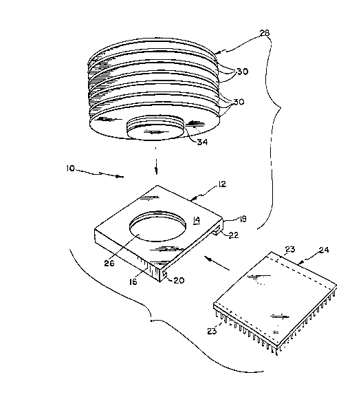
Flg . 1 18 a broken apart perspect lve vlew of a heat
slnk assembly made ln accordance wlth a f lrst : ~ -11 r-~lt of
the lnventlon comprlslng a heat slnk member and an adaptor
shown along wlth an electronlc devlce package ln the form of a
- 2a -
r~ 21519-648(S)
_ . .. .. . .. . . . . .. _ .. _ . _ . . . ... . _ . . _ . , _ = . _ . . _ . . . .. .. _

~ ~ 2143105
mlcroprocessor having a grld array;
Flg. 2 18 a slde elevatlon of the Flg. 1 apparatus
wlth the adaptor shown ln cross sectlon;
Flg. 3 18 a top plan vlew of the Flgs. 1, 2 adaptor.
Flg. 4 18 a slde elevatlon of a modlfled adaptor~
Flgs . 5 and 6 are side elevat lonal vlews, the
adaptor shown ln cross sectlon of an alternatlve: -~lr ' of
the lnventlon before and after connectlng the heat slnk to the
adapt o r .
Fls~s. 7 and 8 are top plan and cross sectlonal vlews
of an adaptor of yet another ~ ` ~rllr- ' of the lnvention7
Flg. 9 18 a perspectlve vlew, partly ln cross
section, of a heat slnk havlng a contlnuous
- 2b -
~; 21519-648(S)

~ WO 94no987 ~ 31~ 5 PCTNS94/01510
helical fin useful with the adaptor of the invention;
hg. 10 is a top plan view of a modified hea~ sinic adaptor; and
Fig. Il isacrosssectionalvieu~takenonline 11-11 of Fig. 10.
Fig. 12 is a cross sectionai view of an alternative embodiment of the present in~ ention taken
5 aiong a line through the heat sink core and ~ h,~ . to the path of insertion.
MODES FOR CARRYlNG OuT THE INVENTION
According to a first embodiment of the invenbon, as shown in Figs. 1-3, a heat sink
assembl~ 10 for an electronic device package containing a solid state de ice such as a
, or the like, comprising an adaptor 12 formed of an electricaily insuiauve matenal,
such as an Ai3S piastic. ha~ing a top wall 14 and opposed side wall 16, 18 depending therefrom.
Side walls 16, 18 are formed with lateraily inwardly extending lips 20, 22 at their respective distal
end portions forming a groove with top wall 14 adapted to capture the outer extremities or marginal
portions of a solid state de~ice 24. Top wall 14 is formed with a centrally disposed threaded bore
26. If desired a stop wall 19 can be provided depending downwardly from the back side of the
adaptor to conveniently center the solid state device relative to bore 26. Stop wall 19 is shown with
an optional in~vardiy extending lip 21.
Heat sink 28, formed of good thermally conductive matenal such as aluminum. compnses a
pluraliy of thin members 30 extending integrally from a core 32 having a threaded base 3~ adapted
to be threadingly received in a threaded bore 26.
Soiid state device 24, such as a , having a gate array, is inserted into adaptor12 with the outer marginal portions of the housing of de~ice 24. shown in Fig. I b~ dash lines 23,
received between lips 20, 22 and top wall 14 and the stop wall 19 limiting the in~vard mohon of
device 24 so that threaded bore 26 is aligned with the central portion of device 24. Heat sink 28 is
tben screwed into threaded bore 26 until it bonoms out against the solid state device 24 in inbmate
thermal coupling therewith. The flat bonom surface of base 34 is adapted to be placed on the space
formed by planes Iying respecdvely in the top and bottom of the surfaces forming the grooves to
ensnre a good thermal coupling with a solid state device received tilereitt. Threaded bore 34 of the
heat sinic e.ctends l v' " "~ a distance preferably slightly longer than the distance bet- een top
wall 14 and the top surface of a device 24 placed within the adaptor so that the heat sink can be
screwed in until top wall bo~s slightl- biasing the heat sink against solid state de~ice 12. If
desired, the longitudinal length of the thread on the heat sink base can be selected to extend a
certain length to limit downward travel of the heat sink in order to prevent excessi~e forces from
being placed on the electronic device package. Generally, it is desirable to place sonle thermall~
conductive grease, such as a silicon based grease or a flexible heat conductive tape~ bel~ een base 34
3 5 and solid state de~ice 24 to further enhance heat flow.
Due to the stress placed on the adaptor bv scre~ing the heat sink against the solid state
de~ice, the Fig. I structure ~ ill maintain a bias of the heat sink against the solid state device. and

WO 94/20987 PCT/US94/01510 J
21~310~
thus an efficient heat path, even when the solid state device heats up.
Although an electrically insulative matenal is convenient to use since shoning of the pins of
the solid state device member is obviated, metal can also be used to form adaptor 12 with lips 20,
21 and 22 coating with a layer of suitable electrically insulative matenal,
s In a modification of the Figs. 1-3 embodiment shown in Fig. 4, a boss 40 can be formed on
the top wall of adaptor 12' to form a longer axial length of threaded bore 26' to facilitate the
attachment between the adaptor and the heat sink.
Another embodiment, shown in Fig. 5, provides a snap coupling of heat sink 28' to adaptor
12". Base 34' has a tapered flange 42 adapted to be forced through bore 26' until the radially
extending lip 44 snaps beyond recessed surface 46. In order to optimize thermal coupling between
hQt sink 28' and solid state devioe 24, the vendcal heighl of tapered flange 42, shown as "a'' in hg.
5, may be selected to be slightly more than the distance between recess snrface 46 and the lower
surface 48 of top wall 14". This will cause the lower surface 50 of heat sink 28' to be disposed in
the space where the housing of solid state device 24 would occupy when insened in the adaptor so
tbat the tapered surface of flange 42 will cam wall 14 to bow it upwardly as solid state device 24 is
pushed into the adaptor thereby insuring an efficient thermal coupling even with changes in
temperature. Althongh heat sink 28' is shown formed with a cylindrical base it will be appreciated
that it is within the purview of the invention to provide other ~,, , if desired such as
oblong or rectangular with a ~ . '' ,, configured flange and apenure in the top wall.
Figs. 7 and 8 show another embodiment of the invention in which adaptor 12"' is provided
with lips 20', 22' which have tapered surfaces 20.1, 22.1 respectively so that the adaptor can be
placed on top of a solid state device 24 and pushed down onto it with surfaces 20.1 and 22.1 acting
as cam surfaces forcing side walls 16', 18' to spread apart with the side walls 16', 18' returning to
their normal vertical onentaùon when lips 20', 22' pass beyond the lower edge of solid state device
2s 24 to securely grasp device 24. When a heat sink, such as heat sink 28" shown in Fig. 9 is screwed
into bore 26 and into engagement with a solid state device 24 held in adapter 12"', the grasping
force will be increased as top wall 14"' starts to bow upwardly. As seen in Fig. 7, stop wall 14"' is
provided with cut out portions 14.1 to enhance de~elopment of spring like I - t ;~ ` to the
wall.
Heat sink 28'' of Fig. 9 is similar to heat sink 28 and 28' shown in the previous figures but
instead of having a plurality of separate fin members 30, has a single helical fin 30' integrall
forrned with core 32.
Figs. 10 and 11 show a modifled heat sink in which spaced apart grooves are formed on two
contiguous sides of the adaptor by lips 22.2 and 21.2 which are adapted to be received under spaced
3s marginal portions of device package 24 to firml~ grasp the package when a heat sink is inserted in
bore 26 and screwed down into engagement with the package.

21431~
~ WO 94120987 PCTIUS94/01~10
s
Turning now to Fig. 12, an aiternative embodiment of the present invention is shown. ~ieat
sink 2~ with fins 30 is engaged witb adaptor 12 which has extended legs 68. Soiid state device 24
is instailed in socket 60 via pins 62. Socket 60 is in turn connected, in permanent fashion, to
circnit board 66 via soldered pins 64. In this embodiment, legs 68 are extended so that lips 20 and
22 may engage with the bottom surface of socket 60. The embodiment of Fig. 12 is panicularl)
useful for successfully dissipating heat in vertically mounted solid state devices 24. When a heat
sink 2X or other heat dissipating member is affixed to tbe surface of a solid state device which is
verticaily mounted, the waght of the heat sini~ gradually pulls the solid state device 24 out of its
socket 60. This results in poor connection of the solid state device and bending of pins 62. As
shown in hg. 12, legs 68 grip onto socket 60 via lips 20 and 22 to place the weight on soldered
socket 60 wilich provides a better mount for the heat sink assembly in a vertically mounted solid
state device.
Aithough the invention has been descnbed with respect to specific preferred
thereof, variations and r '' will become apparent to those skilled in the art. It is therefore
the intention that the appended ciaims be interpreted as broadly as possible in view of the prior art
to include all such vanations and "~ '

Dessin représentatif
Une figure unique qui représente un dessin illustrant l'invention.
États administratifs

2024-08-01 : Dans le cadre de la transition vers les Brevets de nouvelle génération (BNG), la base de données sur les brevets canadiens (BDBC) contient désormais un Historique d'événement plus détaillé, qui reproduit le Journal des événements de notre nouvelle solution interne.

Veuillez noter que les événements débutant par « Inactive : » se réfèrent à des événements qui ne sont plus utilisés dans notre nouvelle solution interne.

Pour une meilleure compréhension de l'état de la demande ou brevet qui figure sur cette page, la rubrique Mise en garde , et les descriptions de Brevet , Historique d'événement , Taxes périodiques et Historique des paiements devraient être consultées.

Historique d'événement

Description Date
Inactive : Périmé (brevet - nouvelle loi) 2014-02-14
Inactive : Grandeur de l'entité changée 2004-01-09
Lettre envoyée 2001-06-21
Accordé par délivrance 1996-12-31
Exigences pour une requête d'examen - jugée conforme 1995-02-22
Toutes les exigences pour l'examen - jugée conforme 1995-02-22
Demande publiée (accessible au public) 1994-09-15

Historique d'abandonnement

Il n'y a pas d'historique d'abandonnement

Historique des taxes

Type de taxes Anniversaire Échéance Date payée
TM (brevet, 4e anniv.) - petite 1998-02-16 1997-11-20
TM (brevet, 5e anniv.) - petite 1999-02-15 1998-11-13
TM (brevet, 6e anniv.) - petite 2000-02-14 2000-01-06
TM (brevet, 7e anniv.) - petite 2001-02-14 2000-11-09
Enregistrement d'un document 2001-05-30
Annulation de la péremption réputée 2003-02-14 2002-01-07
TM (brevet, 8e anniv.) - petite 2002-02-14 2002-01-07
Annulation de la péremption réputée 2003-02-14 2003-01-06
TM (brevet, 9e anniv.) - petite 2003-02-14 2003-01-06
TM (brevet, 10e anniv.) - générale 2004-02-16 2003-12-16
TM (brevet, 11e anniv.) - générale 2005-02-14 2005-01-20
TM (brevet, 12e anniv.) - générale 2006-02-14 2006-01-19
TM (brevet, 13e anniv.) - générale 2007-02-14 2007-01-17
TM (brevet, 14e anniv.) - générale 2008-02-14 2008-01-18
TM (brevet, 15e anniv.) - générale 2009-02-16 2009-01-19
TM (brevet, 16e anniv.) - générale 2010-02-15 2010-01-18
TM (brevet, 17e anniv.) - générale 2011-02-14 2011-01-17
TM (brevet, 18e anniv.) - générale 2012-02-14 2012-01-17
TM (brevet, 19e anniv.) - générale 2013-02-14 2013-01-17
Titulaires au dossier

Les titulaires actuels et antérieures au dossier sont affichés en ordre alphabétique.

Titulaires actuels au dossier
TYCO ELECTRONICS LOGISTICS AG
Titulaires antérieures au dossier
PETER D. TATA
WILLIAM B. RIFE
Les propriétaires antérieurs qui ne figurent pas dans la liste des « Propriétaires au dossier » apparaîtront dans d'autres documents au dossier.
Documents

Pour visionner les fichiers sélectionnés, entrer le code reCAPTCHA :


Pour visualiser une image, cliquer sur un lien dans la colonne description du document. Pour télécharger l'image (les images), cliquer l'une ou plusieurs cases à cocher dans la première colonne et ensuite cliquer sur le bouton "Télécharger sélection en format PDF (archive Zip)" ou le bouton "Télécharger sélection (en un fichier PDF fusionné)".

Liste des documents de brevet publiés et non publiés sur la BDBC .

Si vous avez des difficultés à accéder au contenu, veuillez communiquer avec le Centre de services à la clientèle au 1-866-997-1936, ou envoyer un courriel au Centre de service à la clientèle de l'OPIC.


Description du
Document 
Date
(aaaa-mm-jj) 
Nombre de pages   Taille de l'image (Ko) 
Abrégé 1994-09-14 1 52
Description 1994-09-14 5 283
Revendications 1994-09-14 9 483
Dessins 1994-09-14 4 73
Revendications 1995-06-21 9 483
Abrégé 1995-06-21 1 52
Dessins 1995-06-21 4 73
Description 1995-06-21 5 283
Description 1996-12-30 7 314
Abrégé 1996-12-30 1 19
Revendications 1996-12-30 17 635
Dessins 1996-12-30 4 64
Dessin représentatif 1999-05-20 1 16
Courtoisie - Certificat d'enregistrement (document(s) connexe(s)) 2001-06-20 1 112
Correspondance 2000-11-08 1 23
Taxes 2000-11-08 1 24
Taxes 1996-11-13 1 39
Taxes 1996-01-15 2 73
Demande d'entrée en phase nationale 2001-05-29 8 317
Demande d'entrée en phase nationale 1995-06-06 1 51
Demande d'entrée en phase nationale 1995-02-21 3 149
Correspondance de la poursuite 1995-02-21 24 1 006
Rapport d'examen préliminaire international 1995-02-21 7 248
Correspondance de la poursuite 1996-08-21 1 35
Correspondance de la poursuite 1996-07-08 2 42
Correspondance de la poursuite 1996-05-23 9 354
Demande de l'examinateur 1998-04-10 3 102
Correspondance de la poursuite 1995-02-21 1 31
Correspondance de la poursuite 1996-02-22 3 94
Correspondance reliée au PCT 1996-10-10 1 62
Courtoisie - Lettre du bureau 1996-02-29 1 35