Note : Les descriptions sont présentées dans la langue officielle dans laquelle elles ont été soumises.
~ P0877.PCI' ~!1 438 3 3 17. Februar 1995
STRUCTURED PRINTED CIRCUIT BOARDS AND FOIL PRINTED
CIRCUIT BOARDS AND PROCESS FOR THE MANUFACTURE THEREOF
The invention is in the field of the manufacture of printed circuit boards and
relates to circuit boards, foil circuit boards and metal-clad larninates for foil
circuit boards with structured or patterned coverings and with plasma-etched
interfacial connections and it relates to a photochernical method for the ma-
5 nufacture thereof.
In the manufacture of thin, multilayer foil printed circuit boards constituted binsulator layers and conductor layers, hitherto a large number of separate
structuring or patterning operations have been carried out by photochemical
10 processes. Thus, for the structuring of interfacial connections in insulator
layers firstly prepared interfacial connections are structured, whereby subse-
quently at the position thereof the interfacial connections are plasma-etched
and plated on. However, current paths and pads are directly photochemically
structured in electrically conductive layers. Finally, the photochemical structu-
15 ring of the covering takes place in subsequently applied, protective resistcoatings on surfaces of foil circuit boards.
Such structuring or patterning operations take place according to known,
proven photochernical processes, which are widely used in electrical enginee-
P0877.PCI - 2 ~ 1 1 3 8 3 3
ring. They are used successively and as multistage production processes suffer
from the main disadvantages indicated hereinafter.
The more structurings are required, the more expensive the manufacture. For
S each of these structurings photomasks must be produced and accurately posi-
tioned. In addition, photoresist coatings must be applied to the intermediate
product for producing foil circuit boards and then removed again.
The more structurings are required, the lower the efficiency or yield. The to~al10 yield of several sequentially performed production processes is formed from
the product of the individual yields and the wastage of each process limits the
yield of all the following processes.
The more structurings required, the greater the additional manufacturing
15 costs. The potential physical and electronic possibilities of the photochemical
processes used are consequently restricted by the large number of structurings
performed. The restrictions are given below.
The manufacturing tolerances have a restricting effect. Thin, multilayer foil
20 circuit boards with thicknesses below 100 ,um and interfacial connections with
a diameter below 100 llm must, in the case of several exposures with different
photomasks, have certain manufacturing tolerances for all these structurings,
which rapidly reach the order of magnitude of the structures.
25 The thicknesses of the current paths and the interfacial connections are re-
strictive. Following a structuring of the preworked interfacial connections, they
are plasma-etched and plated on galvanically, e.g. with copper. The resulting
interfacial connections deteriorate the dimensional stability of the overall foil
circuit board, because electrodeposited metal coatings are not stress-free. The
30 galvanic plating on also leads to an increase in the thickness of the top metal
foil of the foil circuit board. The thicker the metal coating, the more difficult
2~43833
P0877.PCI` - 3 -
it is to chemically etch it. The physical advantage of very small dimensions on
film circuit boards is lirnited in this way, as is the electronic advantage of thin
current paths.
5 Finally, the photochemical structurings of coverings on circuit boards and foil
circuit boards are restrictive. For producing very fine structurings in resist
coatings with sharply contoured edges advantageously application takes place
of photosensitive solder resists or photosensitive solder resist foils. The sold er
resist can be applied by means of various methods such as printing on, rolling
10 on, pouring on, electrostatic spraying, electrophoretic deposition, etc. and is
predried. The solder resist foil is laminated on by means of a vacuum coater
The structures in these coverings are transferred by means of a photomask
having a high pattern definition of 20 ,um. The high installation costs for the
necessàry machines, ovens, etc. are disadvantageous, as are the high process
15 costs resulting from the lirnited environmental compatibility thereof (use ofwet chemistry and waste water treatment, etc.). In addition, the solder resist is
brittle and therefore difficult to use for flexible circuit carriers such as foil
circuit boards, because it can chip off when the board is bent.
20 It is desirable to have a photochernical process for the manufacture of printed
circuit boards, foil printed circuit boards and for metal-clad laminates for foil
circuit boards with structured coverings and with plasma-etched interfacial
connections, which reduces the above-described disadvantages of multiple
structurings or patternings. Such a process must be favourable from the cost
25 standpoint, lead to limited wastage, permit a high pattern definition and di-mensional stability and must be flexible with regards to the shaping of such
structures in the conductor layers, in the insulator layers and in the resist
coatings. In addition, it must be possible to use known, proven methods, mate-
rials, etc. The process must also be compatible with known processes with
30 regards to the further processing and in the case of varying dimensions of the
~143~33
_ P0877.PCI` - 4 -
components to be loaded. In particular, the number of photochemical structu-
rings needed is to be reduced.
Such circuit boards, foil circuit boards and metal-clad laminates for foil circuit
S boards with structured coverings and plasmaetched interfacial connections are
m~n~lf~ctured according to the invention defined in the claims.
The invention is based on the fact that plasma-etched structures in insulator
layers can be made not only with known "chemical" masks (structured photo-
10 resist), but also with "mechanical" masks (structured, plasma etching-resistant
foil, preferably made from conductor material) in a simultaneous manner and
~vith a high definition of below 100 ,um. Therefore reference is also made tn
"mechanical structurings" of insulator layers and cover layers.
15 In the process according to the invention current paths and pads are photo-
chemically structured or patterned in the conductor layers with the aid of
photoresists. Preworked interfacial connections in insulator layers and co~er-
ings in cover layers are mechanically structured with the aid of mask foils.
This leads to a desired reduction in the number of photochemical structurings
20 required.
Advantageously the in~ul~tor layers and cover layers are polyirnide films and
the structured mask foils are steel or copper foils. The steel or copper foils
can be reversibly or irreversibly positioned on the polyimide films to be et-
25 ched. In other words the mask films can be firmly connected to foil circuitboards, so that polyimide films are plasma-etched in accordance with the
structures of the copper foils. The copper can then be integrated into the
m~nllf~çhlring process for the circuit boards, foil circuit boards and metal-clad
l~min~,tes for foil circuit boards and e.g. structured in current paths. Thus,
30 mask foils can be connected to foil circuit boards only for plasma etching and
e.g. using clips. Therefore steel foils are only temporarily fixed to foil circuit
21~3~3
P0877.PCI` - S -
boards and are subsequently removed and therefore constitute reutilizahle
resources.
Redetachable mask foils are applied to the insulator layers in such a way that
5 the positions of the interfacial connections in the mask foils coincide with the
positions of the interfacial connections or coverings to be produced. By tight
pressing together of the mask foils, foil packages are formed, so that in a plas-
ma etching process interfacial connection openings and/or resist boundaries
can be etched according to the through openings of the mask foils in the
10 in~ tor and/or resist layers. The mask foils can be removed immediately
afterwards and then replaced in further manufacturing processes e.g. by other
mask foils for other mechanical structurings and then in yet further manufac-
turing processes e.g. by photoresists for photochemical structurings.
15 The invention is described in greater detail hereinafter relative to the atta-
ched figs. 1 to 37, wherein show:
Figs. 1 to 8 A variant of the process according to the invention for
the photochemical structuring or patterning of current
paths and pads on part of an intermediate product and
the mechanical structuring or patterning of interfacial
connections with mask foils.
Figs. 9 to 17 Another variant of the process according to the inven-
tion of photochemically structuring current paths and
pads on a part of an intermediate product and the
mechanical structuring of interfacial connections by
means of mask foils.
Figs. 18 to 25 Another variant of the process according to the inven-
tion of photochemically structuring current paths and
~1~3~33
P0877.PCI' - 6 -
pads on part of an intermediate product and the me-
chanical structuring of interfacial connections by means
of mask foils.
Fig. 26 An embodiment of local weak points in the peeloff
area of mask foils from the intermediate products.
Fig. 27 Another embodiment of local weak points in the peel-
off area of the mask foils from the intermediate pro-
ducts.
Figs. 28 to 32 Another variant of the process according to the inven-
tion with mechanical structuring of coverings on part of
a foil circuit board.
Fig. 33 In a perspective view part of an exemplified embodi-
ment of a foil circuit board with a covering structured
by the process according to the invention.
Figs. 34 to 37 A further variant of the process according to the inven-
tion with mechanical structuring of coverings on part of
a foil circuit board.
Figs. 1 to 8 show a variant of the process according to the invention for the
25 photochemical structuring or patterning of current paths and pads on part of
an intermediate product and the mechanical structuring or patterning of inter-
facial connections according to mask foils. The intermediate product and the
process steps are represented in said drawings in a section along the flat ex-
tension of the intermediate product. The interfacial connections to be made
30 are intended to interconnect at least two electrically conductive layers or
conductor layers separated from one another by a plastic or insulator layer.
21~83~
P0877.PCI 7
Thus, the interfacial connections alternately penetrate intermediate insulator
layers arranged between conductor layers and in each case connect at least
two such conductor layers. The interfacial connections need not be perpendi-
cular to the surface of the plastic layer to be traversed and can also pass in
S inclined manner therethrough. For the process according to the invention
there is no need to structure pads in the conductor layers.
Fig. 1 shows an intermediate product V of the process. Advantageously use is
made of a multilayer intermediate product V, which e.g. comprises an insula-
10 tor layer or plastic film 2 lined on both sides with electrically conductive lay-
ers or conductor layers 1, 1'. The conductor layers 1, 1' can be copper foils
and the insulator layers 2 can be suitable plastics films, e.g. polyimide or
epoxy films. In place of the copper foils it is also possible to use cold lamina-
ted composite foils comprising a thicker aluminum foil and thinner copper
15 foils l~min~ted onto both sides thereof. Other suitable starting products aree.g. foils made from stainless steel, brass, bronze, aluminum-magnesium alloys,
invar, molybdenum, etc.. These conductor layers 1, 1' and the plastic film 2
are 3 to 100 llm thick. The intermediate product V can be rigid or fiexible.
20 Fig. 2 shows how the intermediate product V according to fig. 1 can be coatedon both sides with photoresist 3, 3'. The conductor layers 1, 1' are completeiy
covered with photoresist 3, 3'. It is possible to use a solid or liquid photoresist.
The photoresist layers 3, 3' can be exposed in known photochemical processes,
so that conductive patterns and interfacial connection structures are trans-
25 ferred via a photomask.
Fig. 3 shows this photochemically performed structuring of the photoresistlayers 3, 3'. In the structured photoresist layer 3 are provided conductive pat-
terns S and interfacial connection structures 4 and in the structured photo-
30 resist layer 3' conductive patterns 5' and interfacial connection structures 4'.These structures extend down to the conductor layers 1, 1'. The diameter of
2143~33
~_ P0877.PCI - 8 -
the interfacial connection structures 4, 4' is typically 25 to 100 ~lm. These
structures 4, 4', S, 5' are freely selectable and can have circular cylindrical,round, oval, square, rectangular or polygonal diameters. The conductive pat-
tern structures 5, 5' and the interfacial connection structures 4, 4' are used for
S the transfer of the circuit design (current paths, pads, etc.) and the informa-
tions concerning the position and structure of the interfacial connections to beproduced into the conductor layers 1, 1'. In the areas where photoresists 3, 3'
are located, no electrically conductive material of the conductor layers 1, 1' is
removed during the following process steps.
Fig. 4 shows the thus photochemically structured intermediate product V after
wet chemically etching the material of the conductor layers 1, 1' not covered
by the photoresist 3, 3'. This etching leads to the planned removal of indivi-
dual areas of the conductor layers 1, 1', so that current paths SP, pads L and
15 preworked interfacial connection openings 4' separated by insulating areas 5'are forrned. The wet chemical etching takes place in planned manner in the
depth, i.e. the conductor layers 1, 1' are removed down to the plastic film 2 inthe areas not covered by the photoresist 3, 3'. The wet chemical etching takes
place simultaneously in all the exposed areas (i.e the areas which are accessi-
20 ble to the etching chemicals and liquids).
Fig. S shows the intermediate product V in the production stage according tofig. 4 after removing or stripping the photoresist layers 3, 3', which takes place
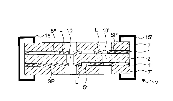
by means of known, proven chemical processes. Two thin mask foils 7, 7', e.g
25 stainless steel foils having a thickness below 100 ,um are reversibly fitted tO
the structured conductor layers 1, 1'. They are fixed by means of clips 15, 15'
and can be removed by the detachment of the latter. FL~ing is constituted by
tight pressing. The positioning of the mask foils 7, 7' takes place in known
manner, e.g. by registering bolts. Thus, to the intermediate product V and the
30 mask foils 7, 7' are applied specially shaped markings, which are e.g. made to
coincide with one another, so that ~here is a controlled positioning thereof.
2143~33
~_ P0877.PCI` - 9 -
The mask foils 7, 7' are structured by contour etching and have through ope-
nings 8, 8', which are aligned with the interfacial connection openings 4' of the
conductor layers 1, 1'. The external diameter of the through openings 8, 8' is
larger than the external diameter of the preworked interfacial connection ope-
S nings 4' of the conductor layers 1, L', but smaller than the external diameterof the pads L fitted around the preworked openings 4'. The contour etching of
the through openings 8, 8' takes place in a separate, not shown, known pro-
duction process. It is possible to use random shapes and structures, such as
round and angular openings, elongated straight and curved openings, etc. The
10 through openings 8, 8' are made larger than the preworked interfacial connec-tion openings 4', in order to compensate any dimensional changes of the pla-
stic film 2. It is advantageous to use through openings with a most favourahle
external diameter Dg for the optimum dimensioning in the case of minimum
space consumption. This is calculated from the external diameter of the pads
lS L, minus the external diameter of the preworked interfacial connection ope-
nings 4', divided by two.
The tight pressing of the mask foils 7 7' onto the intermediate product V is
made easier by the fact that the foils 7, 7' are slightly concave, so that at the
20 edges thereof they bend away slightly to the outside from the flat extension of
the intermediate product V, so that as a result of fixing by means of clips 1~,
15' bending forces are generated, ensuring a shaking-free and displacement-
free engagement of the mask foils 7, 7' on the intermediate product V for the
formation of foil packages. This is important, because the thus formed foil
25 packages must be transported, e.g. for plasma etching, into and out of the
plasma reactor.
Fig. 6 shows a foil package according to fig. S following the plasma etching of
the interfacial connection openings 10 in the plastic film 2. The openings 10
30 are etched at the position of the through opening 8, 8' of the mask film 7, 7'.
The interfacial connection openings 10 are deliberately back-etched, i.e. they
21~3~33
~_ P0877.PCr - 10-
are etched along the flat extension of the intermediate product V under the
edges of the conductor layers 1, 1' e.g. structured in the pads L or current
paths SP. Other areas of exposed plastic film 2, e.g. the insulating areas 5', are
protected against plasma action by the mask foils 7, 7'.
s
Fig. 7 shows a plasma-etched foil package according to fig. 6 following the
plating on of a contact layer 11 made from electrically conductive material,
e.g. copper. In this known, proven chemical and galvanic process the mask
foils 7, 7' and interfacial connection openings 10 of the intermediate product
10 V are coated with a contact layer 11 in such a way that the openings 10 are
plated-through. The electrically conductive material is electrochernically de-
posited and plated on. The plated-through openings 10 are referred to as
interfacial connections 12. The deposited contact layer 11 is thin and has
thicknesses below 25 ~m. The interfacial connections 12 have via connecting
areas 16, 16' electrical contact with pads L, current paths SP and mask foils 7,7'. After removal of the mask foils 7, 7' an embodiment of a two-layer foil
circuit board according to the invention is obtained.
Fig. 8 shows the two-layer foil circuit board according to fig. 7 after remo~ing20 the mask foils 7, 7'. There is no problem in removing the mask foils 7, 7' inthe case of the thin, plated on contact layers 11 with thicknesses below 10 ,um
and drawing off is possible after detaching the clips 15, 15'. For the manufac-
ture of foil circuit boards with more than two conductor layers 1, 1', e.g. sucha two-layer foil circuit board is provided with further insulator and conductor
25 layers and is photochemically and mechanically structured by repeating the
inventive method in a first variant according to figs. 1 to 8. The two-layer foil
circuit board provided with the insulator and conductor layers then once again
constitutes an intermediate product V. Structuring always takes place of those
areas of the intermediate product V which are accessible from the outside to
30 liquids, chemicals and light and on which the mask foils can be positioned.
2143~33
~_ P0877.PCI - 1 1 -
Numerous variants are available to the expert with the knowledge of the
present invention.
The thickness of the contact layers 11 is a critical parameter. With thicl;er
5 contact layers 11 there can be uncontrolled separation of the mask foils 7, 7'from the intermediate product V in the connecting area 16, 16'. This can lead
to tearing off or breaking of areas of plated on contact layers 11 and e.g. to
damage to the interfacial connections 12 by interrupting electrical contacts to
the pads L or current paths SP. Such undesired breaks due to strongly plated
10 on connections between the intermediate product V and the mask foils 7, 7'
are avoided in further variants of the process according to the invention witl
respect to figs. 9 to 27.
The mask foils 7, 7' are reutilizable resources, because, after removing the
15 plated on contact layer 11, they can be reused. In advantageous embodiments
the mask foils 7, 7' are polished metal foils, from which the plated on contact
layer 11 can be removed again by stripping. The removal of the contact layer
11 from the mask foils 7, 7' can also take place by chemical etching.
20 If any impurities, e.g. dust remain between the intermediate product V and
the mask foils 7, 7' after the fixing together thereof, then in such areas the
mask foils 7, 7' may not rest flat on the intermediate product V and small
cavities can form between them. Such cavities can be accessible during plasma
etching or also during plating on for the etching medium and respectively
25 chernicals and liquids, which is not prejudicial or can be removed in simple
manner. Firstly the etching rate in the narrow cavities is virtually zero, becau-
se only small amounts of etching medium can penetrate them. Secondly the
penetration of chemicals and liquids into such cavities during plating on can
be avoided by prior filling thereof with a harmless liquid, such as e.g. water.
2143~
P0877.PCI - 12-
Figs. 9 to 17 show a further variant of the process according to the invention
for the photochemical structuring or patterning of current paths and pads on
part of an intermediate product and mechanical structuring or patterning of
interfacial connections. The intermediate product and process steps are shown
5 in these drawings in a section along the flat extension of the intermediate
product. The process sequence for this variant largely coincides with that
described relative to figs. 1 to 8, so that reference will only be made herein-
after to the differences.
10 The main difference between the first and second variants of the process
according to the invention is that in the second variant the photoresist 3, 3' is
not stripped prior to the application of the mask foils 7, 7' and is instead left
on the intermediate product V. The process steps according to figs. 9 to 12
are consequently identical with those of figs. 1 to 4.
Fig. 13 shows the intermediate product V in the manufacturing stage accor-
ding to fig. 4 and where two thin mask foils 7, 7' have been reversibly fitted in
a direct manner to the photoresist 3, 3' by means of clips 15, 15'. The mask
foils 7, 7' have through openings 8, 8', with which the preworked interfaci~l
20 connection openings 4' can be made to coincide and have a larger diameter
than the latter.
Figs. 14 and 15 show process steps of the plasma etching and the plating on of
the further variant, which largely coincide with the corresponding process
25 steps of the variant according to figs. 6 and 7. During plasma etching the
interfacial connection openings 10 are etched and the exposed photoresist 3,
3' back-etched. These back-etched areas 14, 14' form local weak points 17, 17'
of the plated on contact layer 11 in the peel-off areas between the intermedia-
te product V and the mask foils 7, 7'. The backetchings in the photoresist 3, 3'30 are plated on in local planned manner, which on the one hand leads to good,
strong, stable connection areas 16, 16' of the interfacial connections 12 with
~1 43833
P0877.PCI' - 13-
the pads and the current paths SP and on the other local weak points 17, 17'
of the interfacial connections 12 with the mask foils 7, 7' are obtained, so that
the latter can be removed, even when applying thicker contact layers 11 with
thickness greater than 10 )lm in the vicinity of the interfacial connections 12
S without damage to the intermediate product V. This first embodiment of local
weak points 17, 17' is described in greater detail relative to fig. 26.
Figs. 16 and 17 show the intermediate product V after the removal of the
mask foils 7, 7' by releasing the clips 15, 15' and removing the mask foils 7, 7'
10 (cf. fig. 16) and after the conventional stripping of the remaining photore~ist
3, 3' (cf. fig. 17). Figs. 18 to 25 show a further variant of the process according
to the invention for the photochemical structuring or patterning of current
paths and pads on part of an intermediate product and the mechanical struc-
turing or patterning of interfacial connections with mask foils. The interme-
15 diate product and the process steps are shown in a section along the flat ex-tension of the intermediate product. The process sequence of this third variant
largely follows that of the variants described relative to figs. 1 to 8 and figs. 9
to 15, so that hereinafter only differences are explained.
20 The main difference compared with the variant of figs. 1 to 8 is that in the
third variant deposition takes place of an electrically conductive deposition
substance, e.g. a metal such as nickel or gold, as a result of chemical poten~tial
differences. The process steps according to figs. 18 to 23 are identical with
those of figs 1 to 6.
Fig. 24 shows the foil package with interfacial connections 12 in the manufac-
turing stage according to figs. 23 or 6. The difference of the chemical potenti-al between the participating conductive materials is deliberately utilized in
order to only cover the interfacial connection openings 10 in the vicinity of
30 the current paths SP and pads L, as well as the plastic film 2 with a contactlayer, so as in this way to produce interfacial connections 12. If e.g. the cur-
P0877.PCI` - 14 - 2 1 ~ 3 8 3 3
rent paths SP and pads L were structured from copper foils, then it would be
possible to chemically deposit on the intermediate product V in a nickel or
gold bath a thin nickel or gold coating. This is utilized in the process accor-
ding to the invention in order to form interfacial connections 12 in the inter-
5 facial cormection openings 10 and which are electrically contactable via con-
necting areas 16, 16' with current paths SP and pads L, without there being
strong connections to the mask foils 7, 7'.
l~is is brought about by a local, planned deposition of metal. This process is
10 controllable as a result of the chemical potential differences between the
materials used. If the mask foils 7, 7' are e.g. stainless steel foils and the de-
position substances are e.g. metal such as nickel or gold, then on the stainlesssteel foils are deposited a very small amount of nickel or gold with a thicknessof a few ~m, so that no strong connections are formed between the interme-
15 diate product V and the stainless steel foils and consequently there is nodamage to the product V on removing the stainless steel foils. If the mask
foils 7, 7' are formed by gilded, stainless steel foils, when using nickel as the
deposition substance, as a result of its favourable chernical potential differen-
ce, no nickel is deposited thereon. Nickel or gold can be very well deposited
20 on copper and in the case of corresponding activation can also be chemically
deposited on the plastic film 2. In this way foil circuit boards can be manufac-tured with plasma-etched interfacial connections 12 with diameters smaller
than 100 ~lm from deposited contact layers 11 thinner than 25 ~,lm.
25 Fig. 25 shows the intermediate product V following the removal of the mask
foils 7, 7' by detaching the clips 15, 15' and stripping the mask foils 7, 7'. As
the connections between the intermediate product V and the mask foils 7, 7'
are very thin (smaller than 10 llm) or do not exist, no damage is caused here
to the product V by breaks in the connecting areas 16, 16'.
` 2143833
P0877.PCI' - lS-
Figs. 26 and 27 show two embodiments of local weak points 17, 17' in the
peel-off area of the intermediate product V from the mask foils 7, 7'. It is
only possible to see part of the intermediate product V following the process
steps of plasma etching the through openings 10 and depositing electrically
S conductive contact layers 11.
The embodiments of local weak points 17, 17' in the peel-off area in fig. 26
shows a detailed enlargement of the variant of the process according to the
invention described relative to figs. 9 to 17, where the photoresist 3, 3' is not
10 removed or stripped after the structuring of the conductive patterns S, 5' and
interfacial connections 4, 4' prior to the application of the mask foils 7, 7' and
instead is left on the intermediate product V and where the photoresist 3, 3' isdeliberately back-etched in areas 14, 14' in the plasma etching step. The thus
back-etched areas 14, 14' form local weak points of the plated on contact
15 layer 11 in the peel-off areas between the intermediate product V and the
mask foils 7, 7'. The back-etchings in the photoresist 3, 3' are locally plated on
with metal in plarmed manner, which on the one hand leads to good, strong,
stable connecting areas 16, 16' of the interfacial connections 12 to the pads L
and the current paths SP and on the other only local weak points 17, 17' of
20 the interfacial connections 12 with the mask foils 7, 7' are formed, so that the
latter, even when applying thicker contact layers 11 with thicknesses greater
than 10 llm, can be removed in the vicinity of the interfacial connections 12
without d~m~ging the intermediate product V.
25 These local weak points 17, 17' are formed during the plating on of the back--
etched photoresist 3, 3' in the interfacial connection openings 12. Due to ~he
fact that the back-etched photoresist 3, 3' is at the end of the back-etched
areas 14, 14' (i.e. they are narrow gaps), in this process step only small
amounts of chemicals and liquids penetrate the narrow, backetched area 14,
30 14' and during the chemical and galvanic coating electrically conductive mate-
rial such as metal is preferably deposited on the conductor layers 1, 1' and the
` 2143$33
P0877.PCr - 16-
metallic mask foils 7, 7', only a small amount of metal is deposited on the
photoresist 3, 3', so that here local, thin contact layers 11 are formed and
represent local weak points 17, 17' in the critical peel-off area.
S The further embodiment of local weak points 17, 17' in the peeloff area ac-
cording to fig. 27 shows a foil circuit board manufactured according to the
variant of the process of the invention according to figs. 1 to 8 or 18 to 25. In
the second embodiment local weak points 17, 17' result from special, advanta-
geous shapes of the through openings 8, 8' of the mask foils 7, 7'. The mask
foils 7, 7' according to fig. 27 have through openings 8, 8' with shapes 20, 20',
which following the application thereof to the intermediate product V form
narrow cavities in the vicinity of the connection between the product V and
the foils 7, 7'. In these narrow cavities formed by the shapes 20, 20', electrical-
ly conductive material is deposited in locally planned manner in order in this
15 way to produce local weak points 17, 17' of the chemically and galvanically
deposited contact layer 11 in the peel-off areas between the intermediate
product V and the mask foils 7, 7'. Here again there are various possibilities
for depositing, e.g. metal. Firstly local thin contact layers 11 are formed in
said cavities, because a small amount of chemicals and liquids can penetrate
20 the said narrow cavities, so that only thin contact layers 11 form, which repre-
sent local weak points 17, 17' in the critical peel-off area. Secondly there is no
need for chemical and galvanic deposition (as in the variant according to figs.
1 to 8) and instead metal for forming the mask layers 11 can be deposited
purely chemically (as in the variant according to figs. 18 to 25). In this case, as
25 a result of the chemical potential differences between the materials used,
there is a locally planned deposition of metal. This is described in the variantaccording to figs. 18 to 25.
Figs. 28 to 32 show another variant of the process according to the invention
30 with mechanical structuring of coverings on part of a foil circuit board and
this takes in a section along the flat extension of said board.
2143833
P0877.PCI` - 17-
Fig. 28 shows a tv,~o-layer foil circuit board comprising current paths SP and
contact points K, K', insulated electrically from one another by an insulator
layer 2, arranged in two layers of electrically conductive coatings or conductorlayers 1, 1'. The two surfaces with flat extension of the foil circuit board arecalled surfaces O, O'. The current paths SP of different conductor layers 1, 1'
can be electrically contacted with one another by interfacial connections D.
The aim of the application of a structured covering is to keep the contact
points K, K' of the circuit board free from any covering, so as to be able to
subsequently load the same with components, whereas e.g. the current paths
SP and insulating surface areas of the insulating layer 2 are to be covered, so
as to protect them from mechanical damage or corrosion of metallic current J
paths.
Fig. 29 shows how it is possible to apply to the surfaces O, O' of such foil
circuit boards coverings formed from cover layers A, A' and mask foils 7, 7'
The cover layers A, A' e.g. comprise polyimide or epoxy films, as well as
epoxy resin-coated polyirnide films. The latter are e.g. used in order to con-
nect polyimide films by means of coatings of uncured epoxy resin to mask
foils 7, 7' or foil conductor boards, etc. The mask foils 7, 7' are e.g. of copper,
stainless steel, brass, bronze, aluminum-magnesium alloys, invar, molybdenum,
etc
Such epoxy resin-coated polyimide films, along their flat extension, can be
l~min~ted on one side with copper foils and on the other side can be lamina-
ted on foil circuit boards. This advantageously takes place in the same lamina-
tion process under pressure and elevated temperature. These materials are
still very flexible after the curing of the epoxy resin and are therefore general-
ly usable as coverings for flexible circuit supports.
They are inexpensive, so that the process can be inexpensively performed.
Cover layers A, A' can be simultaneously laminated onto both sides of the foil
2143~33
P0877.PCI` - 18-
circuit board, which is not possible in most of the aforementioned processes
using solder resists. The latter must be applied on one side and dried before
the second side can be treated (one exception to this is the expensive elec-
trophoretic process).
s
The interfacial connections D of the foil circuit board are filled during lami-
nation with e.g. epoxy resin-coated polyimide films, so that said conductors
are protected. The thicknesses of such copper foils and epoxy resin-coated
polyimide films are below 10 ~lm.
Fig. 30 shows the mask foils 7, 7' according to fig. 29 applied to the cover
layers A, A' and the foil circuit board following the photochemical structuring
of the foils 7, 7' in contacting structures 3, 3'. This takes place using known
photochemical processes, the contacting structures 3, 3' being transferred in
15 accordance with a photomask into the mask foils 7, 7'. The contacting structu-
res 3, 3' extend down to the cover layers A,A'. Therefore mask material-free
(copper-free) areas are formed on the cover layers A, A'. The shape of said
contacting structures 3, 3' are freely selectable and can e.g. have circular cylin-
drical, round, oval, square, rectangular or polygonal diameters.
Fig. 31 shows the mask foils 7, 7' according to fig. 30 applied to the foil circuit
board following the mechanical structuring of the cover layers A, A' in resist
openings 4, 4'. The latter are etched in a plasma etching process in the cop-
per-unprotected areas, in accordance with the contacting structures 3, 3' of the25 mask foils 7, 7'. Otherwise the mask foils 7, 7' protect the cover layers A, A'
against plasma action, so that there is no etching of the cover layers A, A' a~
this point. The edges of the contacting structures 3, 3' of the mask foils 7, 7'are back-etched and the resist openings 4, 4' have sloping walls.
30 The resist openings 4, 4' in the cover layers A, A' are plasma-etched down tothe surfaces O, O' of the foil circuit board. All these contacting structures 3, 3'
2143833
P0877.PCI' - 19-
of the mask foils 7, 7' are simultaneously etched in the plasma etching pro-
cess. Plasma etching is a known, proven process and the back-etchings and the
depth of the etchings can be precisely regulated and controlled by the expert
by means of the etching parameters such as e.g. the gas pressure, etching
5 time, etc. Plasma etching is an environmentally friendly process, which leads
to no cont~min~tion of the waste waters or sewage, which would then have to
be treated and there are no residues requiring special disposal.
As a result the contact points K, K' of the surfaces O, O' of the foil circuil
10 board are exposed, whereas e.g. the current paths SP and insulating surf ace
areas of the insulator layer 2 remain covered by the cover layers A, A'. There-
fore the aforementioned aims of said first embodiment of a structured cove-
ring for a foil circuit board are fulfilled.
15 Fig. 32 shows the f oil circuit board provided with a covering structured accor-
ding to fig. 31 after removing the mask foils 7, 7'. This can e.g. take place bywet chemical etching. In this process step naturally also exposed areas of the
foil circuit board, such as the contact points K, K' are chemically etched.
However, the mask foils 7, 7' can also be worked very thin (3 to 5 1lm thick),
20 so that they represent less than 20% of the thickness of the contact points K,
K', so that for identical etching rates of the mask materials and contact point
materials, the material loss at the contact points K, K' represents less than
20%, whilst the mask foils 7, 7' are removed. This etching away of less than
20% of the thicknesses of the exposed areas of the foil circuit board, such as
25 contact points can be accepted. This wet chemical etching is a known, proven
process and can be well controlled by the expert.
Etching rates on such exposed contact points K, K' and mask foils 7, 7' c~n
also differ. For example, the contact points K. K' can be provided with etching
30 delaying or protecting means such as thin nickel coatings or chemically depo-sited gold coatings or can entirely comprise such conductors, so that contact
21~383~
P0877.PCr - 20 -
points K, K' treated in this way during the wet etching of the mask foils 7, 7'
may be attacked by less than 20% or not at all. The application of nickel or
gold coatings to the contact points K, K' advantageously takes place prior to
the application of the covering to the foil circuit board according to fig. 29.
The structured mask foils 7, 7' do not have to be removed from the structured
cover layers A, A' and can be left thereon and used as passive electrical ele-
ments. Thus, uses as electromagnetic shielding surfaces are appropriate, e.g. toshield against high frequency radiation, which can interfere with the opera~ion
10 of the electronic circuit of the foil circuit board. With a corresponding thick-
ness of the mask foils 7, 7' the structured mask foils 7, 7' can also be used asvoltage supplies or as earth leads for the foil circuit board. The correspondingconfigurations of the thicknesses of the mask foils 7, 7', the possibly neces~arv
fitting of electrical connections between the mask foils 7, 7' and the foil circuit
15 board can all the implemented by the expert with the knowledge of the pre-
sent invention.
Fig. 33 perspectively shows part of the surface O of an exemplified embodi-
ment of a foil printed circuit board with a covering structured by the process
20 according to the invention. The foil circuit board is partly covered by the
structured cover layer A. The current paths SP are protected by e.g. a polyi-
mide layer of the cover layer A against harmful environmental influences,
whereas the contact point K is accessible in a rectangular resist opening 4,
which can be subsequently used for loading with components, for wire bon-
25 ding, etc..
Figs. 34 to 37 show another variant of the process according to the inventionwith mechanical structuring of coverings on part of a foil circuit board. Thi~
takes place in a section along the flat extension of the circuit board. The
30 process sequence of this variant largely follows the variant described relative
to figs. 28 to 32, so that only the differences will be explained hereinafter.
2143833
P0877.PCI' - 21 -
The main difference between these variants of the process of the im~ention is
that in the variant of figs. 34 to 37 the mask foils 7, 7' are not irreversibly
connected to the cover layers A, A' and instead reversibly fittable foils 7, 7'
are used. They are provided with contacting structures 3, 3' and constitute
S reutilizable resources.
Fig. 34 shows an exemplified structurable two-layer foil circuit board to he
covered, precisely as in fig. 28.
10 Fig. 35 shows how coverings comprising cover layers A, A' and mask foils 7, 7'
are applied to the surfaces O, O' of the foil circuit board. In this variant thecover layers A, A' comprise polyimide films coated with uncured epoxy resin
on only one side, e.g. along the flat extension thereof and which are irrever-
sibly connected by means of said epoxy resin to the surfaces O, O' of the
15 circuit board in a lamination process. The thicknesses of said epoxy resincoa-
ted polyimide films are below 100 ,um. However the mask foils 7, 7' are rever-
sibly connected to the cover layers A, A'. The mask foils 7, 7' are e.g. made
from stainless steel and have thicknesses below 100 ~lm. They are fixed with
holding means such as e.g. clips 15, 15' and can be removed from the mask
20 foils again e.g. by detaching the clips. Fixing consists of tight pressing. The
positioning of the mask foils 7, 7' takes place in known manner, e.g. hy regi-
stering bolts. Thus, on the foil circuit board and mask foils 7, 7' are made
specially shaped markings, which can e.g. be made to coincide, so that there is
a controlled positioning thereof. Due to the fact that the mask foils 7, 7' arc
25 removed again from the resist openings 4, 4' after plasma etching and are not,
as in the first variant, destroyed or left thereon, they constitute reutilizahleresources.
The mask foils 7, 7' are structured by contour etching and have contacting
30 structures 3, 3'. Therefore, prior to their application to the cover layers A, A',
the mask foils 7, 7' are photochemically structured in contacting structures 3,
" 2l~3833
P0877.PCI - 22 -
3'. For example, the contacting structures 3, 3' are transferred in accordancc
with a photomask to the mask foils 7, 7', after which the contacting structures
3, 3' are wet etched through the foils 7, 7', so that following the application of
the foils 7, 7' to the cover layers A, A' the structures 3, 3' form mask mate-
S rialfree areas on the coatings A, A'. It is possible to produce contacting struc-
tures 3, 3' having random shapes and structures, such as round, angular, elon-
gated straight and curved openings, etc..
Fig. 36 shows the mask foils 7, 7' according to fig. 35 applied to the foil circuit
10 board following the mechanical structuring of the cover layers A, A' in resist
openings 4, 4'. These resist openings 4, 4' are etched in a plasma etching
process in the copper-unprotected areas, in accordance with the contacting
structures 3, 3' of the mask foils 7, 7'. Otherwise the mask foils 7, 7' protectthe cover layers A, A' against plasma action, so that at this point there is no
15 etching of the coatings A, A'. The edges of the contacting structures 3, 3' of
the mask foils 7, 7' are back-etched and the resist openings 4, 4' have sloping
walls. The resist openings 4, 4' in the cover layers A, A' are plasma etched
down to the foil circuit board surfaces O, O'. As a result the contact points K,K' of the circuit board surfaces O, O' are exposed, whereas e.g. the current
20 paths SP and insulating surface areas of the insulator layer 2 remain covered by the cover layers A, A'.
Fig. 37 shows the foil circuit board provided with a covering structured accor-
ding to fig. 36 after removing the mask foils 7, 7' and the covered coil circuit25 board F structured according to the inventive process is identical with that
according to fig. 32.
The multilayer printed circuit boards and foil printed circuit boards manufac-
tured according to the process of the invention consequently have structured
30 coverings with resist openings 4, 4', which form covering material-free areason the circuit boards and foil circuit boards, said openings 4, 4' being worked
21~3833
_ P0877.PCI' - 23 -
in freely shaped manner and have circular cylindrical, round, oval, ~quare
rectangular or polygonal diameters, said openings 4, 4' forming structures with
sharply contoured edges, whose definition is smaller than 100 ,um, which are
flexible and do not chip off on bending flexible circuit carriers or supports.