Note : Les descriptions sont présentées dans la langue officielle dans laquelle elles ont été soumises.
21 4~2~ ~
' ~ ANALOG MULTIPLIER USING MULTITAIL CELL
BACKGROUND OF THE INVENTION
1. Field of the Invention
The present invention relates to a multiplier for
multiplying two analog input signals, which is to be realized
on a semiconductor integrated circuit device and more
particularly, to an analog multiplier formed of bipolar
transistors and/or metal-oxide-semiconductor field-ef~ect
transistors (MOSFETs), which can operate within an expanded
input voltage range or ranges even at a low supply voltage
such as 3 or 3.3 V.
2. Description of the Prior Art
An analog multiplier constitutes a functional circuit
block essential for analog signal applications. Recently,
semiconductor integrated circuits have been made finer and
finer and as a result, their supply voltages have been
decreasing from 5 V to 3.3 or 3 V.
Under such a circumstance, a low-voltage circuit technique
that enables to operate at such a low voltage as 3 V has
been required to be developed. In the case, the input
voltage ranges of the multiplier need to be wide as much as
possible.
The &ilbert multiplier cell is well known as a bipolar
2 4 ~
multiplier. However, the Gilbert multiplier cell has such a
structure that bipolar transistor-pairs are stacked in two
stages and as a result, it cannot respond to or cope with
such the supply voltage reduction as above. Therefore, a new
bipolar multiplier that can operate at such the low supply
voltage has been expected instead of the Gilbert multiplier
cell.
Besides, the Complementary MOS (CMOS) technology has
become recognized to be the optimum process technology for
Large Scale Integration (LSI), so that a new circuit
technique that can realize a multiplier using the CMOS
technology has been required.
To respond such the expectation as above, the inventor,
Kimura, developed multipliers as shown in Figs. 1, 4 and 7,
each of which has two squaring circuits. One o~ the squaring
circuits is applied with a differential input voltage (V1 +
V2), and the other thereof is applied with another
differential input voltage (V2 - V1), where V1 and V2 are
input signal voltages to ~e multiplied. The outputs of these
two squaring circuits are subtracted to generate an output
voltage VO~ of the multiplier, which is expressed as
VOUT = ( V1 + V2 ) 2 -- ( V2 -- V1 ) 2 = 4V1 ' V2
2~ ~2~ ~
, ~
From this equation, it is seen that the output voltage
V0~ is proportional to the product V1 v2 of the first input
voltage vl and the second input voltage V2, meaning that the
circuit having the two squaring circuits provides a
multiplier characteristic.
The squaring circuits are arranged along a straight line
transversely, not in stack, to be driven at the same supply
voltage.
The above prior-art multipliers developed by Kimura were
termed "quarter-square multipliers" since the constant "4" of
involution contained in the term of the product was changed
to "1".
Next, the Kimura's prior-art multipliers will be described
below.
First, the Kimura's prior-art multiplier shown in Fig. 1
is disclosed in the Japanese Non~ mined Patent Publication
No. 5 - 94552 (April, 1993). In Fig. 1, this multiplier
includes a first squaring circuit made of bipolar transistors
Q51, Q52, Q53 and Q54 and a second squaring circuit made of
bipolar transistors Q55, Q56, Q57 and Q58.
In the first squaring circuit, the transistors Q51 and
Q52 form a first unbalanced differential pair driven by a
first constant current source (current Io) and the
transistors Q53 and Q54 form a second unbalanced differential
21~2~
, ~
pair driven by a second constant current source (current:
Io)~ The transistor Q51 is K times in emitter area as large
as the transistor Q52 and the transistor Q54 is K times in
emitter area as large as the transistor Q53.
Emitters of the transistors Q51 and Q52 are connected in
common to the first constant current source, and emitters of
the transistors Q53 and Q54 are connected in common to the
second constant current source.
In the second squaring circuit, the transistors Q55 and
Q56 form a third unbalanced differential pair driven by a
third constant current source (current: Io) and the
transistors Q57 and Q58 form a fourth unbalanced differential
pair driven by a fourth constant current source (current:
Io)~ The transistor Q55 is K times in emitter area as large
as the transistor Q56 and the transistor Q58 is K times in
emitter area as large as the transistor Q57.
Emitters of the transistors Q55 and Q56 are connected in
common to the third constant current source, and emitters of
the transistors Q57 and Q58 are connected in common to the
fourth constant current source.
Bases of the transistors Q51 and Q53 are coupled together
to be applied with a first input voltage V~, and bases of the
transistors Q52 and Q54 are coupled together to be applied
with a second input voltage Vy~
--4--
2~2~
'.. ~
Bases of the transistors Q55 and Q57 are coupled together
to be applied with the first input voltage V~, and bases o~
the transistors Q56 and Q58 are coupled together to be
applied in opposite phase with the second input voltage VyJ
or -Vy~
The transfer characteristics and the transconductance
characteristics of the multiplier of Fig. 1 are shown in
Figs. 2 and 3, respectively, where R is e2 (~ 7.389). A
differential output current ~I shown in Fig. 2 is defined as
the difference of output currents Ip and Iq shown in Fig. 1,
or (Ip - Iq).
Fig. 2 shows the relationship between the differential
output current ~I and the first input voltage V~ with the
second input voltage Vy as a parameter. Fig. 3 shows the
relationship between the transconductance (d~I/dVs) and the
first input voltage Vs with the second input voltage Vy as a
parameter.
Second, the Kimurals prior-art multiplier shown in Fig.
4 is disclosed in the Japanese Non~ mined patent
Publication No. 4 - 34673 (February, 1992). In Fig. 4, the
multiplier includes a first squaring circuit made of MOS
transistors M51, M52, M53 and M54 and a second squaring
circuit made of MOS transistors M55, M56, M57 and M58.
In the first squaring circuit, the transistors M51 and
~4~
M52 form a first unbalanced differential pair driven by a
first constant current source (current Io)~ and the
transistors M53 and M54 form a second unbalanced differential
pair driven by a second constant current source (current:
Io)~ The transistor M52 is K' times in ratio (W/L) of a
gate-width W to a gate-length L as much as the transistor
M51, and the transistor M53 iS R' times in ratio (W/L) of a
gate-width W to a gate-length L as much as the transistor
M54.
Sources of the transistors M51 and M52 are connected in
common to the first constant current source, and sources of
the transistors M53 and M54 are connected in common to the
second constant current source.
In the second squaring circuit, the transistors M55 and
M56 form a third unbalanced differential pair driven by a
third constant current source (current: Io)r and the
transistors M57 and M58 form a fourth unbalanced differential
pair driven by a fourth constant current source (current:
Io). The transistor M56 iS R~ times in ratio (W/L) of a
gate-width W to a gate-length L as much as the transistor
M55, and the transistor M57 iS K' times in ratio (W/L) of a
gate-width W to a gate-length L as much as the transistor
M58.
Sources of the transistors M55 and M56 are connected in
2~42~ ~
common to the third constant current source, and sources of
the transistors M57 and M58 are connected in common to the
fourth constant current source.
Gates o~ the transistors MSl and MS3 are coupled together
to be applied with a first input voltage V~, and gates of the
transistors M52 and M54 are coupled together to be applied in
opposite phase with a second input voltage Vy~ or -v~.
Gates o~ the transistors MS5 and M57 are coupled together
to be applied with the first input voltage V~, and gates of
the transistors M56 and M58 are coupled together to be
applied with the second input voltage Vy~
In Fig. 4, the transconductance parameters of the
transistors M51, M54, M55 and M58 are equal to be ~, and
those of the transistors M52, M53, M56 and M57 are equal to
be K'~.
The transfer characteristics and the transconductance
characteristics of the multiplier are shown in Figs. 5 and 6,
respectively, where K' is 5. A differential output current
~I shown in Fig. 5 is defined as the difference of output
currents I+ and I- shown in Fig. 4, or (I+ - I ).
Fig. 5 shows the relationship between the differential
output current ~I and the fist input voltage V~ with the
second input voltage vy as a parameter. Fig. 6 shows the
relationship between the transconductance (d~I/dV~) and the
214~2~
first input voltage V~ with the second input voltage Vy as a
parameter.
Third, the Kimura's prior-art multiplier shown in Fig. 7
is disclosed in IEICE TRANSACTIONS ON Fu~n~M~TALsr Vol. E75-
A, No. 12, December, 1992. In Fig. 7, the multiplier
includes a first squaring circuit made of MOS transistors
M61, M62, M63 and M64 and a first constant current source
(current: Io) for driving the transistors M61, M62, M63 and
M64, and a second squaring circuit made o~ MOS transistors
M65, M66, M67 and M68 and a second constant current source
(current: Io) for driving the transistors M65, M66, M67 and
M68. The transistors M61, M62, M63, M64, M65, M66, M67 and
M68 are equal in capacity or ratio (W/L) of a gate-width W
to a gate-length L to each other.
The first and second squaring circuits are termed
"quadritail circuits" or "quadritail cells" in which four
transistors are driven by a cor~o~ constant current source,
respectively.
In the first quadritail circuit, sources of the
transistors M61, M62, M63 and M64 are connected in common to
the first constant current source. Drains of the transistors
M61 and M6~ are coupled together and drains of the
transistors M63 and M64 are coupled together. A gate of the
transistor M61 is applied with a first input voltage V~, and
2~ 2~
a gate of the transistor M62 is applied in opposite phase
with a second input voltage Vy~ or --vy. Gates of the
transistor M63 and M64 are coupled together to be applied
with the middle level of the voltage applied between the
gates of the transistors M61 and M62, or (1/2) (V~ + Vy),
which is obtained through resistors (resistance: R).
Similarly, In the second quadritail circuit, sources of
the transistors M65, M66, M67 and M68 are connected in common
to the second constant current source. Drains of the
transistors M65 and M66 are coupled together and drains of
the transistors M67 and M68 are coupled together. A gate of
the transistor M65 iS applied with the first input voltage
V,~, and a gate of the transistor M66 iS applied with the
second input voltage Vy~ Gates of the transistor M67 and M68
are coupled together to be applied with the middle level of
the voltage applied between the gates of the transistors M65
and M66, or (1/2) (V" -- Vr), which is obtained through
resistors ( resistance: R) .
Between the f irst and second quadritail circuits, the
drains coupled together of the transistors M61 and M62 and
the drains coupled together of the transistors M67 and M68
are further coupled together to form one of differential
output ends of the multiplier. The drains coupled together
of the transistors M63 and M64 and the drains coupled
2~2~3
' ~
together of the transistors M65 and M66 are further coupled
together to form the other of the differential output ends
thereof.
The transfer characteristics and the transconductance
characteristics of the multiplier are shown in Figs. 8 and 9,
respectively. A differential output current ~I shown in Fig.
8 is defined as the difference of output currents Ip and IQ
shown in Fig. 7, or (Ip - IQ) .
Fig. 8 shows the relationship between the differential
output current ~I and the first input volta~e V~ with the
second input voltage Vy as a parameter. Fig. 9 shows the
relationship between the transconductance (d~I/dVs) and the
first input voltage V~ with the second input voltage Vy as a
parameter.
Further prior-art multiplier is shown in Fig. 10, which
was developed by Wang and termed the "Wang cell". This is
disclosed in IEEE Journal of Solid-State Circuits, Vol. 26,
No. 9, September, 1991. The circuit in Fig. 10 is modified
by the inventor, Kimura, to clarify its characteristics.
In Fig. 10, the multiplier includes one quadritail
circuit made of MOS transistors M71, M72, M73 and M74 and a
constant current source (current: Io) for driving the
transistors M71, M72, M73 and M74. The transistors M71, M72,
M73 and M74 are equal in capacity (W/L) to each other.
-10-
~4
' ~
Sources of the transistors M71, M72, M73 and M74 are
connected in common to the constant current source. Drains
of the transistors M71 and M74 are coupled together to form
one of differential output ends of the multiplier, and drains
of the transistors M72 and M73 are coupled together to form
the other of the differential output ends thereof.
A gate of the transistor M71 is applied with a first
input voltage (1/2)V~ based on a reference point, and a gate
of the transistor M72 is applied in opposite phase with the
first input voltage V~, or -V~ based on the reference point.
A gate of the transistor M73 is applied with a voltage of the
half difference of the first input voltage and a second input
voltage, or (1/2)(V~ - Vy)~ A gate of the transistor M74 is
applied with the voltage (1/2)(V~ - Vy) in opposite phase,
or (-1/2)(V~ - Vy)~
The transfer characteristics and the transconductance
characteristics of the Wang's multiplier, which were obtained
through analysis by the inventor, are shown in Figs. 11 and
12, respectively. A differential output current aI shown in
Fig. 11 is defined as the difference of output currents IL
and IR shown in Fig. 10, or ( IL -IR)
Fig. 11 shows the relationship between the dif~erential
output current aI and the first input voltage V~ with the
second input voltage Vy as a parameter. Fig. 12 shows the
--11--
" ~
relationship between the transconductance (d~I/dV~) and the
first input voltage v~ with the second input voltage Vy as a
parameter.
The prior-art bipolar multiplier of Fig. 1 has input
voltage ranges that is approximately e~ual to those of the
conventional Gilbert multiplier cell. Each of the prior-art
MOS multipliers of Figs. 4, 7 and 10 has input voltage ranges
of superior linearity that is comparatively wider than those
of the Gilbert multiplier cell.
However, on operating at a low supply voltage such as 3
or 3.3 V, all of the prior-art multipliers cannot expand
their input voltage ranges of superior linearity due to
causes relating their circuit configurations.
SUMMARY OF THE INV~N-1~ION
Accordingly, an object of the present invention is to
provide a multiplier that can realize wider input voltage
ranges than those of the above prior-art ones at a low supply
voltage such as 3 or 3.3 V.
Another object of the present invention is to provide a
bipolar multiplier that can operate at a low supply voltage
such as 3 or 3.3 V.
Still another object of the present invention is to
provide an MOS multiplier that can be realized by the
2~2'~
'. ~
Complementary MOS (CMOS) process steps.
According to a first aspect of the present invention, a
two-quadrant multiplier for multiplying first and second
signals having a single multitail cell is provided.
This multiplier contains a pair of first and second
transistors having input ends and output ends, a third
transistor having an input end, and a constant current source
for driving the pair of the first and second transistors and
the third transistor.
~he first signal is applied across the input ends of the
pair, and the second signal is applied in a single phase
(i.e., a positive or negative phase) to the input end of the
third transistor.
An output signal of the multiplier as a multiplication
result of the first and second signals is derived from the
output ends of the pair.
With the multiplier according to the first aspect of the
present invention, the pair of the first and second
transistors and the third transistor are driven by the common
constant current source, and the first signal is applied
across the input ends of the pair and the second signal is
applied in a single phase to the input end of the third
transistor. Also, the multiplication result of the first and
second signals is derived from the output ends of the pair.
2 ~ ~
Therefore, the first, second and third transistors
constitute a multitail cell, and they are driven at the same
supply voltage. This means that the multiplier according to
the first aspect can operate at a low supply voltage such as
3 or 3.3 V.
Also, wider input voltage ranges than those of the prior-
art ones can be obtained.
When the first, second and third transistors are made of
bipolar transistors, a new bipolar multiplier that can
operate at a low supply voltage such as 3 or 3.3 V is
provided, instead of the Gilbert multiplier cell.
When the first, second and third transistors are made of
MOSFE~s, the multiplier can be realized by the GMOS process
steps.
The first and second transistors may be made of bipolar
transistors or MOSFETs. In the case of bipolar transistors,
bases and collectors of the bipolar transistors act as the
input ends and output ends of the pair, respectively. In the
case of MOSFETs, gates and drains of the MOSFETs act as the
input ends and output ends of the pair, respectively.
Similarly, the third transistor may be made of a bipolar
transistor or an MOSFET. In the case of a bipolar
transistor, a base of the bipolar transistor acts as the
input end of the third transistor. In the case of an MOSFET,
214~4~
a gate of the MOSFET acts as the input end of the third
transistor.
In addition, when the pair of the first and second
transistors are made of bipolar transistors, the third
transistor may be made of a bipolar transistor or an MOSFET.
Even when the pair of the first and second transistors are
made of MOSFETs, the third transistor may be made of a
bipolar transistor or an MOSFET.
Further in addition, the third transistor may be the same
in polarity as the pair of the first and second transistors,
and may be opposite in polarity to the pair. Here, the word
"polarity" means the type of a bipolar transistor, i.e., npn
and pnp, and the type of channel conductivity of an MOSFET,
i.e., n- and p-channels.
The first and second transistors forming the pair need to
be the same in polarity and in capacity (e.g., emitter area
for bipolar transistors and gate-width to gate-length ratio
W/L for MOSFETs). On the other hand, the third transistor
is optional in polarity and capacity.
In a preferred embodiment of the multiplier according to
the first aspect, the pair of the first and second
transistors and/or the third transistor are made of bipolar
transistors, and emitters of the first and second transistors
and/or an emitter of the third transistor may have resistors
2 ~
. --
or diodes for emitter degeneration purpose.
In this case, the input voltage ranges become wider than
the case of no such resistors and diodes as above.
In another embodiment of the first aspect, a dc voltage
is applied to one of the input ends of the pair, and a first
resistor is connected between the other of the input ends and
the input end of the third transistor. The second signal is
applied through a second resistor to the input end of the
third transistor. There is an additional advantage that no
differential input is required for the multiplier.
In still another preferred embodiment of the first
aspect, the first, second and third transistors are made of
bipolar transistors, and the third transistor has an emitter
area of K times as large as those of the first and second
transistors, where K = 1 or K 2 2. If the second input
signal and the thermal voltage are defined as V2 (V) and VT
(V), respectively, such a reIationship as V2 = VT- ln(4/K) is
appro~imately satisfied.
The multiplier according to the first aspect may include
at least one additional transistor. The at least one
additional transistor has an input end connected to the input
end of the third transistor and is driven by the same
constant current source.
In the case of one additional transistor, the combination
-16-
2~2~ ~
of the third and additional transistors are equivalent to one
transistor whose emitter area or gate-width to gate-length
ratio is twice as much as those of the first and second
transistors.
In general, if the multiplier contains n additional
transistors, where n > 1, the third transistor and the n
additional transistors are equivalent to one transistor whose
emitter area or gate-width to gate-length ratio is (n + 1)
times as much as those of the first and second transistors.
According to a second aspect of the present invention, a
four-quadrant multiplier for multiplying first and second
signals is provided, which contains first and second
multitail cells.
The first multitail cell contains a first pair of first
and second transistors having input ends and output ends, a
third transistor having an input end, and a first constant
current source for driving the first pair of the first and
second transistors and the third transistor.
The second multitail cell contains a second pair of
fourth and fifth transistors having input ends and output
ends, a sixth transistor having an input end, and a second
constant current source for driving the second pair of the
fourth and fifth transistors and the sixth transistor.
The output ends of the first pair are coupled with the
-17-
2~412~Q
. --
output ends of the second pair in opposite phases.
The first signal is applied across the input ends o~ the
first pair and across the input ends of the second pair in
the same phase.
The second signal is applied across the input end of the
third transistor and the input end of the sixth transistor.
In other words, the second signal is applied in a phase
(e.g., in a negative phase) to the input end of the third
transistor, and the second signal is applied in an opposite
phase (e.g., in a positive phase) to the input end of the
sixth transistor.
An output signal as a multiplication result of the first
and second signals is derived from the coupled output ends of
the first and second pairs.
With the multiplier according to the second aspect of the
present invention, the first pair of the first and second
transistors and the third transistor are driven by the first
constant current source, the second pair of the fourth and
fifth transistors and the sixth transistor are driven by the
second constant current source. The first signal is applied
across the input ends of the first pair and across those of
the second pair, and the second signal is applied across the
input ends of the third and sixth transistors. The
multiplication result of the first and second signals is
-18-
2 1 4 ~ 2 L~ ~
derived from the coupled output ends of the first and second
pairs.
Therefore, the first, second, third, fourth, fifth, and
sixth transistors are driven at the same supply voltage,
which means that the multiplier according to the second
aspect can operate at a low supply voltage such as 3 or 3.3
V.
Also, since the output ends of the first multitail cell
and those of the second multitail cell are coupled with each
other in opposite phases, the non-linearities of the transfer
characteristics of the first and second cells are cancelled
with each other, resulting in wider input voltage ranges for
good transconductance linearity than those of the conventional
ones.
Similar to the two-quadrant multiplier according to the
first aspect, when the four-quadrant multiplier according to
the second aspect is made of bipolar transistors, a new
bipolar multiplier that can operate at a low supply voltage
such as 3 or 3.3 V is provided. When the multiplier is made
of MOSFETs, it can be realized by the CMOS process steps.
As each of the first and second multitail cells, the
multiplier according to the first aspect can be employed.
In a preferred embodiment, the multiplier according to
the second aspect includes first and second compensation
--19--
2~24
'.
circuits for compensating in transconductance linearity the
first and second multitail cells. These compensation
circuits are the same in configuration.
Each of the first and second compensation circuits has a
first converter for converting an initial differential input
voltage into a differential current, and a second converter
for converting the differential current thus obtained to
produce a compensated differential input voltage that acts as
the first or second signal to be multiplied.
Preferably, the first converter is composed of a
differential pair of two transistors and two diodes connected
to differential output ends of the differential pair. The
diodes act as loads for the respective transistors. The
initial differential input voltage is applied across the
input ends of the differential pair. The compensated
differential input voltage is derived from the output ends of
the pair.
The transistors forming the differential pair of each
compensation circuit may he made of bipolar transistors or
20 MOSFETs. The diodes thereof may be made from bipolar
transistors or MOSFETs that are diode-connected.
In the present invention, the word "multitail cell" means
that a circuit cell containing three or more transistors
driven by a common constant current source, in which all
-20-
~44~4~
currents passing through the respective transistors are
defined by a constant current of the current source.
In accordance wlth the present invention, there is
provided a two-quadrant multlplier for multiplying a first
input slgnal and a second input signal, which has a single
multitail cell comprlsing:
a circuit having a differential input and a differentlal
output, said clrcuit comprising a pair of first and second
transistors;
a third transistor having an input;
a common constant current source for driving said first,
second, and third transistors, said common constant current
source being connected to said first, second and third
transistors; and
said first input signal being applied across said
differential input of sald pair of first and second
transistors, and sald second input signal being applied in a
single polarity to said input of said third transistor,
wherein an output signal from said differential output of
said pair of first and second transistors contains a
multiplication result of said first and second input signals.
In accordance with another aspect of the invention,
there is provided a four-quadrant multipller for multiplying a
first input signal and a second input signal, said multiplier
comprising:
(a) a first multitail cell;
said first multitail cell containing a first circuit
havlng a differential input and a dlfferentlal output, said
-21-
74646-16
~ 11 44 ~ 4~
flrst clrcult comprising a flrst pair of first and second
translstors;
a third translstor having an input and an output~
a first common constant current source for drlvlng sald
first palr of sald flr~t and second transistors and sald thlrd
transistor;
(b) a second multltail cell;
said second multitail cell containlng a second clrcult
havlng a dlfferentlal lnput and a dlfferentlal output, said
second clrcult comprlslng a second palr of fourth and fifth
translstors;
a sixth transistor having an input and an output;
a second common constant current source for drlving said
second pair of sald fourth and fifth translstors and sald
slxth translstor;
(c) sald dlfferential output of sald flrst palr of sald
flrst and second translstors being coupled with said
dlfferentlal output of sald second palr of fourth and flfth
transistors in opposite polaritles 7
(d) said output of sald thlrd translstor and sald output
of said sixth transistor belng coupled together;
(e) said first input signal being applied across said
differential input of said fir~t circult and across sald
dlfferentlal lnput of sald second clrcult in the same
polarlty; and
(f) sald second lnput slgnal belng applled across sald
lnput of sald thlrd transistor and sald lnput of sald sixth
transistor,
-21a-
74646-16
2 ~ O
(g) wherein an output signal from sald coupled output of
said flrst and second circults contalns a multlplication
result of said first and second lnput slgnals.
In accordance with another aspect of the inventlon,
there ls provided a two-quadrant multlplier for multiplying a
flrst lnput slgnal and a second lnput slgnal, whlch has a
single multltail cell comprising:
a clrcult havlng a dlfferential lnput and a dlfferential
output, sald clrcult comprlslng a pair of first and second
translstorss
a third translstor havlng an input;
a common constant current source for driving said first,
second, and third transistors, said common constant current
source belng connected to sald flrst, second, and thlrd
translstors~ and
sald flrst input slgnal being applled across sald
dlfferential input of said circuit, and sald second lnput
signal being applied in a slngle polarlty to sald lnput of
sald thlrd translstor,
whereln an output slgnal from sald dlfferentlal output of
sald clrcult contalns a multlpllcation result of said first
and second lnput slgnals,
whereln said flrst, second, and thlrd translstors of sald
multltail cell are blpolar transistors, sald flrst and second
transistors have equal size emltter areas and said third
transistor has an emltter area of K tlmes as large as those of
sald first and second transistors, where K ~ 1 or K ~ 2.
In accordance with another aspect of the lnventlon,
-21b-
74646-16
~ ~ ~ 4~4~
there is provided a four-quadrant multlpller for multlplylng a
first lnput signal and a second input slgnal, said multiplier
comprlsing:
(a) a first multitail cell;
said first multltail cell contalning a first circuit
havlng a dlfferentlal input and a dlfferentlal output, sald
first clrcult comprlslng a flrst palr of first and second
transistors;
a third transistor having an input and an output;
a first common constant current source for driving said
flrst pair of said first and second transistors and said third
translstor;
(b) a second multitail cell;
said second multitail cell containing a second circuit
having a differential input and a differential output, said
second clrcult comprlsing a second palr of fourth and fifth
translstors;
a sixth transistor having an input and an output;
a second common constant current source for driving said
second pair of said fourth and fifth transistors and said
sixth transistor;
(c) said differential output of sald flrst clrcuit being
coupled wlth sald dlfferential output of said second circuit
in opposite polarities 7
(d) said output of said third transistor and said output
of sald sixth translstor belng coupled together;
(e) said first input signal being applied across said
differential input of said first circuit and across said
-21c-
74646-16
~ 1 4 ~ ~ 4 ~
dlfferential lnput of said second circult ln the same
polarlty; and
(f) sald second lnput slgnal being applled across sald
input of said third translstor and said lnput of said sixth
translstor,
(g) wherein an output slgnal from sald coupled output of
said ~irst and second circuits contains a multipllcation
result of said first and second lnput slgnals,
wherein sald first and second transistors of said first
multitail cell have one of a same emitter area and gate-width
(W) to gate-length (L) ratlo (W/L), and sald third transistor
of sald first multitail cell has one of a different emitter
area and gate-width (W) to gate-length (L) ratlo (W/L) as
those of said first and second transistors, and
whereln sald fourth transistor and said fifth transistor
of sald second multitall cell have one of a same emitter area
and gate-width (W) to gate-length (L) ratio (W/L) as each
other, and said sixth transistor of sald second multitail cell
has one of a different emitter area and gatewldth (W) to gate-
length (L) ratlo (W/L) as those of sald fourth transistor andsald flfth transistor.
In accordance with another aspect of the invention,
there is provided a four-quadrant multiplier for multipl~ing a
flrst input signal and a second lnput slgnal, sald multiplier
comprising:
(a) a flrst multltail cell;
sald flrst multltail cell contalnlng a flrst clrcult
having a differentlal lnput and a dlfferential output, said
-21d-
74646-16
-
~ f 4 2 4 0
first circuit comprislng a flrst palr of first and second
translstors;
a thlrd transistor having an lnput and an output;
a flrst common constant current source for drlving sald
first pair of sald first and second transistors and said third
transistor;
(b) a second multitall cell;
sald second multltall cell containing a second clrcult
havlng a differential lnput and a dlfferentlal output, sald
second clrcuit comprising a second pair of fourth and fifth
transistors;
a sixth transistor having an input and an output;
a second common constant current source for driving said
second palr of said fourth and fifth transistors and said
sixth translstor;
(c) sald dlfferentlal output of sald first clrcult belng
coupled with said differential output of said second circuit
in opposite polarities;
(d) said output of said third transistor and said output
of sald sixth transistor being coupled together;
(e) said first lnput signal being applied across said
differentlal input of said first circuit and across said
differential input of said second clrcuit in the same
polarity; and
(f) said second input signal being applied across sald
input of said third transistor and sald input of said sixth
transistor,
(g) wherein an output signal from said coupled output of
-21e-
74646-16
~ ~ 4~Z~O
said flrst and second circuits contains a multlplication
result o~ said first and second input signals,
wherein said differential input of ~aid circuit of said
first multitail cell includes first and second terminals, a dc
voltage is applled to said first terminal of said differential
input of said circuit of sald first multitail cell, and a
first resistor is connected between said second terminal of
said dlfferential lnput and said input of sald third
translstor,
said second signal being applied through a second
resi8tor to said input of said third transistor, and
wherein said differential input of said circuit of said
~econd multitail cell lncludes thlrd and fourth terminals,
said dc voltage is applied to said third terminal of sald
differential input of said circuit of sald second multitail
cell, and a third resistor ls connected between said fourth
terminal of sald differential lnput and sald input of said
sixth transistor,
said second signal being applied through a fourth
resistor to sald input of said sixth transistor.
In accordance with another aspect of the invention,
there is provided a four-~uadrant multiplier for multiplying a
first input signal and a second input signal, said multiplier
comprislng:
(a) a first multitall cell;
said flrst multitail cell containing a first circuit
having a differential input and a dlfferential output, said
first circuit comprising a first pair of first and second
-21f-
74646-16
2 ~ 4 4 2 ~ ~
translstors;
a third transistor having an input and an output;
a first common constant current source for driving sald
first pair of said first and second transistors and said third
transistor;
(b) a second multitail cell;
said second multltail cell contalning a second clrcuit
having a differentlal input and a differential output, said
second circuit comprising a second pair of fourth and fifth
translstors;
a sixth transistor having an input and an output;
a second common constant current source for driving said
second pair of said fourth and fifth transistors and said
sixth translstor;
(c) sald differentlal output of said first circult being
coupled with said dlfferential output of said second circuit
in opposite polarities;
(d) said output of said third transistor and said output
of said sixth transistor being coupled together;
(e) said first input signal being applied across said
dlfferentlal lnput of said first circuit and across said
differential input of said second clrcult ln the same
polarity; and
(f) said second input signal being applied across said
input of said third transistor and said input of said sixth
transistor,
(g) wherein an output signal from sald coupled output of
sald flrst and second clrcults contalns a multiplication
-21g-
74646-16
2 ~ 442~
result of sald flrst and second input slgnals,
whereln said flrst, second, and thlrd translstors of said
first multltall cell are blpolar translstors, sald flrst and
second translstors have equal slze emitter areas and said
thlrd translstor has an emltter area of K times as large as
those of sald flrst and second translstors, where K c 1 or K
2,
wherein sald fourth, flfth and slxth translstors of sald
second multitail cell are bipolar transistors sald thlrd and
fourth transistors have equal size emltter areas, and sald
slxth transistor has an emltter area of K times as large as
those of said fourth and flfth translstors.
In accordance wlth another aspect of the lnventlon,
there is provlded a four-quadrant multlpller for multlplylng a
flrst lnput slgnal and a second input signal, sald multiplier
comprislng
(a) a flrst multltall cell7
said flrst multltall cell contalnlng a flrst circuit
havlng a dlfferential lnput and a differentlal output, sald
Z0 flrst circuit comprlslng a first palr of flrst and second
transistors7
a thlrd translstor havlng an lnput and an output7
a flrst common constant current source for drlvlng sald
flrst palr of sald flrst and second translstors and sald third
translstor7
(b) a second multitail cell7
said second multitail cell containing a second circuit
havlng a dlfferentlal lnput and a dlfferential output, sald
-21h-
74646-16
.
second circult comprlslng a second palr of fourth and fifth
transistors;
a sixth translstor having an lnput and an output~
a second common constant current source for drivlng sald
second palr of sald fourth and flfth transi~tors and sald
slxth translstor;
(c) sald dlfferentlal output of sald first clrcult belng
coupled wlth sald differential output of said second clrcult
in opposlte polarltles;
(d) sald output of sald thlrd transistor and said output
of sald slxth translstor belng coupled together;
(e) sald flrst lnput signal being applled across said
dlfferentlal input of sald flrst circuit and across said
dlfferential input of said second circuit in the same
polarity; and
(f) said second input slgnal belng applled across sald
lnput of sald thlrd translstor and sald lnput of sald slxth
translstor,
(g) whereln an output signal from said coupled output of
sai~ flrst and second clrcult contalns a multlplicatlon result
of sald flrst and second lnput slgnals,
said multiplier further comprlslng:
at least two additlonal translstors for sald flrst and
second multltall cells~
one of sald at least two addltional transistors having an
lnput connected to sald input of said third transistor of said
flrst multltall cell and ls drlven by sald flrst constant
current source~ and the other of sald at least two addltlonal
-211-
74646-16
, .
~ 1 44~
translstors having an lnput connected to sald lnput of sald
slxth translstor of sald second multltall cell and ls drlven
by said second constant current source.
In accordance with another aspect of the lnvention,
there i8 provided a four-quadrant multlpller for multiplylng a
flrst input slgnal and a second lnput slgnal, sald multiplier
comprlslng:
(a) a flrst multltail cellS
said flrst multltail cell contalnlng a first circuit
havlng a dlfferentlal lnput and a dlfferential output, sald
first clrcuit comprlsing a first pair of first and second
transistors;
a thlrd translstor having an input and an output;
a first common constant current source for driving said
first palr of sald flrst and second transistors and sald third
transistor7
(b) a second multltall cell;
sald second multltall cell contalnlng a second clrcult
having a dlfferentlal input and a differentlal output, sald
second clrcuit comprlslng a second pair of fourth and flfth
translstors;
a sixth transistor having an input and an output;
a second common constant current source for driving sald
second pair of said fourth and fifth transistors and said
sixth transistor;
(c) said differentlal output of sald flrst clrcult being
coupled wlth said differentlal output of said second circult
in opposite polaritles;
-21~-
74646-16
-
..
~ 1 4424~
(d) sald output of sald thlrd translstor and sald output
of sald sixth transistor being coupled together;
(e) sald first input signal being applled across sald
dlfferentlal input of sald first clrcuit and across sald
dlf~erentlal input of sald second clrcult ln the same
polarlty~ and
(f) sald second lnput slgnal being applled across sald
lnput of sald third transistor and said input of said sixth
translstor,
(g) wherein an output slgnal from said coupled output of
said first and second clrcults contalns a multlpllcatlon
result of said first and second input slgnals, and
wherein said multiplier further comprising first and
second compensation clrcuits for compensating linear transfer
characterlstlcs of said first and second multitail cells.
BRIEF DES~RIPTION OF THE DRAWINGS
Fig. 1 is a circuit diagram showing a first prior-
art multipller.
Fig. 2 is a graph showing the transfer
characterlstlc of the flrst prior-art multlplier shown in Fig.
1.
Fig. 3 ls a graph showing the transconductance
characteristlc of the flrst prior-art multiplier shown ln Flg.
1.
Fig. 4 ls a circuit diagram showlng a second prior-
art multipller.
Fig. 5 is a graph showlng the transfer
characterlstlc of the second prior-art multlpller shown ln
-21k-
74646-16
~ ~ 44 Z40
Flg. 4.
Flg. 6 ls a graph showlng the transconductance
characterlstic of the second prior-art multipller shown ln
Flg, 4,
Flg. 7 ls a circult dlagram showlng a third prlor-
art multiplier.
Flg. 8 ls a graph showlng the transfer
characteristic of the third prlor-art multlpller shown ln Flg.
7.
Fig. 9 ls a graph showlng the transconductance
characteristic of the thlrd prlor-art multlpller shown ln
f ~ -~11-
74646-16
~4~
Fig. 7.
Fig. 10 is a circuit diagram showing a fourth prior-art
multiplier.
Fig. 11 is a graph showing the transfer characteristic of
the fourth prior-art multiplier shown in Fig. 10.
Fig. 12 is a graph showing the transconductance
characteristic of the fourth prior-art multiplier shown in
Fig. 10.
Fig. 13 is a block diagram showing the basic
configuration of a multiplier according to the invention.
Fig. 14 is a circuit diagram of a multiplier containing
one multitail cell according to a first embodiment of the
invention.
Fig. 14A is a circuit diagram of a multiplier cont~;ning
one multitail cell according to a second embodiment of the
invention.
Fig. 15 is a graph showing the transfer characteristic of
the multiplier of Fig. 14 according to the first embodiment.
Fig. 16 is a graph showing the transconductance
characteristic of the multiplier of Fig. 14 according to the
first embodiment.
Fig. 17 is a circuit diagram of a multiplier containing
one multitail cell according to a third embodiment of the
invention.
'. '
Fig. 17A is a circuit diagram of a multiplier containing
one multitail cell according to a fourth embodiment of the
invention.
Fig. 18 is a graph showing the transfer characteristic of
the multiplier of Fig. 17 according to the third embodiment.
Fig. 19 lS a circuit diagram of a multiplier cont~i n i ng
one multitail cell according to a fifth embodiment of the
invention.
Fig. 20 is a graph showing the transfer characteristic of
the multiplier of Fig. 19 according to the fifth embodiment.
Fig. 21 is a graph showing the transconductance
characteristic of the multiplier of Fig. 19 according to the
fifth embodiment.
Fig. 22 is a circuit diagram of a multiplier containing
one multitail cell according to a seventh embodiment of the
invention.
Fig. 23 is a circuit diagram of a multiplier cont~;n;ng
one multitail cell according to an eighth embodiment of the
invention.
Fig. 24 is a circuit diagram of a multiplier containing
one multitail cell according to a ninth embodiment of the
invention.
Fig. 25 is a circuit diagram of a multiplier containing
one multitail cell according to a tenth embodiment of the
-23-
2 1
'.' ~
invention.
Fig. 26 is a circuit diagram of a multiplier cont~ining
one multitail cell according to a sixth embodiment of the
invention.
5Fig. 27 is a graph showing the transfer characteristic of
the multiplier of Fig. 26 according to the sixth embodiment.
Fig. 27A is a circuit diagram of a prior-art folded
Gilbert cell multiplier.
Fig. 28 is a circuit diagram of a multiplier according to
an eleventh embodiment of the invention.
Fig. 29 is a circuit diagram of a multiplier according to
a twelfth embodiment of the invention.
Fig. 30 is a circuit diagram of multiplier according to
a thirteenth embodiment of the invention.
15Fig. 31 is a circuit diagram of a multiplier cont~ining
two multitail cells according to a fourteenth embodiment of
the invention.
Fig. 32 is a circuit diagram of a multiplier according to
a fifteenth embodiment of the invention.
20Fig. 33 is a circuit diagram of a multiplier according to
a sixteenth embodiment of the invention.
Fig. 34 is a circuit diagram of a multiplier according to
a seventeenth embodiment of the invention.
Fig. 35 is a circuit diagram of multiplier according to
-24-
2~4-~2~
an eighteenth embodiment of the invention.
Fig. 35A is a circuit diagram of multiplier according to
a nineteenth embodiment of the invention.
Fig. 35B is a circuit diagram of multiplier according to
a twentieth embodiment of the invention.
Fig. 36 is a graph showing the transfer characteristic of
the multiplier of Fig. 35 according to the eighteenth
embodiment.
Fig. 37 is a graph showing the transfer characteristic o~
the multiplier of Fig. 35 according to the eighteenth
embodiment.
Fig. 38 is a graph showing the transconductance
characteristic of the multiplier of Fig. 35 according to the
eighteenth embodiment.
Fig. 39 is a graph showing the transconductance
characteristic of the multiplier of Fig. 35 according to the
eighteenth embodiment.
Fig. 40 is a circuit diagram of multiplier according to
a twenty-first embodiment of the invention.
Fig. 40A is a circuit diagram of multiplier according to
a twenty-second embodiment of the invention.
Fig. 40B is a circuit diagram of multiplier according to
a twenty-third embodiment of the invention.
Fig. 41 is a graph showing the transfer characteristic of
-2~-
2 ~ 4 ~
the multiplier of Fig. 40 according to the twenty-first
embodiment.
Fig. 42 is a graph showing the transfer characteristic of
the multiplier of Fig. 40 according to the twenty-first
embodiment.
Fig. 43 is a graph showing the transconductance
characteristic of the multiplier of Fig. 40 according to the
twenty-first embodiment.
Fig. 44 is a graph showing the transconductance
characteristic of the multiplier of Fig. 40 according to the
twenty-first embodiment.
Fig. 45 is a circuit diagram of multiplier according to
a twenty-fourth embodiment of the invention.
Fig. 46 is a graph showing the transfer characteristic of
the multiplier of Fig. 45 according to the twenty-fourth
embodiment.
Fig. 47 is a graph showing the transfer characteristic of
the multiplier of Fig. 45 according to the twenty-fourth
embodiment.
Fig. 48 is a graph showing the transconductance
characteristic of the multiplier of Fig. 45 according to the
twenty-fourth embodiment.
Fig. 49 is a graph showing the transconductance
characteristic of the multiplier of Fig. 45 according to the
-26-
2 4 ~
, --
twenty-fourth embodiment.
Fig. 50 is a circuit diagram of multiplier according to
a twenty-fifth embodiment of the invention.
Fig. 51 is a graph showing the transfer characteristic of
the multiplier of Fig. S0 according to the twenty-~ifth
embodiment.
Fig. 52 is a graph showing the transfer characteristic of
the multiplier of Fig. 50 according to the twenty-fifth
embodiment.
Fig. 53 is a graph showing the transconductance
characteristic of the multiplier of Fig. 50 according to the
twenty-fifth embodiment.
Fig. 54 is a graph showing the transconductance
characteristic of the multiplier of Fig. 50 according to the
twenty-fifth embodiment.
Fig. 55 is a circuit diagram of a bipolar compensation
circuit for the bipolar multipliers according to the
invention.
Fig. 56 is a circuit diagram of an MOS differential
circuit for the MOS multipliers according to the invention.
DETAILED DESCRIPTION OF THE PREFERRED EMBODIMENTS
Preferred embodiments o~ the present invention will be
described below referring to Figs. 13 to 56.
2 ~ ~
. --
[BASIC CONFIGURATION]
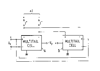
Fig. 13 is a block diagram showing the basic
configuration of a two-quadrant analog multiplier according
to the invention.
5As shown in Fig. 13, the multiplier contains a first
multitail cell A and a second multitail cell B, both of which
are the same in circuit configuration. Each of the first and
second multitail cells A and B is a circuit cell containing
three or more transistors driven by a common constant current
source, in which all currents passing through the respective
transistors are defined by a constant current of the current
source.
A first signal (voltage: V~) is applied across a first
differential input ends of the cell A and across a second
differential input ends of the cell B. A second signal
(voltage: Vy) is applied in negative phase to a first input
end of the cell A and is applied in positive phase to a
second input end of the cell B.
Differential output ends of the cell A are coupled with
differential output ends of the cell B in opposite phases,
respectively. In other words, the differential output ends
of the cell A and those of the cell B are cross-coupled.
Output currents I+ and I- forming a differential output
current ~I are derived from the cross-coupled differential
-28-
~1~4~
. --
(4)output ends of the cells A and B. The differential output
current ~I provides a multiplication result of the first and
second signals V~ and Vy~
With the multiplier shown in Fig. 13, although the first
signal V~ may be both positive and negative for the multitail
cells A and B, the second signal Vy is only positive for the
cell B and negative for the cell A. This means that this
multiplier i5 a two-quadrant one.
It has been known that a two-quadrant multiplier
generally has a comparative narrow range of satisfactorily
linear transconductance. Then, to improve the
transconductance linearity, the inventor, Kimura, has ever
developed several improved multipliers of this type by
combining a plurality of such the multipliers. The
multiplier of the present invention also is due to his
development.
This multiplier of the invention features its multitail
cells, so that the multitail cell itself is explained below
prior to the description for the combination of the multitail
cells.
The number of the transistors constituting each multitail
cell is optional if it is 3 or more. Therefore, the number
may be 5 or more; however, only a "triple-tail cell"
containing three transistors and a "quadritail cell"
-29-
2 ~ ~
containing four transistors are described here.
Fig. 13 shows the basic configuration of the multiplier
having two multitail cells; however, the invention is not
limited to the multiplier of this type, and only one of the
multitail cells A and B itself may be used as a two-quadrant
multiplier. But, the input voltage ranges are limited to
narrower than the case of two multitail cells.
[FIRST EMBODIMENT]
Fig. 14 shows a two-quadrant analog multiplier according
to a first embodiment, which is composed of only one triple-
tail cell of ~ipolar transistors.
In Fig. 14, the triple-tail cell contains a differential
pair of npn bipolar transistors Q1 and Q2, an npn bipolar
transistor Q3, and a constant current source (current: Io)~
All the transistors Q1, Q2 and Q3 have emitters connected
in common to one end of the constant current source, and they
are driven by the same current source. The other end of the
constant current source is grounded. All the transistors Q1,
Q2 and Q3 are the same in emitter area.
A supply voltage Vcc is applied to a collector of the
transistor Q3.
A first signal or a differential voltage Vl is applied
across differential input ends of the pair, i.e., bases of
the transistors Q1 and Q2. A second signal or a differential
-30-
~424Q
voltage V2 is applied in pOSitive or negative phase (or
polarity) to an input end or a base of the transistor Q3.
Then, supposing that the transistors Q1, Q2 and Q3 are
matched in characteristic and ignoring the base-width
modulation, collector currents Icl~ Ic2 and IC3 of the
respective transistors Q1, Q2 and Q3 can ~e expressed as the
following equations (1), (2) and (3), respectively.
Y.h -- VA ~ 2 V1
IC = ~Se~P ( VT (1)
VR ~ VA 2 V1
I~ = Ise~p( VT (2)
V -- V + V
In the equations (1), (2) and (3), VT is the thermal
voltage of the transistors Q1, Q2 and Q3 defined as VT = kT/q
where k is the Bolt7~nnls constant, T is absolute
temperature in degrees Kelvin and q is the charge of an
electron. Also, Is is the saturation current, VR is a dc
component of the first input voltage, and VA is a common
emitter voltage, i.e., a voltage at a connection point of the
emitters of the transistors Q1, Q2 and Q3.
Tail currents of the triple-tail cell, i.e., the
collector currents ICl, IC2 and Ic3~ satisfies the following equation.
21~2~
IC1 + IC2 + IC3 = aCFIO
where aF is the dc common-base current gain factor of the
transistors Q1, Q2 and Q3.
The commQn term Is exp{ (VR - VA)/VT} contained in the
equations (1), (2) and (3) is given as the following equation
(5) by solving the equations (1) to (4).
Is e~p( R VA ) ~Io V (5)
r { 2~( 2V ) + e~p ( r2 ) }
A differential output current ~Ic (= ICl IC2) of the
triple-tail cell is given by the follow ng equation (6).
2~F.IOsinh( 1 )
0 ~IC = IC1 - IC~Z = T (6)
{2~h( 1) + ~p( 2)}
Fig. 15 shows the transfer characteristic of the bipolar
triple-tail cell or the multiplier according to the first
embodiment, which shows the relationship between the
differential output current ~Ic and the first input voltage
V1 with the second input voltage V2 as a parameter.
It is seen from Fig. 15 that the deferential output
current ~Ic increases monotonously and has a limiting
characteristic concerning the first input voltage V1. On the
other hand, concerning the second input voltage V2, it is
seen that the current ~Ic has a limiting characteristic only
-32-
2 ~ ~
for a negative value of v2 and it varies within a very narrow
range for the negative value of V2 although the current ~Ic
increases monotonously.
The transconductance characteristics of the multiplier
according to the first embodiment can be given by
differentiating the differential output current ~Ic by the
first or second input voltage V1 or V2 in the equation (6),
resulting in the following e~uations (7) and (8).
d(~I ) I ( 2 + ~h(2V )e~p( V ))
dVl VT { 2~h(--) + e~p(--)}
d(~C) _ 2~FIO s~h(2v )e~p( V )
dV2 Vr ~2~h( - ) + e~p( V ) (8)
~ he equation (7) represents the transconductance
characteristic for the first input voltage V1, which is shown
in Fig. 16. The equation (8) represents that for the second
input voltage V2.
It is seen that the triple-tail cell, i.e., two-quadrant
analog multiplier according to the first embodiment is
expanded in linear transconductance range for the first input
voltage V1.
2 ~ ~
To make the transconductance characteristic linear for the
first input voltage V1, the second input voltage V2 needs to
satisfy the following relationship as
exp(V2/VT) = 4
~his relationship is obtained by differentiating the above
equation (6) by the voltage V1 three times and obtaining a
condition that makes a differential coefficient thus obtained
maximally flat, i.e., d3(~IC)/dVl3 = 0, at V1 = 0.
It is not always required that the second input voltage
V2 exactly satisfies such ~he relationship as exp(V2/VT~ = 4,
because such an exact value of V2 cannot be realized on a
practical semiconductor integrated circuit device.
Generally, if the transistor Q3 has an emitter area of K
times as large as those of the transistors Q1 and Q2, to make
lS the transconductance characteristic linear for the first input
voltage V1, the second input voltage V2 needs to satisfy the
following relationship as
egp(V2/VT) = 4/K, or V2 = VT- ln(4/K)
Here, since the transistor Q3 is the same in emitter area
as the transistors Q2 and Q3, the above relationship,
exp(V2/VT) = 4 is obtained.
As described above, with the triple-tail cell or
multiplier according to the first embodiment, the transistors
Q1, Q2 and Q3 are driven at the same supply voltage, which
-34-
~ 4~24~
means that this multiplier can operate at a low supply
voltage such as 3 or 3.3 V.
Also, an expanded input voltage range for good
transconductance linearity can be obtained compared with those
of the prior-art multipliers.
Further, this triple-tail cell provides a new bipolar
analog multiplier that can operate at a low supply voltage
such as 3 or 3.3 V, instead of the Gilbert multiplier cell.
[SECOND EMBODIMENT~
Fig. 14A shows a two-quadrant analog multiplier according
to a second embodiment, which is composed of only one triple-
tail cell of bipolar transistors.
~ he second embodiment is a variation of the first
embodiment as shown in Fig. 15, and is the same in circuit
configuration as the first embodiment except for the
following:
A constant dc voltage VR is applied to one of the
differential input ends of the differential pair of the
transistors Q1 and Q2, i.e., to the base of the transistor
Q2. A voltage (V1 + VR) iS applied to the other of the
differential input ends of the differential pair, i.e., to
the base of the transistor Q1; in other words, the first
input voltage Vl is applied across the differential input
ends or bases of the transistors Q1 and Q2.
-35-
2~2
-. ~
A first resistor (resistance: R) is connected between the
bases of the transistors Q1 and Q3 and a second resistor
(resistance: R) is connected to the base of the transistor
Q3.
A voltage (2V2 + V~) is applied to the base of the
transistor Q3; in other words, a voltage of twice the second
input voltage V2, or 2V2, is applied to the base of the
transistor Q3 through the second resistor. Since the first
and second resistors are the same in resistance value, a half
of the voltage 2V2, i.e., V2 is applied to the base of the
transistor Q3.
As described above, the multiplier o~ the second
embodiment is substantially the same in circuit configuration
as the first embodiment, so that it provides the same effects
or advantages as those of the first embodiment.
Also, in the first embodiment, the first input voltage V1
needs to be applied differentially across the bases of the
transistors Q1 and Q2. However, in this second embodiment,
it is not required for the voltage Vl to be differentially
applied, which is an additional advantage of the second
embodiment.
~ o be seen from the second embodiment, in general, the
same operation or function is obtained even when the same
voltage is additionally applied to the differential input
-~6-
2~4~24~
ends of the differential pair of the first and second
transistors Q1 and Q2 and the input end o~ the third
transistor Q3.
[THIRD EMBODIMENT]
Fig. 17 shows a two-quadrant analog multiplier according
to a third embodiment, which is composed of only one triple-
tail cell of MOSFETs. This is equivalent to one that the
bipolar transistors Q1, Q2 and Q3 are replaced by MOSFETs in
the first embodiment.
In Fig. 17, the triple-tail cell contains a differential
pair of n-channel MOSFETs M1 and M2, an n-channel MOSFET M3,
and a constant current source (current: Io)~
All the transistors M1, M2 and M3 have sources connected
in common to one end of the constant current source, and they
are driven by the same current source. The other end of the
constant current source is grounded. A11 the transistors M1,
M2 and M3 are the same in transconductance parameter, i.e.,
gate-width to gate-length ratio.
A supply voltage VDD iS applied to a drain of the
transistor M3.
A first signal or a differential voltage Vl is applied
across differential input ends of the pair, i.e., gates of
the transistors M1 and MZ. A second signal or a differential
voltage V2 is applied in positive or negative phase (or
21~42
'~ ~
polarity) to an input end or a gate of the transistor M3.
Then, supposing that the transistors M1, M2 and M3 are
matched in characteristic and ignoring the gate-width
modulation, drain currents ID1~ ID2 and ID3 of the respective
transistors M1, M2 and M3 can be expressed as the following
equations (9), (10) and (11), respectively.
ID1 = ~ ( VR VA + 2 V1 YT~ )
( VR VA 2 V1 2 V~)
(9)
IDI ~
2,
ID2 ~ ( VR VA -- 2 V1 -- V~ )
( VR VA + 2 V1 2 VT~ )
ID2 = ~ (10)
( VR ~ VA + 2 V1 ~ V~ )
ID3 ~ ( VR VA + V2 ~ V~ )
( VR VA + V2 2 V~l )
~D3 ~ ( 11 )
( VR VA + V2 s V~)
In the equations (9), (10) and (11), ~ is the
transconductance parameter of these MOS transistors. Here,
~ is expressed as ~(C~/2)(W/L) where ~ is the effective
carrier mobility, COx is the gate oxide capacitance per unit
-38-
~1~42~
area, and W and L are a gate-width and a gate-length of each
transistor. Also, v~ is the threshold voltage and VR is a
dc component o~ the first input voltage Vl, and VA is the
common source voltage of the transistors M1, M2 and M3.
A tail current of the triple-tail cell is expressed as
the following equation (lZ).
ID1 + ID2 + ID3 = Io (12)
A differential output current ~ID (= ID1 ~ ID2) of the
triple-tail cell is given by the following equations (13) to
(16), by solving the equations (9) to (12).
/\ ID = ID1 ID2
_ 2 ~V1Y2 + 2~V1~ 3~~ - 6V12 - 9V22
( V2 s O,IVll s ~ ~~ - 4V22, (13)
- 2V2 _ 2~ 5~ - 4V22 s ¦Vll s - 2V2 + 2 x ~ ~~ - 4V22
or
V2 2 O,lVll s -2V2 + 2~ SIo _ 4V2 )
-39-
21~2~D
~ID = ID1 ~ ID2
= { 2~ + 8 ~B ( I Vl I - 2V2)x,~ ~~ - ( I Vl I - 2V2)2 } sgn(Vl)
( lV~ 2V2, V2s ~ ~
Vl S - 5V2 - 5,~ ~~ - 4V22, - 5V2 + 5~ ~~ - 4V22 S Vl' (14)
or
5 2 5l\ ~ 2 ~
- 2V2 + 5~ ~~ - 4V22 s Vl, V22 0 )
~D ID1 ID2 = ~ V1~\ 13 -- V12
(15)
~ - 4V22 s lVll s - SV2 + ,~ ~~ - 4V22, V2 s O )
--40--
a
~D ID1 ID2 IOSgn(V1)
( 2~ - + 2V2 ~ ¦V1¦ , Or
(16)
~\ ~ - 4V22 ~ lV~ lVll, V2 ~ ~ )
Fig. 18 shows the transfer characteristic of the MOS
triple-tail cell or the multiplier according to the third
embodiment, which shows the relationship between the
differential output current ~ID and the first input voltage
V1 with the second input voltage Vz as a parameter. In Fig.
18, the input voltages V1 and V2 are normalized by (Io/~)1/2.
It is seen from Fig. 18 that the deferential output
current ~ID increases monotonously and has a limiting
characteristic concerning the first input voltage V1. On the
other hand, concerning the second input voltage V2, it is
seen that the current ~ ID has a limiting characteristic only
for a negative value of V2 and it varies within a very narrow
range for the negative value of V2 although the current ~ID
increases monotonously.
The transconductance characteristics of the multiplier can
be given by differentiating the differential output current
~ ID by the first or second input voltage V1 or V2 in the
equations (13) to (16), resulting in the following equations
(17) to (20) for V1 and the following equations (21) to (23).
~1442~D
( y ) = - 3 ~V2 ~ 2,~,~ 3~~ - 6Vl2 _ gV22
~ Vl2
'~ 3~ 6 1 9 2
( V2 ~ ~, lV~Q - 4V22 ~ (17)
- 5V2 - 5 ~ ~~ - 4V22 s ¦Vl¦ s - 25V2 + 5 x ,~ ~~ - 4V22,
or
V2 2 O, IVl¦ ~ - 2V2 + 2 SIo _ 4V2 )
dV 8 ~ { ~Vll - 2V2) = _
( V2 s 0, lVll s - 2V2 ~ Vl S - 5V2 - 5 ~\ ~~ - 4V22 ' (18)
- 5V2 ~ 5 ,~ ~~ - 4V22 S Vl ~ a~
V2 2 0, Vl s - 5V2 - 5 ,~ ~~ - 4V22, - 5V2 + 25 ,~ ~~ - 4V
--42--
~ 2 4 ~
dV = ~ ~ - Vl2 - ,~V,2
(19)
( ~ ~~ - 4V22 s lVII s - SV2 + ,~ ~~ ~ 4V22 ~ V2 s O )
d(~lD) o
( 2,~ + 2V2 s IV~ (20)
~~ - 4V22 s ¦V~ ~ s lVll, V2 s O )
'\ 3,B 6 1 9 2
( V2 s 0, lV~ ~ - 4V22 ~ (21)
- 2V2 - 2 ,~ 5 ~ - 4V22 s ¦Vl¦ s - 2V2 + 2 x ,~ ~~ - 4V2
a¢ V2 2 0, IVll s - 5V2 + 5 ,~ ~~ - 4V22 )
--43--
~ ~14~2~
d( D) = {~ Vll -2V2)2 + 1 ~ )2 } sgn(Vl)
( V2 s 0, lVll s - lV2, Vl 5 - 2V2 - 2 ~ _ - 4V22 ~ (22)
- 2V + 2 5 ~ - 4V22 s Vl, ~r
V2 2 O, Vl s - 5V2 _ 2 ,~-- - 4V22 ~ - 5V2 + 2,~_ - 4V22 s Vl )
d(~D) = o
dV2
- 4V22 s ¦Vl¦, V2 ~ ~ (23
2 ,~ ~~ + 2V2 s Vl )
--44--
2~4~2~3
It is seen that the triple-tail cell, i.e., two-quadrant
analog multiplier according to- the third embodiment is
expanded in linear transconductance range for the first input
voltage V1.
[FOURTH EMBODIMENT]
Fig. 17A shows a two-quadrant analog multiplier according
to a fourth embodiment, which is composed of only one triple-
tail cell of MOSFETs.
The fourth embodiment is a variation of the third
embodiment as shown in Fig. 17, and is the same ih circuit
configuration as the second embodiment except for the
following:
A constant dc voltage VR is applied to one of the
differential input ends of the differential pair of the
MOSFETs M1 and M2, i.e., to the gate of the MOSFE~ M2. A
voltage (V1 + VR) iS applied to the other of the differential
input ends of the differential pair, i.e., to the gate of the
MOSFET M1; in other words, the first input voltage V1 is
applied across the differential input ends or gates of the
MOSFETs M1 and M2.
A first resistor (resistance: R) is connected between the
gates of the MOSFETs M1 and M3 and a second resistor
(resistance: R) is connected to the gate of the MOSFET M3.
A voltage (2V2 + VR) is applied to the gate of the MOSFET
-45-
2~442~
M3; in other words, a voltage of twice the second input
voltage V2, or 2V2, is applied to the gate of the MOSFET M3
through the second resistor. Since the first and second
resistors are the same in resistance value, a half of the
voltage 2V2, i.e., V2 is applied to the gate of the MOSFET
M3.
As described above, the multiplier of the fourth
embodiment is substantially the same in circuit configuration
as the third embodiment (Fig. 17), so that it provides the
same effects or advantages as those of the third embodiment.
Also, in the third embodiment, the first input voltage V1
needs to be applied differentially across the gates of the
transistors M1 and M2. In this fourth embodiment, however,
it is not required for the voltage V1 to be differentially
applied. This is an additional advantage of the fourth
embodiment.
To be seen from the fourth embodiment, in general, the
same operation or function is obtained even when the same
voltage is additionally applied to the differential input
ends of the differential pair of the first and second MOSFETs
M1 and M2 and the input end of the third MOSFET M3.
[FIFTH EMBODIMENT]
Fig. 19 shows a two-quadrant analog multiplier according
to a fifth embodiment, which is composed of only one
-46-
2 ~ ~
. --
quadritail cell of bipolar transistors~
In Fig. 19, the quadritail cell contains a differential
pair of npn bipolar transistors Q1 and Q2, an npn bipolar
transistor Q3, an npn bipolar transistor 4, and a constant
current source (current: Io)~
All the transistors Q1, QZ, Q3 and Q4 have emitters
connected in common to one end of the constant current
source, and they are driven by the same current source. The
other end of the constant current source is grounded. All
the transistors Q1, QZ, Q3 and Q4 are the same in emitter
area.
Bases of the transistors Q3 and Q4 are coupled together.
Collectors of the transistors Q3 and Q4 are coupled together
to be applied with a supply voltage Vcc.
A first signal or a differential voltage Vl is applied
across differential input ends of the pair, i.e., bases of
the transistors Q1 and Q2. A second signal or a differential
voltage V2 is applied in positive or negative phase (or
polarity) to input ends or coupled bases of the transistors
Q3 and Q4.
Then, under the same condition as in the first embodimtnt
(Fig. 14), collector currents IC1' IC2~ IC3 and IC4 of the
respective transistors Q1, Q2, Q3 and Q4 can be expressed as
the following equations (24), (25) and (Z6), respectively.
-47-
2~4~2~
VR -- VA + V1
IC1 = IS~P ( 2 ) (24)
VR -- VA 2 V1
IC2=ISe~'P( VT (25)
c3 IC14 IS ~P ( R A V2 ) ( 2 6 )
In the equations (24), (25) and (26), VT iS the thermal
voltage of the transistors Q1, QZ, Q3 and Q4, Is is the
saturation current thereof, VR is a dc component o~ the first
input voltage, and VA is a common emitter voltage of the
transistors Q1, Q2, Q3 and Q4.
Tail currents of the quadritail cell, i.e., the collector
10currents Ic1l~ Ic12 IC13 and IC14 satisfies the following
equation.
Icl1 + Icl2 + Icl3 + Ic14 = aFIo (27)
where aF is the dc common-base current gain factor of the
transistors Q1, Q2, Q3 and Q4.
15The commQ~ term Is exp{ (VR - VA) /VT} contained in the
equations (24), (25) and (26) is given as the following
equation (28).
I5 ~p( R VA ) ~FIo V (28)
{2u~h(2v ) ~ e~p( V )}
-48-
2~ 2~
. ~
A differential output current ~Ic (= IC1 - Icz) of the
quadritail cell is given by the following equation 29.
2~FI~( 2V )
~c Icl -~c2 = V V (29)
{ 2~1( 1 ) + e;~p( 2 ~ }
Fig. 20 shows the transfer characteristic of the bipolar
quadritail cell or the multiplier according to the fifth
embodiment, which shows the relationship between the
differential output current ~Ic and the first input voltage
V1 with the second input voltage V2 as a parameter.
It is seen from Fig. 20 that the deferential output
current ~Ic increases monotonously and has a limiting
characteristic concerning the first input voltage Vl. On the
other hand, concerning the second input voltage V2, it is
seen that the current ~Ic has a limiting characteristic only
for a negative value of V2. This is similar to those of the
bipolar triple-tail cell according to the first embodiment
(Fig. 14).
Since the transistor Q4 is added to the bipolar triple-
tail cell of the first embodiment, the current AIc in the
fifth embodiment varies within a relatively wider range for
the negative value of V2 compared with that in the first
-49-
2 4 ~
em~odiment.
In other words, the bipolar quadritail cell of the fifth
embodiment is equivalent to a bipolar triple-tail cell
obtained by making the emitter area of the transistor Q3
twice as large as those of the transistors Q1 and Q2 in the
first embodiment.
Therefore, it is understood, in general, that the number
of additional bipolar transistor or transistors to be applied
with the second input voltage V2 may be 1, 2, 3, 4, 5, 6,
~----, and that the variation range of the differential
output current ~Ic may be expanded for the voltage V2
dependent on this number.
The transconductance characteristics of the multiplier or
bipolar quadritail cell according to the fifth embodiment is
given by differentiating the differential output current ~Ic
by the first or second input voltage v1 or V2 in the equation
(29), resulting in the following equations (30) and (31).
d~c~ aFIo(2V )e~p( V )}
2 VT VT
d~c~ aFIo~nh( 2V )e~p( V )
2 VT V~ ( 31 )
--~0 -
2 ~ ~
The equation (30) represents the transconductance
characteristic for the first input voltage Vl, which is shown
in Fig. 21. The equation (31) represents that for the second
input voltage V2.
It is seen that the quadritail cell, i.e., two-quadrant
analog multiplier according to the fifth embodiment is
expanded in linear transconductance range for the first input
voltage Vl.
To make the transconductance characteristic linear for the
first input voltage V1, the second input voltage V2 needs to
satisfy the following relationship as
exp(V2/VT) = 2
This relationship is obtained by differentiating the above
equation (29) by the voltage Vl three times and obt~in;ng a
condition that makes a differential coefficient thus obtained
maximally flat, i.e., d3(~IC)/dVl3 = 0, where V1 = 0.
This relationship is also derived from the general
relationship of exp(V2/VT) = 4/R described previously by
setting the emitter-area ratio K at 2.
It is not always required that the second input voltage
V2 exactly satisfies such the relationship as exp(V2/VT) = 2,
because such an exact value of V2 cannot be realized on a
practical semiconductor integrated circuit device.
As described above, with the quadritail cell or
-51-
~ 2l4~a
multiplier according to the fifth embodiment, the transistors
Q1, Q2, Q3 and Q4 are driven at the same supply voltage,
which means that this multiplier can operate at a low supply
voltage such as 3 or 3.3 V.
Also, an ~ n~ed input voltage range for good
transconductance linearity can be obtained compared with those
of the prior-art multipliers.
Further, this quadritail cell provides a new bipolar
analog multiplier that can operate at a low supply voltage
such as 3 or 3.3 V, instead of the Gilbert multiplier cell.
[SIXTH EMBODIMENT]
Fig. 26 shows a two-quadrant analog multiplier according
to a sixth embodiment, which is composed of only one
quadritail cell of MOSFETs. This is equivalent to one that
the bipolar transistors Q1, Q2, Q3 and Q4 are replaced by
MOSFETs in the fifth embodiment.
In Fig. 26, the quadritail cell contains a differential
pair of n-channel MOSFETs M1 and M2, an n-channel MOSFET M3,
an n-channel MOSFET M4, and a constant current source
(current: Io)~
All the MOSFETs M1, M2, M3 and M4 have sources connected
in common to one end of the constant current source, and they
are driven by the same current source. The other end of the
constant current source is grounded. All the MOSFETs M1, M2,
-52-
~14~2~
. --
M3 and M4 are the same in transconductance parameter, i.e.,
gate-width to gate-length ratio.
A supply voltage VDD is applied to coupled drains of the
MOSFETs M3 and M4.
A first signal or a differential voltage V1 is applied
across differential input ends of the pair, i.e., gates of
the MOSFETs M1 and M2. A second signal or a differential
voltage V2 is applied in positive or negative phase (or
polarity) to coupled input ends or gates of the MOSFETs M3
and M4.
Then, under the same condition as in the third embodiment
(Fig. 17), drain currents ID1 , ID2 , ID3 and ID4 of the
respective MOSFETs M1, M2, M3 and M4 are expressed as the
following equations (32), (33) and (34), respectively.
ID1 ,~ ( VR ~ VA + 2 V1 -- VT~ )
(VR VA 2 Vl 2 VT~)
(32)
ID1 = ~
(VR_VA V1 ~ VT~)
ID2 ~ ( VR -- VA -- 1 V -- V
( VR VA + 2 V1 2 VT~ )
(33)
ID2 ~
( VR -- V~l + 2 V1 VT~ )
2 ~ 4 '~
. --
ID3 ID4 = ~ ( VR -- V,~ + V2 - VT~ )2
( VR V.A + V2 ~ V~)
(34)
ID3 ID4 = ~
( VR ~ VA + V2 ~ T~)
In the equations (32), (33) and (34), ~ is the
transconductance parameter of the MOSFETs M1, M2, M3 and M4
and VA is the common source voltage of the MOSFETs M1, M2,
M3 and M4.
A tail current of the quadritail cell is expressed as the
following equation (3S).
ID1 + ID2 + ID3 + ID4 = IO
A differential output current ~ID (= ID1 - ID2) of the
quadritail cell is given by the following equations (36) to
(39), by solving the equations (32) .to (35).
~D ID1 ID2
- - ,~ VlV2 + ~Vl,~ ~~ - 2Vl2 - V22
( V2 s O,IVll s 2~ ~~ - 2V22, (36)
- 3V2 - 3~ 3I~o - 2V22 s lvll s - 3V2 + 3 X ~ 3b~ 2V22,
a~
V2 2 O, IV1l ~ -3V2 ~ 3~ 2~~ ~ 2V22 )
--54--
~D ID1 ID2
= [ 3~ + ~ { ( IVll - 2V2)2 + 2( IVll - 2V2)
x ,~ ~ ~ - 2( I Vl I - 2V2)2 } ]sgn(Vl)
( V2 s 0, IVlls - lV2, Vl ~ - 3V2 - 3~ ~~ - 8V22,
- 3V2 + 3'~ 13~ - 8V22 ~ V
or
V2 2 O, Vl ~ - 3V2 - 3,~ ~~ - 8V22,
- 3V2 + 3,~ ~~ - 8V22 ~ V1 )
~D ID1ID2 = ~ V~ 3 -- V12
(38)
~- 2V22 s lVll ~ - 3V2 + 23 x,~ 2~~ ~ 2V22, V2 s O )
~D ID1 ID2 IOSgn (V1)
+ 2V2 s IV1l ~ ~~ (39)
_ - 2V22 ~ lVll, ,~ ~~ s lVll, V2 s O )
-55-
. 2~4
' ~
Fig. 27 shows the transfer characteristic of the MOS
quadritail cell or the multiplier according to the sixth
embodiment, which shows the relationship between the
differential output current ~ID and the first input voltage
V1 with the second input voltage V2 as a parameter. In Fig.
27, the input voltages V1 and V2 are normalized by (Io/~)1/2.
It is seen from Fig. 27 that the differential output
current ~ID increases monotonously and has a limiting
characteristic concerning the first input voltage v1. On the
other hand, concerning the second input voltage V2, it is
seen that the current aID has a limiting characteristic only
for a negative value of V2.
This is similar to those of the bipolar quadritail cell
according to the fifth embodiment (Fig. 19).
Since the MOSFET M4 is added to the MOS triple-tail cell
of the third embodiment (Fig. 17), the current ~ID in the
sixth embodiment varies within a relatively wider range for
the negative value of V2 compared with that in the third
embodiment.
In other words, the MOS quadritail cell of the sixth
embodiment is equivalent to an MOS triple-tail cell obtained
by making the gate-width to gate-length ratio (W/L) of the
MOSFET M3 twice as large as those of the MOSFETs M1 and M2
in the third embodiment.
-56-
4 ~
~ herefore, similar to the bipolar case, it is understood,
in general, that the number of an additional MOSFET or
MOSFETs to be applied with the second input voltage V2 may be
1, 2, 3, 4, 5, 6, ~----, and that the variation range of the
differential output current ~ID may be expanded for the
voltage V2 dependent on this number.
The transconductance characteristics of the multiplier
according to the sixth embodiment is given by differentiating
the differential output current ~ID by the first or second
input voltage Vl or V2 in the equations (36) to (39),
resulting in the following equations (40) to (43) for V1 and
the following equations (44) to (46).
(dVD) = - ~V2 + 2~ ~~ - 2Vl2 - V22
= _ 1 ,~Vl2
'\ 1~ 2 1 2
( V2 5 ~~ ¦Vl¦ 5 2,~ ~~ - 2V22, (40)
- 3V2 - 3 ~ 2~~ - 2V22 5 IVll 5 - 2V2 + 3 x ~ 2~~ - 2V22
a~
V2 2 0,¦V1¦ 5 -3V2 + 2 ~ _ - 2V22)
21~4240
dVD) = g ,B { ~ I Vl I - 2V2 ) - 2 ,~ ~ ~ - 2( I Vl I - 2V2)2
4 ( I Vl I - 2V2)2 } sgn(Vl)
1 ~ - 2(1Vll - 2V2)2
( V2 ~ ~~ lVll ~ - 2V2 ~ Vl S - 3V2 - 3 ,~ ~~ - 8V22, (41)
~ 3V2 + 3 ,~ ~~ - 8V22 ~ V
or
V2' = O ~ Vl S - 3V2 - 3 ,~ ~~ - 8V22,
- 2V + 2 610 _ 8V22 ~ Vl )
d(~D) ~ 2Io 2 ,~ Vl2
dV~ 2Io _ V 2
,~ ~ 1 (42)
( 2 ~ ~~ - 2V2 ~ ¦Vl¦ s - 3V2 + 3 ~ 2~~ ~ 2V22, V2 ~ O )
d(~D) = o
dVl
+ 2V2 ~ lvll, or (43)
o _ 2V22 ~ ¦Vl~ Vll, V2 ~ O )
--~8--
2 4 ~
d(~D) - ~Vl - ~ vlv2
dV2 ~\ ~ 2 1 2
( V2 5 ~~ IVll 5 2~ ~~ - 2V22,
- 3V2 - 3'~ 2~~ - 2V22 5 IVll 5 - 3V2 + 3 x ,~ 2~~ - 2V22,
o~
V2 2 O, IVll ~ - 3V2 + 3 ~ 2~~ - 2V22 )
dVD = _ 2 ,B{ ( ¦Vl¦ -2V2) - 2 ,~ ~~ - 2(¦Vll - 2V2 ~2
2(1 Vl ¦ - 2V2)2 } sgn(Vl)
,~-- - 2(¦Vl¦ - 2V2)2
( V2 ~ ~~ lVll 5 - 1V2 ~ Vl < - 2V _ 2 6Io _ 8V2
(45)
- 3V2 + 3 ,~ ~~ - 8V22 ~ Vl
a~
V2 2 O, Vl ~ - 3V2 - 3 ,~ ~~ - 8V22,
- 3V2 + 23,~ 6~ _ 8V22 5 Vl )
_Ij9_
~ 2~ 2~
d(~D) = o
dV2
(~ ~~ + 2V2 s IVIj, ~ (46)
~ - 2V22 ~ lVll ~ V2 ~ ~ )
In the multiplier according to sixth embodiment, which is
made of the MOS quadritail cell, the same effects and
advantages can be obtained as those of the thid embodiment
(Fig. 17).
-60-
2 4 1~
[~V~N'l'~ EMBODIMENT]
Fig. 22 shows a two-quadrant analog multiplier according
to a seventh embodiment, which is composed of only one
triple-tail cell of two bipolar transistors and one MOSFET.
This is equivalent to one that the npn bipolar transistor Q3
is replaced by an n-channel MOSFET in the first embodiment
(Fig. 14).
In Fig. 22, this triple-tail cell contains a differential
pair of npn bipolar transistors Q1 and Q2, an n-channel
MOSFET M3 and a constant current source (current: Io)~
Emitters of the bipolar transistors Q1 and QZ and a
source of the MOSFET M3 are connected in common to one end
of the constant current source, and the bipolar transistors
Q1 and Q2 and the MOSFET M3 are driven by the same current
source. The other end of the constant current source is
grounded. The transistors Q1 and Q2 are the same in
capacity, i.e., emitter area.
A supply voltage Vcc is applied to a drain of the MOSFET
M3.
A first signal or a differential voltage V1 is applied
across bases of the transistors Q1 and Q2. A second signal
or a differential voltage V2 is applied in positive or
negative phase (or polarity) to the gate of the MOSFET M3.
In the seventh embodiment, the drain current of the
-61-
- 2~4-~4~
.. --
MOSFET M3 increases dependent on its gate voltage, the change
of which is approximately in conformity with the square-law
characteristic of an MOSFET itself.
Therefore, it is expected that the triple-tail cell of
the seventh embodiment has a transfer characteristic near
that (Fig. 15) of the first embodiment (Fig. 14).
However, since design parameters for an MOSFET are more
than those for a bipolar transistor, the input voltage range
in which the transconductance characteristic is approximately
linear for the voltage V1 can be made wider than that (about
200 mV~p) of the first embodiment
Therefore, the same effects or advantages as those in the
first embodiment can be obtained.
[ E I GHTH EMBOD IMENT ]
Fig. 23 shows a two-quadrant analog multiplier according
to an eighth embodiment, which is composed of only one
triple-tail cell of one bipolar transistor and two MOSFETs.
This is equivalent to one that the n-channel MOSFET M3 is
replaced by an npn bipolar transistor in the third embodiment
(Fig. 17).
In Fig. 23, this triple-tail cell contains a differential
pair of n-channel MOSFETs M1 and M2, an npn bipolar
transistor Q3 and a constant current source (current: Io).
Sources of the MOSFETs M1 and M2 and an emitter of the
-62-
2 ~ ~
bipolar transistor Q3 are connected in common to one end of
the constant current source, and the MOSFETS M1 and M2 and
the transistors Q3 are driven by the same current source.
The other end of the constant current source is grounded.
The MOSFETS M1 and M2 are the same in transconductance
parameter, i.e., gate-width to gate-length ratio.
A supply voltage VDD is applied to a collector of the
transistor Q3.
A first signal or a differential voltage vl is applied
across bases of the transistors Q1 and Q2. A second signal
or a differential voltage V2 is applied in positive or
negative phase (or polarity) to the gate of the MOSFET M3.
In the eighth embodiment, the collector current of the
transistor Q3 changes dependent on its base-emitter voltage,
the change of which is approximately in conformity with the
exponential characteristic of a bipolar transistor itself.
Therefore, it is expected that the triple-tail cell of
the eighth embodiment has a transfer characteristic near that
(Fig. 18) of the third embodiment (Fig. 17).
Therefore, also in the eighth embodiment, the same
effects or advantages as those in the second embodiment can
be obtained.
[NINTH EMBODIMENT]
Fig. 24 shows a two-quadrant analog multiplier according
-63-
' . 214~%~B
to a ninth embodiment, which is composed of only one triple-
tail cell of bipolar transistors. This is equivalent to one
that the npn bipolar transistor Q3 is replaced by a pnp
bipolar transistor in the first embodiment (Fig. 14).
In Fig. 24, this triple-tail cell contains a differential
pair of npn bipolar transistors Q1 and Q2, a pnp bipolar
transistor Q3 and a constant current source (current: Io)~
Emitters of the bipolar transistors Q1 and Q2 and a
collector of the transistor Q3 are connected in common to one
end of the constant current source, and the bipolar
transistors Q1, Q2 and Q3 are driven by the same current
source. The other end of the constant current source is
grounded. The transistors Q1, Q2 and Q3 are the same in
capacity, i.e., emitter area.
A supply voltage Vcc is applied to an emitter of the
transistor Q3.
A first signal or a differential voltage V1 is applied
across bases of the transistors Q1 and Q2. A second signal
or a differential voltage V2 is applied in positive or
negative phase (or polarity) to the base of the transistor
Q3.
In the ninth embodiment, if the voltage V2 is applied to
the base of the transistor Q3 with reference to the supply
voltage Vcc, similar to the first embodiment, the collector
-64-
2~4240
. --
current Ic3 of the transistor Q3 increases monotonously
dependent on the voltage V2. That is, the following
relationship is established.
IC3 = Is e~(-- 2 R VCC ~
Therefore, the substantial tail current that drives the
transistors Q1 and Q2 is expressed as
I~E = IO -- IC3 ~
so that the ninth embodiment is equivalent to a differential
pair driven by the current IEE'
The differential current ~I is given as
~I = (Io - Ic3)tanh (V1/2VT)
If two such the triple-tail cells are combined with each
other, a multiplier as shown in Fig. 27A is obtained, which
has been termed the known "folded Gilbert multiplier cell".
[TENTH EMBODIMENT]
Fig. 25 shows a two-quadrant analog multiplier according
to a tenth embodiment, which is composed of only one triple-
tail cell of MOSFETs. This is equivalent to one that the n-
channel MOSFET M3 is replaced by a p-channel MOSFET in the
third embodiment (Fig. 17).
In Fig. 25, this triple-tail cell contains a differential
pair of n-channel MOSFETs M1 and M2, a p-channel MOSFET M3
-65-
~ 2~2~
and a constant current source (current: Io).
Sources of the MOSFETs M1 and M2 and a drain of the
MOSFET M3 are connected in common to one end of the constant
current source, and the MOSFETs M1, M2 and M3 are driven by
the same current source. The other end of the constant
current source is grounded. The MOSFETs M1, M2 and M3 are
the same in transconductance parameter, i.e., gate-width to
gate-length ratio.
A supply voltage VDD is applied to a source of the MOSFET
M3.
A first signal or a differential voltage V1 is applied
across gates of the M0SFE~s M1 and M2. A second signal or
a differential voltage V2 is applied in positive or negative
phase (or polarity) to the gate of the MOSFET M3.
In the tenth embodiment, similar to the ninth embodiment,
the substantial tail current that drives the M0SFETs M1 and
M2 is expressed as
IEE = Io ID3 ~
where ID33 is a drain current of the M0SFET M3, so that the
tenth embodiment is equivalent to a differential pair driven
by the current IEE ' ~
[EL~v~Nl~ TO ~V~:N-1~N1~ EMBODIMENTS]
Figs. 28 to 34 show two-quadrant analog multipliers
according to eleventh to seventeenth em~odiments,
-66-
2~A~4~
respectively, each of which is composed of only one triple-
tail or quadritail cell of bipolar transistors.
In the above MOS triple-tail and quadritail cells, the
input voltage ranges for V1 and v2 are decided by their
capacities, i.e., gate-width to gate-length ratios (W/L) of
the MOSFETs, and therefore, the ranges can be made
comparatively wider.
On the other hand, in the above bipolar ones, the input
voltage ranges for V1 and V2 are decided by only their
emitter areas, which means that the ranges cannot be made as
wide as those of the MOS multitail cells.
To expand the input voltage ranges for the bipolar
multitail cells, additional resistors or diodes may be
provided.
The bipolar triple-tail cell according to the eleventh
embodiment is shown in Fig. 28, which has three resistors
(resistance: RE) connected to the emitters of the respective
transistors Q1, Q2 and Q3. The emitters are connected in
common to the end of the constant current source through the
resistors, respectively.
The bipolar quadritail cell according to the twelfth
embodiment is shown in Fig. 29, which has four resistors
(resistances: RE) connected to the emitters of the respective
transistors Q1, Q2, Q3 and Q4. The emitters are connected
-67-
~14~24~
in common to the end of the constant current source through
the resistors, respectively.
The bipolar triple-tail cell according to the thirteenth
embodiment is shown in Fig. 30, which has first and second
resistors whose resistance values are RE1 and RE2 ~
respectively. The first resistor (RE1) is connected to the
coupled emitters of the transistors Q1 and Q2. The second
resistor (RE2) is connected to the emitter of the transistor
Q3.
The coupled emitters of the transistors Q1 and Q2 are
connected in common to the end of the constant current source
through the first resistor. The emitter of the transistor Q3
is connected to the end of the constant current source
through the second resistor.
The bipolar quadritail cell according to the fourteenth
embodiment is shown in Fig. 31, which has first and second
resistors whose resistances are RE1 and RE2, respectively.
The first resistor (RE1) is connected to the coupled emitters
of the transistors Q1 and Q2. The second resistor (REZ) is
connected to the coupled emitters of the transistors Q3 and
Q4.
The coupled emitters of the transistors Q1 and Q2 are
connected in common to the end of the constant current source
through the first resistor. The couple emitters of the
-68-
2 4 ~
--
transistors Q3 and Q4 are connected to the end of the
constant current source through the second resistor.
The bipolar quadritail cell according to the fifteenth
embodiment is shown in Fig. 32, which has first and second
resistors whose resistances are both RE . The first resistor
is connected to the coupled emitters of the transistors Q1
and Q3. The second resistor is connected to the coupled
emitters of the transistors Q2 and Q4.
The coupled emitters of the transistors Q1 and Q3 are
connected in common to the end of the constant current source
through the first resistor. The coupled emitters of the
transistors Q2 and Q4 are connected to the end of the
constant current source through the second resistor.
In the above eleventh to fifteenth embodiments, the
emitter resistors are arranged in the form of T character;
however, it is needless to say that they may be arranged in
the form of ~ character or the like.
Such the method of adding the emitter resistors is termed
the "emitter degeneration method". In this method, the
input voltage ranges for V1 and V2 of a bipolar multitail
cell can be enlarged if the degeneration value is set optimum
for each emitter resistor, where the degeneration value is
defined as the product of each emitter resistance value and
the tail current value, because of improvement in
-69-
21~2~
transconductance linearity.
The bipolar triple-tail cell according to the sixteenth
embodiment shown in Fig. 33 has series-connected diodes Dll
connected to the emitter of the transistor Q1, series-
connected diodes D2l connected to the emitter of thetransistor QZ, and series-connected diodes D31 connected to
the emitter of the transistor Q3. The emitters of the
transistors Q1, Q2 and Q3 are connected in common to the end
of the constant current source through the diodes D11, D21 and
D31, respectively.
The bipolar triple-tail cell according to the seventeenth
embodiment is shown in Fig. 34, which has series-connected
diodes Dl1 connected to the emitter of the transistor Q1,
series-connected diodes D21 connected to the emitter of the
transistor Q2, series-connected diodes D31 connected to the
emitter of the transistor Q3, and series-connected diodes D
connected to the emitter of the transistor Q4. The emitters
are connected in common to the end of the constant current
source through the diodes Dl1, D2l, D3l and D4l, respectively.
In the sixteenth and seventeenth embodiments, the input
voltages Vl and V2 are divided by the corresponding diodes to
be applied to each transistors.
Also, if the number of each of series-connected diodes is
defined as n, although the necessary supply voltage, i.e.,
-70-
2 4 ~
the operating voltage for each multitail cell increases by
n-VBE where the base-emitter voltage of each transistor;
however, the obt~;n~hle input voltage ranges can be expanded
to (n + 1) times the ranges shown in Fig. 15 or 20.
For example, if n = 1, the input voltage ranges are
expanded to twice the ranges in Fig. 15 or 20, and at the
same time, the operating voltage increases by 0.7 V.
However, compared with the conventional Gilbert multiplier
cell, the supply voltage can be reduced because the input
voltage ranges for Vl and V2 need not be set separately or
differently.
Therefore, in the case of the emitter diodes, the
multitail cells according to the sixteenth and seventeenth
embodiments can operate at a low supply voltage such as 3 or
3.3 V together with the enlarged input voltage ranges.
The above methods of adding the emitter resistors or
diodes may be also applied to the case of three or more
transistors to be applied with the second voltage Vl.
[EI (~H'1 ~:~:N~1~ EMBODIMENT]
In the above first to seventeenth embodiments, one
triple-tail or quadritail cell is employed; however, a
multiplier can be obtained by using two such the triple-tail
or quadritail cells.
Fig. 35 shows a four-quadrant analog multiplier according
2~ ~2~
. --
to an eighteenth embodiment, which is composed of two triple-
tail cells of bipolar transistors. This is equivalent to one
that the triple-tail cells according to the first embodiment
shown in Fig. 14 are combined with each other.
In Fig. 35, this multiplier comprises first and second
bipolar triple-tail cells.
The first triple-tail cell contains a differential pair
of npn bipolar transistors Q11 and Q12, an npn bipolar
transistor Q13 and a first constant current source (current:
Io)
The transistors Q1~, Q12 and Q13 have emitters connected
in common to one end of the first constant current source,
and they are driven by the same current source. The other
end of the first constant current source is grounded.
The transistors Q11, Q12 and Q13 are the same in emitter
area.
A first load resistor (resistance: RL) is connected to a
collector of the transistor Q11 and a second load resistor
(resistance: RL) is connected to a collector of the
transistor Q12. A supply voltage Vcc is applied to the
collectors of the transistors Q11 and Q12 through the first
and second resistors, respectively. The supply voltage Vcc
is directly applied to a collector of the transistor Q13.
A first signal or a differential voltage V~ is applied
~ ~ 4 ~
. --
across differential input ends of the pair, i.e., ba~es of
the transistors Q11 and Q12. A second signal or a
differential voltage Vy is applied in negative phase or
polarity to an input end or a base of the transistor Q13.
The second triple-tail cell contains a differential pair
of npn bipolar transistors Q14 and Q15, an npn bipolar
transistor Q16 and a second constant current source (current:
Io).
The transistors Q14, Q15 and Q16 have emitters connected
in common to one end of the second constant current source,
and they are driven by the same current source. The other
end of the second constant current source is grounded.
The transistors Q14, Q15 and Q16 are t~e same in emitter
area.
The first load resistor is connected to a collector of
the transistor Q15 and the second load resistor is connected
to a collector of the transistor Q14. The supply voltage Vcc
is applied to the collectors of the transistors Q15 and Q14
through the first and second resistors, respectively. The
supply voltage Vcc is directly applied to a collector of the
transistor Q16.
The first signal or the differential voltage V~ is
applied across differential input ends of the pair, i . e .,
bases of the transistors Q14 and Q15. The second signal or
-73-
2 4 ~
. --
the differential voltage Vy is applied in positive phase or
polarity to an input end or a base of the transistor Q16.
The voltage V~ is applied to the bases of the transistors
Q 11 and Q 14 in positive phase and to the bases of the
S transistors Q12 and Q15 in negative phase.
The coupled collectors of the transistors Q11 and Q15 are
coupled with the coupled collectors of the transistors Q12
and Q14 in opposite phases, constituting a differential
output ends of the multiplier, to which the first and second
load resistors are connected, respectively.
Then, similar to the first em~odiment, supposing that the
transistors Q11, Q12, Q13, Q14, Q15 and Q16 are matched in
characteristic and ignoring the base-width modulation, an
output differential current ~IB of this multiplier can be
given by the following equation (47).
In the equation (47)~ Ic1l~ IC12' Ic13 and IC14 are collec
currents of the transistors Q11, Q12, Q13 and Q14,
respectively, and IB~ and IB- are output currents from the
coupled collectors of the transistors Q11 and Q13 and from
those of the transistors Q12 and Q14, respectively.
~B IB IB ( IC11 IC13 ) ( IC12 + IC14 )
VX V
4~FIOSinh~ 2V ) ( 2YT (47)
{2x~h(2v ) + e~p(2V )}{2~h(2V ) + e~p(-2Y )I
-74-
2 ~ a
Figs. 36 and 37 show the transfer characteristics of the
multiplier according to the eighteenth embodiment. Fig. 36
shows the relationship between the differential output current
~IB and the first input voltage V~ with the second input
S voltage Vy as a parameter. Fig. 37 shows the relationship
between the differential output current ~IB and the second
input voltage vy with the first input voltage V~ as a
parameter.
It is seen from Figs. 36 and 37 that the deferential
output current ~ IB has a limiting characteristic for the
first input voltage V~, and on the other hand, the current
~ IB has a limiting characteristic for the second input
voltage Vy~
The transconductance characteristics of the multiplier can
be given by differentiating the differential output current
~IB by the first or second input voltage V~ or Vy in the
equation (47), resulting in the following equation (48) and
Fig. 38 for V~ and the following equation (49) and Fig. 39
for Vy~
-75-
~. ~ 2 ~ ~
d( ~IB) 2cl:FIo
dVx VT
cosh( x ) nh(
x [
VT 2VT V ( 2V ) + e~ Y ) } ( 48 )
4~2( 2 )~h( Y ) { 2CO~h(--) + CO~h( Y ) }
V V 2 V V 2
d(~IB) 2 ~F~O
dVy VT
X [ si~ (~ 2 V )CO~( 2 Y
2VT 2VT ~~h( 2V ) + ~;P(----) }
4s~ih( VX )si~h2( VY )
{ 2CO~( 2V ) + e~q?( 2V ) } { 2C~( 2V ) + e~p( 2V ) }
-76-
21 ~ !~ 2 ~ ~
. --
It is seen that the four-quadrant analog multiplier
according to the eighteenth embodiment is expanded in linear
transconductance range for the first input voltage v1.
[N lN~S'l~;~;N '1~1 ~MBOD IM13NT ]
Fig. 35A shows a four-quadrant analog multiplier according
to a nineteenth embodiment, which is composed of two triple-
tail cells of bipolar transistors. This is equivalent to one
that the triple-tail cells according to the second embodiment
shown in Fig. 14A are combined with each other.
It is also said that this multiplier is the same in
configuration as that of the eighteenth embodiment shown in
Fig. 35 other than that four resistors and a dc voltage
source are added.
In Fig. 35A, a constant dc voltage VR is applied to the
bases of the transistors Q12 and Q14. A first voltage V1,
which is not a differential one, is applied to the base of
the transistors Q11 and Q15.
A first resistor (resistance: R) is connected between the
bases of the transistors Q11 and Q13 and a second resistor
(resistance: R) is connected to the base of the transistor
Q13. A third resistor (resistance: R) is connected between
the bases of the transistors Q15 and Q16 and a fourth
resistor (resistance: R) is connected to the base of the
transistor Q16.
-77-
2 ~ ~
A voltage (V~/2) is applied to the bases of the
transistors Qll, Q12, Q13, Q14, Q15 and Q16, so that the
voltage Vl need not be a differential one.
The voltage V2 is divided by the first and second
resistors to be applied to the base of the transistor Q13 on
the one hand, and it is divided by the third and fourth
resistors to be applied to the base of the transistor Q16,
on the other hand.
Therefore, the output value of the multiplier becomes a
half that of the eighteenth embodiment.
[TWENTIETH EMBODIMENT]
Fig. 35B shows a four-quadrant analog multiplier according
to a twentieth embodiment, which is composed of two triple-
tail cells of bipolar transistors. This also is equivalent
to one that the triple-tail cells according to the second
embodiment shown in Fig. 14A are combined with each other.
It is also said that this multiplier is the same in
configuration as that of the eighteenth embodiment shown in
Fig. 35 other than that eleven resistors and a dc voltage
source are added.
In Fig. 35B, a first resistor (resistance: R) is
connected between the base of the transistor Qll and an input
end for the voltage Vx, and a second resistor (resistance: R)
is connected between the bases of the transistors Qll and
-78-
~144~4~
Q12. A third resistor (resistance: R) is connected between
the input end for the voltage V~ and the base of the
transistor Q13, and a fourth resistor (resistance: R) is
connected between the base of the transistor Q13 and an input
end for the voltage Vy~
A fifth resistor (resistance: R) is connected between the
base of the transistor Q15 and the input end for the voltage
Vy~ and a sixth resistor (resistance: R) is connected between
the base of the transistors Q15 and the input end for V~.
A seventh resistor (resistance: R) is connected between the
input end for the voltage Vy and the base of the transistor
- Q16, and an eighth resistor (resistance: R/2) is connected
between the bases of the transistors Q16 and Q12.
A ninth resistor (resistance: R) is connected between the
bases of the transistors Q11 and Q14, and a tenth resistor
(resistance: R) is connected between the base of the
transistors Q14 and the input end for the voltage Vy~
A constant dc voltage V~ is applied to the base of the
transistor Q11 through the first resistor, is applied
directly to the base of the transistor Q 12, and is applied
to the base of the transistor Q13 through the fourth, ninth
and tenth resistors.
The constant dc voltage V~ is also applied to the base of
the transistor Q14 through the ninth resistor, and is applied
-78-
2 ~ ~
to the base of the transistor Q16 through the eighth
resistor.
With this multiplier, a voltage (V~/2) is applied to the
~ases of the transistors Q11, Q12 and Q13 forming the first
triple-tail cell, and a voltage [(V~/Z) + V~] is applied to
the bases of the transistors Q14, Q15 and Q16 forming the
second triple-tail cell.
There is an advantage that both the input voltages Vl and
V2 need not be differential ones. However, the output value
of the multiplier becomes a quarter that of the eighteenth
embodiment.
[TWENTY-FIRST EMBODIMENT]
Fig. 40 shows a four-quadrant analog multiplier according
to a twenty-first embodiment, which is composed of two
triple-tail cells of MOSFETs. This is eq~ivalent to one that
the triple-tail cells according to the third embodiment shown
in Fig. 17 are combined with each other.
In Fig. 40, this multiplier comprises first and second
MOS triple-tail cells.
The first triple-tail cell contains a differential pair
of n-channel MOSFETs M11 and M12, an n-channel MOSFET M13 and
a first constant current source (current: Io)~
The MOSFETs M11, M12 and M13 have sources connected in
common to one end of the first constant current source, and
-80-
21~2~
they are driven by the same current source. The other end
of the first constant current source is grounded.
The transistors M11, M12 and M13 are the same in gate-
width to gate-length ratio.
A first load resistor (not shown) is connected to a drain
of the MOSFET M11 and a second load resistor (not shown) is
connected to a drain of the MOSFET M12. A supply voltage VDD
is applied to the drains of the MOSFETs M11 and M12 through
the first and second resistors, respectively. The supply
voltage VDD is directly applied to a drain of the MOSFET M13.
A first signal or a differential voltage V~ is applied
across differential input ends of the pair, i.e., gates of
the MOSFETs M11 and M12. A second signal or a differential
voltage Vy is applied in negative phase or polarity to an
input end or a gate of the MOSFET M13.
The second triple-tail cell contains a differential pair
of n-channel MOSFETs M14 and M15, an n-channel MOSFET M16 and
a second constant current source (current: Io)~
The MOSFETs M14, M15 and M16 have sources connected in
common to one end of the second constant current source, and
they are driven by the same current source. The other end
of the second constant current source is grounded.
The MOSFETs M14, M15 and M16 are the same in gate-width
to gate-length ratio.
-81-
2 ~
The first load resistor is connected to a drain of~ the
MOSFET M15 and the second load resistor is connected to a
drain of the MOSFET M14. The supply voltage VDD is applied
to the drains of the MOSFETS M15 and M14 through the f irst
and second res istors, respectively . The supply voltage VDD
is directly applied to a drain of the MOSFET M16.
The first signal or the differential voltage V" is
applied across differential input ends of the pair, i . e .,
gates of the MOSFETS M14 and M15. The second signal or the
differential voltage Vy is applied in positive phase or
polarity to an input end or a gate of the MOSFET M16.
The voltage V" is applied to the gates of the MOSFETS M11
and M14 in positive phase and to the gates of the MOSFETS M12
and M15 in negative phase.
The coupled drains of the MOSFETS M11 and M15 are coupled
with the coupled drains of the MOSFETS M12 and M14 in
opposite phases, constituting a differential output ends of
the multiplier, to which the first and second load resistors
are connected, respectively.
Then, similar to the third em~odiment, supposing that the
MOSFETS M11, M12, M13, M14, M15 and M16 are matched in
characteristic and ignoring the gate-width modulation, an
output differential current ~IM of this multiplier can be
given by the following equations (50), (51), (52) and ~53)-
--82-
2~42~
. --
In these equations, ID11~ IDlz, ID13 and ID14 are drain
currents of the MOSFETs M11, M12, M13 and M14, respectively,
and IM+ and IM- are output currents f rom the coupled drains of
the MOSFETS M11 and M13 and from those of the MOSFETS M12 and
S M14, respectively.
~M IM IM ( ID11 ID13 ) (ID12 ID1~) 3 13 VXVY
(IVXI 5 5 5~ ~ VY ,IVXIS ~ ~ VY )
~M = IM -- IM = ( ID11 + ID13 ) (ID12 + ID1~
= l~vy _ 1{ ,~V,~-- - 3vX2 _ 2Vy2 }sgn(Vy)
+{ 2~ + 8~(¦VX¦ + IVYI)X~ ~~ -(¦VS¦+¦VY¦)2 ~sgn(VxVy) (51)
(IVXI 2 ~ - - V2 ,IV I S IVYI + 2 SIO V2 )
~M = IM ~ IM = ( IDI1 + ID13 ) ( IDI2 + ID14 )
= 1~V Y -{ 1 ~V ~ - -3VX2- 1V~?- ~VX~ ~~- VX2}5
(52)
I VY I 2 5Io _ V 2,lVXI 5 ~ ~ - VY )
--83--
2 1 ~
>
= IM ~ IM = (ID11 + ID13 ) ( ID12 ID14 )
={ 2~+ 8~(lV~I+IVyl)x ~ ~0-(IV~l+lVyl)2}sgn(VxV~
Vx~ ~ ~ Vy2 ~ lVxl )
Figs. 41 and 42 show the transfer characteristics of the
multiplier according to the twenty-first embodiment, in which
the input voltages V~ and Vy are normalized by (Io/~)}1/2,
. Fig. 41 shows the relationship between the differential
output current ~IM and the first input voltage V~ with the
second input voltage Vy as a parameter. Fig. 42 shows the
relationship between the differential output current ~IM and
the second input voltage Vy with the first input voltage V~
as a parameter.
It is seen from Figs. 41 and 42 that, if each of the
MOSFETs M11, M12, M13, M14, M15 and M16 has an square-law
characteristic, the deferential output current ~IM has an
ideal multiplication characteristic for the first and second
lS input voltages V~ and Vy within the ranges of V~ and Vy in
which none of the MOSFE~s M11, M12, M13, M14, M15 and M16
occurs the pinch-off phenomenon. Also, it is seen that as
the voltages V~ and Vy increase, the pinch-off phenomenon
begins to occur so that the transfer characteristics for V~
and Vy deviate from the ideal multiplication characteristics,
-84-
2~4~24~
respectively.
With the multiplier according to the twenty-first
embodiment, the input voltage ranges that provide the ideal
multiplication characteristics are particularly wide.
Especially, the input voltage range is extremely wide for the
second input voltage Vy~ being beyond +(Io/~)}1/2. This means
that the input voltage ranges for V~ and Vy are greatly
expanded or improved.
The transconductance characteristics of the multiplier is
given by differentiating the differential output current ~IM
by the first or second input voltage V~ or Vy in the
equations (50) to (53), resulting in the following equations
(54) to (57) and Fig. 43 for V~ and the following equations
(58) to (61) and Fig. 44 for V
d(~M) _ 2~V
__
lS (54)
( IV I ~ IVYI + 2~ 2Io _ Vy2,lVxl 5 ~ ~~ - Vy2)
--85--
M = _ E~ V - { ~ 1 _ _ 3 V2 _ 1 V2 _ 1 ~ Vxl Vxl
dVX 3 3 ~ ,B 2 2 2 3Io 3 V 2 1 V 2
+ 8 ~ \ ~~ - ( I Vxl + I v 1)2 _ 1 ~(1 Vxl + I vy 1)2
,~ ~~ - (I VXI + I Vyl)2
( lVXI 2 ,~ ~~ - Vy2, lV I ~; _ lVyl + 2 SIo 2
d u)( = 3 ~Vy -{ ~ 3~ ~ - 2VX - 2VY - 2
2 Vx - 2 Vy2
_~ 2Io- V2 + ~Vxl xl }sgn(Vy) (56)
o _ V2
yl 2 SIo _ v2, lVXI s,~ ~~ - vy )
-86-
2 ~ ~
d(~) 1 { ,~ 8Io _ ~ lV I + IVyl )2
,~( lvXI + lvyl)2 } (V)
o -(IVl + IVI)2 (57)
S ¦VXI ~ Vy2 S lVXI )
d(~M) 213 V
( lVxl s _ I Yl + 2 ,,~ _ _ V2, lV I ~; 2Io _ V2 ~ (58)
d(~M) = 1 ~V + 1 ~vxlvyl
dVy 3Io - 3 V 2 - 1 V 2
'\ ,~ 2 x 2 Y
+ 1 { ~ '~ - ( l V~I + l Vy l )2
I xl I ,1 ) } sgn(Vx)
~~ ~ ( lVxl + lvyl )2
( lVxl 2 ,~ ~~ - Vy2, lV I ~; _ lVyl + 2 SIo 2
-87-
.~ 2~24a
d(~M) = 1 13V ~ 1 ~vxlvyl
dVy 3Io - 3V2 - lV2
2 x 2 Y
(60)
(lVI 2 _ IVYI + 2 ,~ _ - VY2, IVXI ~ ~ ~~ - VY2 )
~V 8 { ~ ~~ - ( I VXI + I V 1)2 13(1 VXI + I VY1)2
~ ~~-(IVxl+lVyl)2 (61)
( ~ Io ~ lVxl ~ ~ _ ~ Vy2 ~ lVxl )
It is seen from Figs. 43 and 44 that the four-quadrant
analog multiplier according to the twenty-first embodiment has
a particularly wide linear-transconductance range for the
first and second input voltages V~ and Vr.
[lw~N~lY-SECOND EMBODIMENT]
Fig. 40A shows a four-quadrant analog multiplier according
to a twenty-second embodiment, which is composed of two
triple-tail cells of MOSFETs. This is equivalent to one that
the triple-tail cells according to the fourth embodiment
shown in Fig. 17A are combined with each other.
It is also said that this multiplier is the same in
-88-
2~42~
. --
configuration as that of the nineteenth embodiment shown in
Fig. 40 other than that four resistors and a dc voltage
source are added.
In Fig. 40A, a constant dc voltage VR is applied to the
gates of the MOSFETs M12 and M14. A first input voltage V~,
which is not a differential one, is applied to the gate of
the MOSFETs M11 and M15.
A first resistor (resistance: R) is connected between the
gates of the MOSFETs M11 and M13 and a second resistor
(resistance: R) is connected to the gate of the MOSFET M13.
A third resistor (resistance: R) is connected between the
gates of the MOSFETs M15 and M16 and a fourth resistor
(resistance: R) is connected to the gate of the MOSFETs M16.
A voltage (V~/2) is applied to the gates of the MOSFETs
M11, M12, M13, M14, M15 and M16, so that the voltage Vl need
not be a differential one.
The voltage V2 is divided by the first and second
resistors to be applied to the gate of the MOSFET M13 on the
one hand, and it is divided by the third and fourth resistors
to be applied to the gate of the MOSFET M16, on the other
hand.
Therefore, the output value of the multiplier becomes a
half that of the twenty-first em~odiment.
[TWENTY-THIRD EMBODIMENT]
-89-
2~ 2~0
Fig. 40B shows a four-quadrant analog multiplier according
to a twenty-third embodiment, which is composed of two
triple-tail cells of MOSFETs. This also is equivalent to one
that the triple-tail cells according to the fourth embodiment
shown in Fig. 17A are combined with each other.
It is also said that this multiplier is the same in
configuration as that of the twenty-first embodiment shown in
Fig. 40 other than that eleven resistors and a dc voltage
source are added.
In Fig. 40B, a first resistor (resistance: R) is
connected between the gate of the MOSFETs M11 and an input
end for the voltage V~, and a second resistor (resistance: R)
is connected between the gates o~ the MOSFETs M11 and M12.
A third resistor (resistance: R) is connected between the
input end for the voltage V~ and the gate of the MOSFET M13,
and a fourth resistor (resistance: R) is connected between
the gate of the MOSFETs M13 and an input end for the voltage
Vy ~
A fifth resistor (resistance: R) is connected between the
gate of the MOSFET M15 and the input end for the voltage Vy~
and a sixth resistor (resistance: R) is connected between the
gate of the MOSFETs M15 and the input end for V~. A seventh
resistor (resistance: R) is connected between the input end
for the voltage Vy and the gate of the MOSFET M16, and an
_9~_
2~ ~24~
. ~
eighth resistor (resistance: R/2) is connected between the
gates of the MOSFETs M16 and M12.
A ninth resistor (resistance: R) is connected between the
gates of the MOSFETs M11 and M14, and a tenth resistor
(resistance: R) is connected between the gate of the MOSFET
M14 and the input end for the voltage Vy~
A constant dc voltage VR iS applied to the gate of the
MOSFET M11 through the first resistor, is applied directly to
the gate of the MOSFET M12, and is applied to the gate of
the MOSFET M13 through the fourth, ninth and tenth resistors.
The constant dc voltage VR iS also applied to the gate of
the MOSFET M14 through the ninth resistor, and is applied to
the gate of the MOSFET M16 through the eighth resistor.
With this multiplier, a voltage (V~/2) is applied to the
gates of the MOSFETs M11, M12 and M13 forming the first
triple-tail cell, and a voltage [(V~/2) + Vs] is applied to
the gates of the MOSFETs M14, M15 and M16 forming the second
triple-tail cell.
There is an advantage that both the input voltages V1 and
Z0 V2 need not be differential ones. However, the output value
of the multiplier becomes a quarter that of the eighteenth
embodiment.
[TWENTY-FOURTH EMBODIMENT]
Fig. 45 shows a four-quadrant analog multiplier according
91--
Q
. --
to a twenty-fourth embodiment, which is composed of two
quadritail cells of bipolar transistors. This is equivalent
to one that the quadritail cells according to the fifth
embodiment shown in Fig. 19 are combined with each other.
5In Fig. 45, this multiplier comprises first and second
bipolar quadritail cells.
The first quadritail cell contains a differential pair of
npn bipolar transistors Q21 and Q22, an npn bipolar
transistors Q23 and Q24, and a first constant current source
10(current: Io)~
The transistors Q21, Q22, Q23 and Q24 have emitters
connected in common to one end of the first constant current
source, and they are driven by the same current source. The
other end of the first constant current source is grounded.
15The transistors Q21, Q22, Q23 and Q24 are the same in
emitter area.
A first load resistor (resistance: RL) is connected to a
collector of the transistor Q21 and a second load resistor
(resistance: RL) is connected to a collector of the
transistor Q22. A supply voltage Vcc is applied to the
collectors of the transistors Q21 and Q22 through the first
and second resistors, respectively. The supply voltage Vcc
is directly applied to collector of the transistors Q23 and
Q24.
-~2-
2~ 2~ ~
A first signal or a differential voltage V~ is applied
across differential input ends of the pair, i.e., bases of
the transistors Q21 and Q22. A second signal or a
differential voltage Vy is applied in negative phase or
polarity to input ends or bases of the transistors Q23 and
Q24.
The second triple-tail cell contains a differential pair
of npn bipolar transistors Q25 and Q26, npn bipolar
transistors Q27 and Q28, and a second constant current source
(current: Io)~
The transistors Q25, Q26, Q27 and Q28 have emitters
connected in common to one end of the second constant current
source, and they are driven by the same current source. The
other end of the second constant current source is grounded.
The transistors Q25, Q26, Q27 and Q28 are the same in
emitter area.
The first load resistor is connected to a collector of
the transistor Q26 and the second load resistor is connected
to a collector of the transistor Q25. The supply voltage Vcc
is applied to the collectors of the transistors Q26 and Q25
through the first and second resistors, respectively. The
supply voltage Vcc is directly applied to collectors of the
transistors Q27 and Q28.
The first signal or the differential voltage V~ is
-~3-
2 ~ ~
. --
applied across differential input ends of the pair, i.e.,
bases of the transistors QZ5 and Q26. The second signal or
the differential voltage Vy is applied in positive phase or
polarity to input ends or bases of the transistors Q27 and
Q28.
The voltage V~ is applied to the bases of the transistors
Q 21 and Q 25 in positive phase and to the bases of the
transistors Q22 and Q26 in negative phase.
The collectors of the transistors Q21 and Q22 are coupled
with the collectors of the transistors Q25 and Q26 in
opposite phases, constituting a differential output ends of
the multiplier, to which the first and second load resistors
are connected, respectively.
Then, similar to the first embodiment, an output
differential current ~IB Of this multiplier is given by the
following equation 62.
In the equation 62, IC21, Ic2z, IC23 and IC24 are collector
currents of the transistors Q21, Q22, Q23 and Q24,
respectively, and IB2+ and IB2- are output currents from the
coupled collectors of the transistors Q21 and Q26 and from
those of the transistors Q22 and Q25, respectively.
-94-
2~2
'. ~
~7BIB IB ( IC1 IC3 ) ( IC2 IC4 )
2aFIO~h( VX )S~h( V ) ( 62 )
VT 2VT ( 2V ) ~ ~P( ~ Y ) }
Figs. 46 and 47 show the transfer characteristics of the
multiplier according to the twenty-fourth embodiment. Fig.
46 shows the relationship between the differential output
current ~ IB and the first input voltage V~ with the second
input voltage Vy as a parameter. Fig. 47 shows the
relationship between the differential output current ~ IB and
the second input voltage Vy with the first input voltage Vs
as a parameter.
It is seen from Figs. 46 and 47 that the deferential
output current ~ IB has no limiting characteristic for the
first input voltage V~, and on the other hand, the current
~ IB has a limiting characteristic for the second input
voltage Vy~
Also, it is seen that the input voltage range for the
first voltage V~ is narrow and the input voltage range for
the second voltage Vy is comparatively wide.
~ he transconductance characteristics of the multiplier can
be given by differentiating the differential output current
20 ~IB by the first or second input voltage V~ or Vy in the
--95--
2 1 ~
equation (62), resulting in the following equation (63) and
Fig. 48 for V~ and the following equation (64) and Fig. 49
for Vy~
It is seen from Figs. 43 and 44 that the two-quadrant
analog multiplier according to the twenty-first embodiment has
a particularly wide linear-transconductance range for the
first and second input voltages v~ and V
d( ~IB) _ ~FI~
dVX VT
X [ CO~h( 2V )sinh( 2V )
{ CO~( 2V ) + e~cp( 2V ) } ( 2VT 2VT (63)
2Sj~ ( 2V )S;~h( 2V ) { C ( 2VT 2VT
{c~(2v )+e~p( 2V ) } { C~( 2V ) + ~( 2V ) }
d(~lB) ~FIO
dVy VT
X [ 2VT 2VT
{ C~ ( 2 V ) + e~p( 2 V ) } ( 2 VT 2 VT ( 64)
s~h( V )sinh( 2 V )
Vx V 2 V V 2
{ C~h( 2V ) ~ e~p( 2V ) } { C~h(--) + ~P( _ Y ) }
-96-
2 ~ ~
It is seen that the two-quadrant analog multiplier
according to the twenty-fourth embodiment is expanded in
linear transconductance range for the first and second input
voltages V~ and V
Also in this embodiment, the input voltage ranges for v~
and Vy can be expanded by inserting emitter resistors or
emitter diodes to the bipolar transistors, as already shown
in the eleventh to seventeenth em~odiments (Figs. 28 to 34).
[TWE~TY- FI FTH EMBODIMENT]
Fig. 50 shows a four-quadrant analog multiplier according
to a twenty-fifth embodiment, which is composed of two
quadritail cells of MOSFETs. This is equivalent to one that
the quadritail cells according to the sixth embodiment shown
in Fig. 26 are combined with each other.
In Fig. 50, this multiplier comprises first and second
MOS triple-tail cells.
The first triple-tail cell contains a differential pair
of n-channel MOSFETs M21 and M22, n-channel MOSFETs M23 and
M24, and a first constant current source (current: Io)~
The MOSFETs M21, M22, M23 and M24 have sources connected
in common to one end of the first constant current source,
and they are driven by the same current source. The other
end of the first constant current source is grounded.
The transistors M21, M22, M23 and M24 are the same in
-~7-
~4~4~
gate-width to gate-length ratio.
A first load resistor (not shown) is connected to a drain
of the MOSFET M21 and a second load resistor (not shown) is
connected to a drain of the MOSFET M22. A supply voltage VDD
is applied to the drains of the MOSFETS M21 and M22 through
the f irst and second resistors, respectively . The supply
voltage VDD iS directly applied to drains of the MOSFETS M23
and M24.
A first signal or a differential voltage V~ is applied
10 across differential input ends of the pair, i . e ., gates of
the MOSFETS M21 and M22. A second signal or a differential
voltage Vy is applied in negative phase or polarity to an
input end or gates of the MOSFETS M23 and M24.
The second triple-tail cell contains a differential pair
of n-channel MOSFETS M25 and M26, n-channel MOSFETS M27 and
MZ8, and a second constant current source ( current: Io ) .
The MOSFETS M25, M26, M27 and M28 have sources connected
in common to one end of the second constant current source,
and they are driven })y the same current source. The other
end of the second constant current source is grounded.
The MOSFETS M25, M26, M27 and M28 are the same in gate -
width to gate--length ratio.
The first load resistor is connected to a drain of the
MOSFET M26 and the second load resistor is connected to a
-98-
214~2~
drain of the MOSFET M25. The supply voltage VDD is applied
to the drains of the MOSFETS M26 and M25 through the f irst
and second resistors, respectively. The supply voltage Vl~D
is directly applied to drains of the MOSFETS M27 and M28.
5The first signal or the differential voltage V~ is
applied across differential input ends of the pair, i.e.,
gates of the MOSFETS M25 and M26. The second signal or the
differential voltage Vy is applied in positive phase or
polarity to input ends or gates of the MOSFETS M27 and M28.
10The voltage V" is applied to the gates of the MOSFETS M21
and M25 in positive phase and to the gates of the MOSFETS M22
and M26 in negative phase.
The drains of the MOSFETS M21 and M22 are coupled with
the drains of the MOSFETS M26 and M25 in opposite phases,
15constituting a differential output ends of the multiplier, to
which the first and second load resistors are connected,
respective ly .
Then, similar to the third embodiment, an output
differential current /~IM of thls multiplier is gi~en by the
20following equations ( 65), (66), (67), (68) and ( 69 ) .
In these equations, ID21' IDZ2' IDZ3 and ID24 are drain
currents of the MOSFETS M21, M22, M23 and M24, respectively,
and IM+ and IM- are output currents from the coupled drains of
the MOSFETS M21 and M26 and from those of the MOSFETS M22 and
_gg_
2~2~
. --
M25, respectively.
~M IM IU (ID1 ID3 ) ( ID2 ID4 ) ~ VXVY
( IVXI S IVYI + ~ 2IO 2VY2, IVXI ~ ~ 2IO V2 ) (65)
~M IM IM ( ID1 + ID3 ) (ID2 + ID4 )
= 376~VXVY + { - 12 - 72~VX2 ~ 118VY2
+ 9~B(2lVX¦ + ¦vyl),~ ~~ - 2( IVXI + IVYI)2
(66)
- 8,B(21VXI - IVyl),~ ~~ - 2vx2 - Vy2 }sgn(VxVy)
( _ 3Y +,~ 3~,~ - 9Vy2 s IVxl ~ 2o _ V2 IVI ~ IVI)
~M IM IU (IDI ID3 ) (ID2 ID4 )
= g,~VxVy + { 5 ,~V2 _ 1 ~V2 + 2I
~ 118,B(IVXI - lVyl)x,~ ~~ - 2( IVxl + IVyl)2}sgn(VxVy) (67)
21o 2V 2 S lVI ,,~ 2Io _ Vy2 ~ lVxl, I VY I s IVxl )
-100-
2 ~ ~
. --
= I + ~ IU~ = (IDI + ID3 ) ( ID2 ID~ )
= 1 ~BVxVy ~ ~Vx( ~ ~~ ~ Vx2 ~ 1 ~ ~~ ~ 2Vx2 - Vy2 ) sgn(Vy)
(68)
~ ~ Vy2 S ¦VXl S ~ 1 3YI + ,~ 3~~ - 9vy2 ,IVxl s IVyl, ¦VXI s ,~
= I + ~ IU = (IDI + ID3 ) (ID2 D4 )
= 2,~VxVy +IOsgn(VxV~,) - (2,~Vx,~ ~~ -2Vx2 - Vy2)sgn(V~ (69)
,~ ~ Vy s ¦VXI s - 3YI + ,~-- - 2V2 1 lV I
Figs. 51 and 52 show the transfer characteristics of the
multiplier according to the twenty-sixth embodiment, in which
the input voltages V~ and Vy are normalized by (Io/~)}1/2 .
Fig. 51 shows the relationship between the differential
output current ~ IM and the first input voltage V~ with the
second input voltage Vy as a parameter. Fig. 52 shows the
relationship between the differential output current ~IM and
the second input voltage Vy with the first input voltage v~
as a parameter.
It is seen from Figs. 51 and 52 that, if each of the
MOSFETs M21, M22, M23, M24, M25, M26, M27 and M28 has an
-10 1-
C~ 2 4 ~
square-law characteristic, the deferential output current aIM
has an ideal multiplication characteristic for the first and
second input voltages V~ and Vy within the ranges of V~ and
Vy in which none of the MOSFETS M21, M22, M23, M24, M25, M26,
M27 and M28 occurs the pinch-off phenomenon. Also, it is
seen that as the voltages V~ and Vy increase, the pinch-off
phenomenon begins to occur so that the transfer
characteristics for V~ and Vy deviate from the ideal
multiplication characteristics, respectively.
With the multiplier according to the twenty-sixth
embodiment, the input voltage ranges that provide the ideal
multiplication characteristics are particularly wide.
Especially, the input voltage range is extremely wide for the
second input voltage Vy~ being beyond + ( Io/~ ) }1/2. This means
that the input voltage ranges for Vs and Vy are greatly
expanded or improved.
The transconductance characteristics of the multiplier is
given by differentiating the differential output current ~ IM
by the first or second input voltage V~ or Vy in the
equations (65) to (69~, resulting in the following equations
(70) to (75) and Fig. 53 for V~ and the following equations
(76) to (80) and Fig. 54 for V
-102-
2~4~2~
d(~M) = ~ V
I VX I s _ I y I + 2Io _ 2 V 2 1 V 1 2Io ( 7 ~ )
(d yM) = g F~ Vy - { - 7 ,~3 VX + g ~J X ,~ ~ ~ - 2( 1 VXI + I Vy1)2
2 ~( 2Yr + Vy + 3 ¦Vxl ¦ VYI ) } sgn(Vx)
,~ ~~ -2(1VXI + lVyl)2 (71)
_ 3Y + ~ 3~~ - gVy2 s lVXI ~ ~ 2~o _ V2 lV I ~ IV I )
dV= 36 ~Vy + { - 36FJ lVXI + 2~ ,~ _ _ 2( ¦V ¦ + ¦V 1)2
2 13(2Y~ + V2 + 3IVyl lVXI) _ 113 4Io - 2VX2 - Vy
,~ ~~-2(1VXI +lVyl)2
+ 1 ~(2Vx - lVxl lVyl ) } sgn(vy) (72)
~ ~ 2VX2 ~ Vy2
_ 3y + ~ 3~~ - 9vy2 ~; lVXI ~ 2~o _ V2 IV I ~ lV I )
-103-
2~2~0
d(~M) - l~V + S~V + ~ vxl-lvyl)
dVx 9 Y g x g
,~ ~~ - 2( IVXI + IVyl)2
- 118,13{ ~ ~~ - 2(1VXI + lVyl)2 }sgn(vy) (73)
_ lVyl + 2Io _ 2V2 ~ Iv I "~ 2Io _ Vy2 ~ lVXI I lVyl ~ lVXI)
d( M)1 ~V F~( 2Io _ v2 _ 1 ~ -2VX2 - Vy2 )sgn(Yy)
_ { ~Vx _ ~Vx2 } sgn(Vy)
2Io _ V2 ~ _ - 2Vx2 - Vy2
( ~ ~~ - VY2 ~ IV I ~ IVYI + 2IO 2V2
lvxl ~ lVyl ~ lVxl ~
d(~ V _ ( 1 ~ 4Io _ 2Vx2 - Vy2 + _ )sgn(Vy)
_2vx2 - Vy2
(75)
V 2 ~ I V I ~ - I Y I + ~ _ _ 2 Vy2 ~ I VX I ~ I Vy I )
-104-
2 ~ ~
d(~M) ~ V
dVy x
( ¦Vy¦ s - ¦VXl + ,~ ~~ - 3Vx2 ~ IVyl s ,~ ~~ - Vx2 ) (76)
d VM = g ~ Vx + { ~ g ~ Vy - 9 ~ ~ - 2( I Vxl + I Vyl )2
2 ~13(2VX2 + Vy2 + 3¦Vyl IVxl) 3sgn(V)
~ - 2( IVxl + IVyl )2
y ,~ ~
-¦VXI+~~-3VX2s¦Vyls¦VXI+,~~-3VX2)
dV = 36~Vx-{ g~lVxl ~ ~~ -2(1VI + IVI)2
2 13 ( 2VX2 + Vy2 + 3 ¦ Vy ¦ ¦ Vx ¦ ) 1 ~ 4Io 2V 2 V 2
,~ ~ ~ - 2( 1 VXI + I Vyl )2
(78)
( 2 1 V I I V I - V2
~ _ - 2V2 _ V2
( lV ¦ + ,~ _ _ 3V2 s IV ¦ 2Io _ V2 s IV ¦ )
-10 5-
. --
dVM = g ~VX - 913 lVyl - g Y
Y ~ ~ - 2( I VXI ~ I VY I ~2
+ 1 ~{ ~ - - 2(lVxl+lVyl)2}sgn(Vx) (79)
(¦VXl +.~ ~~ -3VX2 s lVyl~ ~ - VX2 s lVyl, lVyl s lVXI)
d(~M) = 1 ~V + 1 ~ Vx lVy
dVy 4 ~ 4 4~
,~ ~ ~ 2Vx2 ~ Vy2
(80)
(~ 5~~ - Vx2 s IVyl s IVxl + ~ ~~ - 3VX2,lVxl s IVyl)
It is seen that the two-quadrant analog multiplier
according to the twenty-fifth embodiment is expanded in
linear transconductance range for the first and second input
voltages V~ and Vy~
-106-
2 4 ~
[ TWENTY--S I XTH EMBOD IMENT ]
With the four-quadrant bipolar multipliers described
previously, as shown in Figs. 36, 37, 46 and 47, the transfer
characteristic deteriorates in linearity as the input voltage
increases. Such the non-linearity is, to be seen from the
equations (47) and (62), due to the exponential
characteristic of a bipolar transistor.
Similarly, with the four-quadrant MOS multipliers
described previously, as shown in Figs. 41, 42, 51 and 52,
slthough the transfer characteristic begins to deteriorate in
linearity over given values of the input voltages V~ and Vy~
it has an ideal multiplication charachteristic within the
given values. Therefore, a differential input voltage
genraotor circuit for generating the differential signal
voltage Vl or V2 should have superior linearity in transfrer
charachteristic.
Such the deterioration is, to be seen from the equations
(50) to (53) and (65) to (69), due to the square-law
characteristic of an MOSFET.
In twenty-sixth and twenty-seventh embodiments, such the
non-linearity of the bipolar multiplier can be improved by
the twenty-sixth embodiment.
Fig. 55 shows a compensation circuit according to the
twenty-sixth embodiment, which compensates the non-linearity
-107-
2 ~ ~
of the bipolar multipliers described previously.
This compensation circuit contains first converter means
and a second converter means.
The first converter means converts a first differential
input voltage or a second differential input voltage into a
first differential current or a second differential current,
respectively.
The second converter means converts the resultant first
differential current or the second differential current into
a first differential voltage and a second differential
voltage, respectively.
In Fig. 55, the circuit of the twenty-sixth embodiment
contains an emitter-coupled differential pair of bipolar
transistors Q31 and Q32 as the first converter means, and
lS diode-connected bipolar transistors Q33 and Q34 as the second
converter means. The transistors Q33 and Q34 are loads for
the transistors Q31 and Q32, respectively.
The transistors Q31 and 32 have emitters connected in
common to one end of the constant current source (current:
- 20 Ioo) through emitter resistors (resistance: R), and collectors
connected to corresponding emitters of the transistors Q33
and Q34.
The transistor Q33 has a base and a collector coupled
together to be applied with a supply voltage Vcc. The
-108-
21 ~ 4
" ~'
transistor Q34 has a base and a collector coupled together to
be applied with the supply voltage Vcc.
An initial input voltage V~ is differentially applied to the
differential input ends of the emitter-coupled pair, i.e.,
the bases of the transistors Q31 and Q3Z.
A differential output current is derived from the
differential output ends of the pair, i.e., the collectors of
the transistors Q31 and Q32. This means that the initial
differential input voltage V~ is converted into the
differential current by the differential pair.
The differential current thus produced is then converted
to a compensated input voltage Vz by the diodes or
transistors Q33 and Q34 and is derived from the differential
output ends of the pair, i.e., the collectors of the
transistors Q31 and Q32.
The compensated input voltage Vz thus obtained is applied
to the input ends of each multitail cell.
The compensation circuit compensates logarithmically the
distortion or non-linearity of the transfer characteristic of
the multiplier that is due to the exponential characteristic
of the bipolar transistor. As a result, the overall
linearity of the multiplier can be improved by this circuit.
[~ ;N~lY--S~;V~;N'll~l EMBODIMENTS]
The multiplier of the twenty-seventh embodiment contains
-109-
~42~
*
a differential circuit as shown in Fig. 56, which has a
source-coupled differential pair of MOSFETs M31 and M32 as a
first converter means, and diode--connected MOSFETs M33 and
M34 as a second converter means. The MoSFETs M33 and M34 are
loads for the MOSFETS M31 and M32, respectively.
The MOSFETS M31 and M32 have sources connected in common
to one end of the constant current source ( current : Ioo ), and
drains connected to corresponding source of the MOSFETs M3 3
and M34.
The transistor M33 has a gate and a drain coupled
together to be applied with a supply voltage VDD. The MOSFET
M34 has a gate and a drain coupled together to be applied
with the supply voltage VDD.
An initial input voltage V,c is differentially applied to
15 the differential input ends of the source-coupled pair, i . e .,
the gates of the MOSFETs M31 and M32.
A differential output current is derived from the
differential output ends of the pair, i.e., the drains of the
MOSFETs M31 and M32. This means that the initial
differential input voltage V., is converted into the
differential current by the differential pair.
The dif f erential current thus produced is then converted
to a compensated input voltage Vz by the diodes or MOSFETs
M33 and M34 and is derived from the differential output ends
-110-
2 4 a
of the pair, i.e., the drains of the MOSFETs M31 and M32.
The compensated input voltage Vz thus obtained is applied
to the input ends of each multitail cell.
The compensation circuit compensates the distortion or
non-linearity of the transfer characteristic of the
differential pair of the MOSFETs M31 and M32 that is due to
the square-law characteristic of the MOSFET by a square-root.
As a result, the overall linearity of the multiplier can be
improved by the MOS compensation circuit.
Particularly, since the first converter means is composed
of the source-coupled differential pairs of the MOSFETs M31
and M32, the operating input voltage range is determined by
a square-root of a quotient between the constant current
value Ioo and the transconductance parameter ~, which may be
set optionally. This means that no element equivalent to the
emitter resistor is required.
The transconductance parameter ~ is proportional to the
gate-width to gate-length ratio (W/L) of the MOSFET.
While the preferred forms of the present invention have
been described, it is to be understood that modifications
will be apparent to those skilled in the art without depart-
ing from the spirit of the invention. The scope of the
invention, therefore, is to be determined solely by the
following claims.
-111-