Note : Les descriptions sont présentées dans la langue officielle dans laquelle elles ont été soumises.
. _ 2144552
OPTICAL FIBER GYRO
FIELD OF THE INVENTION
This invention relates to an optical fiber gyro, and more
particularly to, the improvement on an optical fiber gyro having a
constantly phase-adjusting function.
BACKGROUND OF THE INVENTION
An optical fiber gyro using an optical fiber which detects
an angular velocity of a rotating member is widely used to control
a car or vehicle body. In an optical fiber gyro using the phase
modulation system, a light stream supplied from a light source is
divided into two light streams by an optical coupler and the two
light streams are shifted in phase to be supplied to an optical fiber
sensing loop by a phase modulator. Then, the light streams which are
propagated through the sensing loop in the clock and counter clock-
wise directions are coupled to be supplied to an optical detector by
the optical coupler. In the optical detector, an electric signal is
generated from the received light to detect an angular velocity of
the sensing loop. Thus, a displacement angle of the optical fiber
gyro is detected in accordance with the angular velocity.
The optical fiber gyro comprises a signal processing
circuit which comprises a synchronous detector, an analog to digital
(A/D) converter, a CPU
' 95-D3-1~7 18: ~4 HiRATR & PARTfVh~~ ~1:~ 3239 546~~ ~ ~ ~ ~ ~" ~
(Central Processing Unit), and an oscillator.
In calculating an angular velocity, a sine-wave
signal having a frequency fm is applied to the phase
., m.odulator by the oscillator. Thus, the clock-wise and .
counter clock-wise direction light streams are phase- ~ ',
modulated in the sensing loop. As described before, an
electric signal is generated in the optical detector.
The electric signal comprises a DC component, a
component of the phase-modulation frequency, and
14 components of high harmonic waves to be supplied to
the synchronous detector.
Here, the equation (1) is defined.
is p = pL + PR + 2 PL . PR . cos(~s+m) . cos(2~r.fmt)
- PL + PR + 2 PL . PR . Jo(m) . cos(~s)
- 4 PL . PR . Jl (m) . sin (~s) . cos ( 2~r. fmt)
2D - 4 PL ~ pR ~ J2 (m) ~ cos(~s) . cos(2~r.2fmt)
+ 4 PL . PR ~ J3 (m) . sin(~s) . cos(2~r.3fmt)
+ 4 PL . PR . J4 (m) . cos(~s) . cos(2~t.4fmt)
25 ~
....... (1)
CA 02144552 2001-O1-24
-3-
where P is an instantaneous output of the
electric signalr p~ and PR are outputs of the clock
-wise and counter clock-wise direction light streams,
m is a phase-modulation degree, Jo(m) to J4(m) are
Bessel functions having a factor of m, and m is a
Sagnac phase difference.
Each frequency component is synchronously
detected in the synchronous detector to be converted
from analog value to digital value in the A/D
converter. Then, the digital values of each frequency
component are supplied to the CPU, in which an angular
vel-ocity ~ is calculated.
xere the synchronous detector comprises a
switch which is turned on and off by a synchronous
signal having a predetermined frequency, and an
output voltage obtained from a low-pass filter which
is included in the synchronous detector will be a
maximum value at the time when an input signs?
supplied to the synchronous detector is coincident in
phase with the synchronous signal. On the other hand,
when the input signal is not coincident in phase with
the synchronous signal and provides a phase difference
p Q , the output signal will not be the maximum value,
and an error occurs in the output signal.
TheQ B terms in equations (2) to (4) represent
errors generated in the fundamental wave component S,, the ~ the
second wave component SZ , and the quadruple wave
component S, in accordance with the phase difference
'95-fl3-10 13:05 HIRATA ~ PfaRTrIERS 03 3239 5x63 . P.7
_214455
-4-
0 B .
S1 = K . JI(m) . sin(~s) . cos(p6) ............. (2)
SZ._ K . J2 (m) . cos(~s) . cos(2. pe) ............. (3)
,
s4 = K . J4 (m) . cos (~s) . cos (4 . pe) . . . . . . . . . . . . .
'where K is a constant which is determined by a
1.Q light output and an amplification factor in an
electric circuit.
Zn the conventional optical fiber gyro, an
error occurs in the calculation of the angular velocity
if an error caused by the phase difference Q $
is included in an output signal of the synchronous
detector. Therefore, it is required to make the error
caused by the phase difference Q $ zero, so that the
precision becomes high in measuring the angular velocity
In order to make the error zero, a synchronous
detection circuit using two-phase synchronous signals
comprising two signals of the same frequency but
difference in phase of ~ / 2 ( One quarter period ) i9
adopted to detest a fundamental wave signal 8s' as
defined by the equation (5).
S1' - K . J1 (m) . sin(~s) . sin(Qe) ............. (5)
7J VJJ 1V 1U' VJ I Ill\f'11 t1 C'i I I~lf\111L.1'vJ v.r .rv.yr .rw~ 1- n V
_214455
Then, a calculation is carried out as defined
by the equation (6).
. S = S12 + (S1~)2 .............. (6)
On the other hand, a phase of a synchronous
signal is adjusted in a phase-adjusting apparatus
using a one-phase synchronous signal by delaying a
phase of the synchronous signal via a delay circuit.
In this phase-adjusting apparatus, a phase is
adjusted to maximize a fundamental wave signal.
In the conventional phase-adjusting apparatus
in the optical fiber gyro, however, there are
disadvantages as described below.
(1) when the synchronous detection circuit
using the twv-phase synchronous signals is adopted,
high harmonic wave components are included in the
synchronously detected signal, as seen in the
equations ( 2 ) and ( 6 ) 35y sing a and cos p 9 , so that
an output error can not be completely eliminated.
(2) When the synchronous detection circuit
using the two-phase synchronous signals is adopted,
the scale of the synchronous detection circuit becomes
doubled in size, and the cost thereof becomes high.
(3) when a phase of a synchronous signal is
adjusted to maximize a synchronously detected signal,
'95-03-1~ 1S~06 HIRATA ~ PARTNERS ~3 3239 5463 p.g
_2144552
an output signal varies when any rotation is applied
to the sensing loop, as is apparent from the equations
(2) to (4). Therefore, it is necessary for the sensing
.. , loop to be static in adjusting the phase of the input
signal. This means that it is impossible to carry out
the phase adjustment when the optical fiber gyro is
operating.
(4) Even if the synchronous detection circuit
using the two-phase synchronous signals is adopted, a
phase-adjusting circuit becomes necessary to some
extent, because any rotation is detected in
accordance with positiveness and negativeness of
fundamental wave signals.
SUMMARY 0~ THE~TNVENTION
Accordingly, it is an object of the invention
to provide an optioal fiber gyro in which the scale
of circuits becomes small.
It is a further object of the invention to
provide an optical fiber gyro in which the size of a
whole structure becomes small.
It is a still further object of the invention
to provide an optical fiber gyro which is fabricated
at a lOw CQBt.
It is a yet still further object of the
invention to provide an optical fiber gyro in which a
high precision is obtained in detecting an angular
velocity.
It is another object of the invention
"J5-~33-1~'7 18: X36 HIRAT~ a PfaRT~IERS D3 3239 5463 P.117
_214452
_7_
to provide an optical fiber gyro in which a phase of
a synchronous signal supplied to a synchronous '
detection circuit-is adjusted during operation of the
. optical fiber gyro.
~ Accordin.g~~to the first feature of the .~,nventio~n, ~ . .
an optical fiber gyro, comprises:
an optical fiber sensing loop for propagating
light streams in a clock-wise direction and a counter
clock-wise direction;
Z~ a phase modulator for modulating phases of the
light streams propagated through the optical fiber
sensing loop;
an optical coupler for coupling the light
streams having propagated through the optical fiber
sensing loop to provide a coupled light stream;
a photodetector for generating an electric
signal responsive to the coupled light stream;
a synchronous detection circuit for detecting
said electric signal to grovide a detected output,
the detected output comprising a fundamental wave
Component of a phase modulation signal supplied to the
phase modulator, an even-Number order harmonic wave
component, and an orthogonal component obtained in
accordance with a shift of the even-number order
harmonic wave component by a phase of one quarter
period; and
means for adjusting a phase relation of the
fundamental wave, even-number order harmonic wave,
CA 02144552 2001-O1-24
and orthogonal wave components and tha phase
modulation signal to make a level of the orthogonal
wave component zero, and maintaining a mutual phase
relation of the fundamental wave, even~number order
harmonic wave,.and ortho~gon~al wave components in a
predetermined mutual~phase relation.
According to the second feature of the
invention, an optical fiber gyro, comprises:
an optical fiber sensing loop for propagating
light streams in a clock-wise direction and a counter
clock-wise direction;
a phase modulator for modulating phases of the
light streams propagated through the optical fiber sensing
loop by receiving a phase modulation signal;
an optical coupler for coupling the light streams
having propagated through the optical fiber sensing
loop to provide a coupled light stream;
a photodetector for generating an electric
signal responsive to the coupled light stream;
a first synchronous detection circuit for
detecting a fundamental wave cCmponent o~ the phase
modulation signal by receiving the electric signal;
a second synchronous detection circuit for
detecting a second harmonic wave component by
receiving the electric signal;
a third synchronous detection Circuit for
detecting a quadruple harmonic Wave component by
receiving the electric signal]
CA 02144552 2001-O1-24
_g
a signal generator for generating synchronous
signals used for detection in the first to third
synchronous detection circuits, and the phase
modulation signal to drive the phase modulator; and
a CPU for. aal~cula~ting. a rotational dn,gular
velocity of the optical fiber sensing loop in
accordance with at least one of the output signals of
the first to third synchronous detection circuits;
wherein the CPU controls the signal generator
i0 to shift a phase of the phase modulation signal,
thereby making a level of the second harmonic wave
component zero, and to subsequently shift the phase of
the phase modulation signal in a positive output
direction of the second.harmonic wave component by
one quarter wavelength of the second harmonic wave
component.
BRIEF DESCRIPTION OF THE DRAWINGS
The invention will be explained in more detail
in conjunction with the appended drawings, wherein;
Fig. 1 is a black diagram showing a
conventional optical fiber gyrol.
Figs. 2 and 3 are waveform diagrams showing an
input signal f~ a synchronous signal t, , a
detected output f, and an output voltage f, in a
synchronous detection circuit. in the conventional
optical fiber gyro;
Fig. 4 is a block diagram showing an optical
fiber gyro in a first preferred embodiment according
CA 02144552 2001-O1-24
1 ~ _
to the invention;
Fig. 5 is a waveform diagram showing
synchronous signals ft , 2f, , 4f, , and 4f'r
supplied to synchronous detection circuits in the
optical fiber gyro in the first preferred embad~iment;
Fig. 6A is a block diagram showing an optical
fiber gyro in a second preferred embodiment according
to the invention;
Fig. 68 is a block diagram showing a signal
generator in the second preferred embodiment;
Fig. 7 is an explanatory diagram showing a synchronous
detection circuit used in the second preferred embodiment;
Fig. 8 is an explanatory diagram showing operation of
the mult.iplexer as shown in Fig. 6B;
Figs. 9A and 9B are explanatory diagrams showing
waveforms in the synchronous detection circuit used in
the second preferred embodiment;
Fig:. 10 is a waveform diagram showing
synchronous signals f ~ , 2f, and off and a phase
modulation signal fm in the second preferred
embodiment;
Figs, ilA and ilB are wavefarm diagrams showing
detected outputs of second and quadruple harmonic
waves in the second preferred embodiments.
DESCRIPTION OF THE PREFERRED EMBODIMENTS
Before explaining an optioal fiber gyro in the
preferred embodiments according to the invention, the
CA 02144552 2001-O1-24
-11-
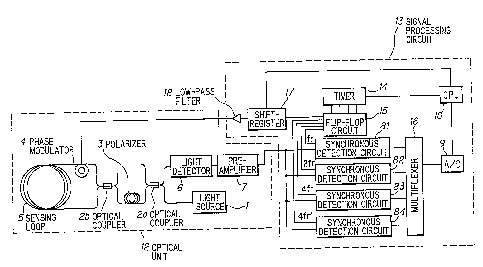
aforementioned conventional optical fiber gyro in Fig. 1 will be
explained.
The conventional optical fiber gyro comprises an optical
unit 12 and a signal processing unit 13. The optical unit 12
comprises a light source 1 for emitting a light stream, an optical
coupler 2a for coupling light streams to provide a coupled light
stream and decoupling a light stream to provide decoupled light
streams, a polarizer 3 for polarizing a light stream to provide a
polarized light stream, an optical coupler 2b for dividing the
polarized light stream into two light streams, a phase modulator 4
for modulating light streams in phase, an optical fiber sensing loop
5 for propagating the light streams in the clock-wise and counter
clock-wise directions, a light detector 6 for detecting a light
stream supplied from the optical coupler 2a, and a pre-amplifier 7
for amplifying an electric signal supplied from the light detector
6. The signal processing unit 13 comprises a synchronous detection
circuit 8 for separating fundamental, second and quadruple
harmonic wave components S1, S2, and S4 of a phase-modulation
frequency used in the phase modulator 4, an analog to digital (A/D)
converter 9 for converting the signals supplied from the synchronous
detection circuit 8 from analog to digital, a CPU (central processing
unit) 10 for calculating an angular velocity by receiving the digital
signals from the A/D converter 9, and an oscillator 11 for providing
the phase modulator 4 and
w _2144552
-12-
the synchronous detection circuit 8 with an oscillation signal in
accordance with the control of the CPU 10.
In operation, a light stream emitted from the light source
1 is branched by the optical coupler 2a, and one of the branched
light streams is polarized in the polarizer 3. A light polarized in
the polarizer 3 is branched by the optical coupler 2b, and one of the
branched light streams is modulated in phase to be propagated through
the sensing loop 5 in the counter clock-wise direction by the phase
modulator 4, while the other one of the branched light streams is
propagated through the sensing loop 5 in the clock-wise direction,
and then modulated in phase by the phase modulator 4. In the phase
modulator 4, a sine-wave signal applied from the oscillator 11
generates a constant phase bias for the light streams passed
therethrough. The light streams propagated through the sensing loop
5 are coupled by the optical coupler 2b, and the coupled light stream
is supplied via the polarizer 3 and the optical coupler 2a to the
light detector 6. When the sensing loop 5 is rotated to generate a
rotative angular velocity, a phase difference occurs between the
clock-wise and counter clock-wise direction propagated light streams,
so that a light stream received by the light detector 6 changes,
dependent on the phase difference. The light detector 6 generates
an electric signal which is then amplified in the pre-
CA 02144552 2001-O1-24
-13-
amplifier 7, and the amplified signal is detected in
the synchronous detection circuit 8 to separate a
fundamental wave component S1, a second harmonic
wave component S2, and a quadruple harmonic wave
component S4 of a phase modulation frequency .used in
the phase modulator 4. The fundamental wave component
S1, the second harmonic wave component S2, and the
quadruple harmonic wave component S4 are digitalixed
in the A/D converter 9 to be supplied to the CPU 10,
in which.an angular velocity is calculated in
accordance with the equations (2) to (6), as explained
before.
Fig. 2 shows an input signal having a frequency
of f~ supplied to the synchronous detection circuit
25 8, a synchronous signal f, for turning a switch on
and off in the synchronous detection circuit 8, a
detected output f, , and an output voltage f~
obtained by filtering the detected output f, by
using a low-pass filter (not shown), wherein the input
signal f~ and the synchronous signal f~ have a
phase difference of ~r /2 (90 degrees) therebetween.
Fig. 3 shows the input signal f~ , the
synchronous signal f, , the detected output f, ,
and the output voltage f~ , wherein the input signal
~5 f~ and the synchronous signal f, are coincident in
phase with each other.
The output voltage f. is zero in Fig. 2, while
the output voltage f, ie maximum in Fig. 3.
CA 02144552 2001-O1-24
_ 1
In the optical fiber gyro, the phase modulator
4 enhances the precision in detecting a rotative angular
velocity in accordance with the application of a phase
difference of approximately ~/2 on the propagating
light streams in the clock-wise and counter clock-wise
directions, and, if a phase of the synchronous signal
f2 deviates by even with a small amount, the linearity
in the sensing of a rotative angular velocity will
deteriorate. This is a reason. why the phase-adjustment
ZO of the synchronous signal f3 is necessary in the optical
fiber gyro.
Next, an optical fiber gyro in the first
preferred embodiment according to the invention will
be explained in Fig. 4, wherein like parts axe
indicated by like reference numerals as used in Fig. 1.
The optical fiber gyro comprises an optical unit 12
which is the same as explained in Fig.i,and a signal
processing circuit Z3 which .is improved in the
invention. The signal processing unit 13 comprises a
programmable timer 14 for generating a clock of an
arbitrary frequency bY dividing a reference clock, a
flip-flop circuit 15 operating in response to the clock from
the programmable timer 14 to generate a synchronous
signal, first to fourth synchronous detection circuits
B1 to 84 for synahronouely detecting a signal
supplied from a pre-amplifier 7 in accordance with
the switching-on and off by the synchronous signal
received from the flip-flop circuit 15, a shift register 17
CA 02144552 2001-O1-24
- 1 5 -
phase-shifting the synchronous signal supplied from
the flip-flop circuit 15 by receiving a shift clock ,and a
multiplexer 16 for selecting one of the outputs of the
first to fourth synchronous detection circuits 81 to
84. The signal .processing_cixcuit 13 further comprises
an A/D converter 9, a CPt1 10, and a filter 18.
sack of the synchronous detection circuits 81
to 84 carries out the synchronous detection of an
input signal in accordance with the synchronous
signal supplied from the flip-flop circuit 15.
zn this optioal fiber gyro, the first to fourth
synchronous detection circuits 81 to 84 provide a
fundamental wave synchronous detection circuit, an
even-number order harmonic wave synchronous detection
circuit, and an orthogonal component detection circuit,
and the timer 14, the flip-flop circuit 15, the shift register
17, and the CPU 10 provide means for adjusting a
phase of the synchronous detection circuit and a.phase
of the phase modulator 4.
A phase modulation signal fm which ie one of ON
and OFF signals generated iw- the flip-flop circuit 15 is
vazied in phase to be supplied to the phase modulator
4 by re-writing data supplied from the CPU 10 to the
timer 14 or the shift register 17. When the data
supplied to the timer 14 ie re-written, a phase
thereof is coarsely varied in the range of 360° (any
phase angle in one period), and, if the data supplied
tv the shift register 17 is re-written, the phase is
CA 02144552 2001-O1-24
-18-
finely varied.
First to fourth synohronaus signals which are
four signals of the ON and OFF signals generated in
the flip-flop circuit 15 are set. to have f requenoies o.f. a
f a n~ d a m a n t a 1 w a v a , second harmonic wave and
quadruple harmonic waves relative to a frequency of
the phase modulation signal fm. The synchronous
signals of the quadruple harmonic wave are of two
phases, one of which has a phase difference of 90°
( one quarter~period) relative to the other.
Hereinafter, the first one is defined as "In-phase
component synchronous signal", and the second one as "
Orthogonal component synchronous signal".
Fig. 5 shows the fundamental wave synchronous
signal fr, the second harmonic wave synchronous signal
2fr, the quadruple harmonic wave in-phase component
synchronous signal 4fr, and the quadruple harmonic wave
orthogonal component synchronous signal 4f'r which have
a phase-relation shown therein, wherein the signals fr, 2fr
and 4fr are symmetrical relative to a timing to, at which
the signals fr and 2fr are at the ON state, while the signal
4fr is at OFF state, and the signal 4fr' is changed OFF to ON
at the timing to-
~5 In the first preferred embodiment, the phase-
relation of~the synchronous signals fr, 2fr, 4fr and
4f'x as shown in Fig. 5 is fixed, and a phase of the
phase modulation signal fm is varied by re-writing the
CA 02144552 2001-O1-24
-ir-
data supplied to the timer 14 and the shift register
17.
In operation, the CPU 10 monitors a second
harmonic wave-detected output supplied from the
second synchronous detention circuit 82 via the
muitipiexer 16 to~the AID converter 9 to re-write the
data supplied to the timer 14, so that a phase of
the phase modulation signal fm is coarsely shifted to
make the second harmonic wave-detected output zero.
Nest, the CPU 10 monitors a quadruple harmonic wave
in-phase component-detected output in the same manner
to re-write the data supplied to the timer 14, so
that the phase of the phase modulation signal .fm is
coarsely shifted to make the quadruple harmonic wave
in-phase component-detected output zero. Then, the CPU
10 monitors a quadruple harmonic wave orthogonal
component-detected output in the same manner to re-
write the data supplied to the shift register 17, so
that the phase of the phase modulation signal fm is
finely shifted to make the quadruple harmonic wave
orthogonal component-detested output zero. This
sequential procedure is carried out under the control
of the CPU 10 having a predetermined program stored in
a ROM (not shown).
Thus, the guedrupie harmonic~wave orthogonal
component detested output ie controlled to be zero.
This means that Q 9 becomes zero in the equation (5).
Consequently, the values obtained in the equations
'95-03-10 18:12 HIRRTA ~ PARTNERS 03 3239 5463 P.21
_ . ..
2144552
-is-
(Z) to (4) beCOme maximum. The CPU 10 constantly
controls the timer 14 and theshift register l7to
carry out the above described phase adjustment, so
that .the , equations ( 2.?~ to ( 4 ? provide the 'maximum ,
values . . ~ ~ .. . .
More specifically, when a frequency of the
phase modulation signal fm is several tens of KHz, and a
frequency of the reference clock supplied to the
timer 14 is 10 MHa, the ooarse phase adjustment of
less than 4 degrees can be carried out fo;r a
quadruple harmonic wave, On the other hand, when:a
freguency of the shift clock supplied to the shift
register 17 is 48 MHz, the fine ghase adjustment of
less than 1 degrse can be carried out for a quadruple
harmonic wave. Consequently, the optical fiber gyro
is enhanced in precision and reliability in the first
pref erred embodiment.
As exglained above, it is preferable that the
phase adjustment and synchronous signals for the
ZO synohronous~detection are supplied from a common
oscillation source oscillating with a high frequency
to simply and precisely adjust phases in the phase
modulation and the synchronous detection. Practically,
a ref arence clock is generated, and a frequency of the
ZS reference clock is divided to provide a phase
modulation signal and synchronous signals. The
division of the reference clock is, advantageously
carried out in the programmable timer 14 which is
'95-03-10 18:12 HIRRTR & PRRTNERS 03 3239 5463 P.22
_ 2144552 ~ .
-1 s--
programmed by the CBU 10, so that an arbitrary
frequency of a clock is obtained at an arbitrary
phase. Zn this programmable timer 14, clocks of a
fundamental wave, an even-number order harmonic wane, ,
and an even-number order .harm.onic. ,wave .whiah~ is ~ ~ ~ .
shifted in phase by one quarter period are obtained. .
The shift. register 17 delays the clock of the
fundamental wave with a shift amount equal to a value
obtained by multiplying a shift clock by a constant
number in supplying~the clock of the fundamental wave
to the phase modulator 4. Thus, a phase relatipn
between the phase modulation signal and each
synchronous signal is determined dependently on a
mutual phase relation between fundamental Waves for
the phase modulation and the synchronous detection
generated in the programmable timer 14, and a phase
delayed in the shift register 17. This phase relation
is arbitrarily adjusted by setting a shift amount for
the shift register 17 and a program far the timer 14
ZO by the CPU 10. For this purpose, the CPU 10 monitors
an output of each synchronous detection circuit 81 to
84, so that the phase adjustment is carried out f,o
make the orthogonal component of the detected outputw
aero. '
As is apparent from the equations (2) to (4), a
phase adjustment precision depends on a scale of an
optical fiber gyro, wherein a scale error a is
approximately estimated by the highest order harmonic
CA 02144552 2001-O1-24
-20-
wave synchronously detected. In a case where the highest
order harmonic wave is a quadruple harmonic wave, the
equation (7) is defined.
~ ~. ti -cos c4 : e~ } x l.fl 0 .c~~ .. ........~7~
In order to fabricate an optical fiber gyro
having a scale error of less than 0.1$, a phase
adjustment precision of less than at least 0.6~° is
required.
fig. 6A shows an optical fiber gyro in the
second preferred embodiment according to the invention,
wherein like parts are indicated by like reference
numeral as used in Figs. i.and 4.
In the second preferred embodiment, a
programmable timer 1'4 and a flip-flopcircuit15 are
represented as a signal generator 20, and a D/A
converter 19 is further included, while a shift
register 17 (Fig. 4) is deleted. .
As shown in fig. 6B, the programmable timer 14
is typically composed of first to third timer circuits
14a, 14b and 14c for a synchronous signal, a,phase
modulation signal, and a control of a phase shift
amount by receiving control signals from the CPU 10,
and three counter circuits 14d for generating count
signals by receiving a clock signal from. the timer
circuit 14a. The flip-flop circuit 15 comprises first to third
JKflip-flop circuits 15d for generating three synchronous
CA 02144552 2001-O1-24
_2~_
signals fr, 2fr and 4fr for a fundamental wave, a
second harmonic wave, and a quadruple harmonic
wave, first and second inverters 15 a for
inverting the counter signals from the counte.f
circuits l4dr third tv f.ifth inverters lab for
inverting the synchronous signals fr, 2fr, and 4fr,
and fourth JK flip-flop circuit 15e for generating the phase
modulation signal fm, and a sixth inverter 7.5c for
inverting a clear signal from the CPU 10. The phase
modulation signal fm is oonverted from~digital to
analog by the D/A converter 17, and the converted
phase modulation signal fm is supplied via the low-
pass filter 18 to the phase modulator 4.
Fig. 7 shows a common structure of the
synchronous detection circuits 81 to 83, which each
comprises an analog switch 20 and a low-pass filter
(integration circuit) 2~., wherein the analog switch 20
is turned on and off by a corresponding one of the
synchronous signals generated in the flip-flop circuit 15, and
a detected signal is supplied via the low-pass filter
21 to the multiplexer 16.
Fig. 8 shows the multiplexex 16 comprising
fixst to third input terminals 22a, 22b and 22c for
receiving detected signals S~, S, and S~ from the
first to third synchronous detection circuits 81 to
83, an output terminal 23 for supplying a selected
one of the detected signals 8 ~, S~ and 8, to the A/D
converter 9, and input terminals 25a, 25b and 25c
CA 02144552 2001-O1-24
2
for receiving a switching-over signal fc from the CPv
to to switch aswitching circuit 24 to one of the input
terminals 22a, 22b and 220.
Fig, 9A shows operation of the second
synchronous detection circuit SZ to which an input
signal 5,~," and a synchronous signal 2fr of a
second harmonic wave is supplied, and from which
an .output signal S , s e~,, is obtained, wherein an
integrated value for the output signal 8~ie"c is
zero in level, because freguencies are not
synchronized between the input and synchronous signals
S,~,o and 2fr.
Fig. 9H shows operation of the second
synchronous detection circuit 82 to which an input
signal 9m ,p and a synchronous signal 2fr of the
second harmonic wave is supplied, and from which
an output signal S =yeas is obtained, wherein an
integrated value for the output signal S saa.v is
zero in level, because the phases differ by ~r/2
between the input and thesynchronoue signals 8,asa and
2fr.
In Figs. 9A and 9H, the detection o,f the
second harmonic wave component is explained. The
Same result is observed in the detection of the other
frequency components.
in the equations (2) to (4), the values of S',
S~ and S. are varied. when a phase of the phase
modulation signal fm is varied, even if the
CA 02144552 2001-O1-24
-23-
synchronous signals are fixed in phase.
Fig. 10 shows the synchronous signals fr, 2fr
and 4fr which are fixed in phase, and the phase
modulation signal fm which is varied in phase,
respectively, i~n the second preferred embodiment.
Under this assumption, Figs. 11A and 11B show the
relationship of the second and quadruple harmonic wave
outputs and a phase9 of the~phase modulation signal
fm on the condition that the sensing loop 5 is not
rotated, and clock-wise and counter clock-wise
direction light streams of a constant intensity and a
constant phase are supplied to the stationary sensing
loop 5, while the phase a of the phase modulation
signal fm is varied, so that the first term of the
equations (3) and (4) are considered as constant
values.
1n the phase modulation, the CFU 10 monitors a
detected output of the second synchronous detection
circuit 82 for detecting the second harmonic wave
signal S ,., and, at the same time, controls the
signal generator 20 to ahift-.a phase of the phase
modulation signal fm which is coarsely adjusted, so
that the second harmonic wave signal SZ will be
zero (offeat level) as shown in Fig.llA. Subsequently,
the signal generator 20 ~.s controlled to shift tha
phase of the phase modulation signal fm in a positive
output direction of the second harmonic wave signal
8s by one-eighth wavelength (equal to 45 degrees) of
CA 02144552 2001-O1-24
_24_
the second harmonic wave signal SZ . Then, the
switching circuit 24 of the multiplexer 16 is switched
to the input terminal 22c, .so that a detected output
of the quadruple harmonic wave signal S. is monitored
by the CPU 10. Simultaneously, the signal generator
20 is controlled to finely shift the phase of th.e
phase modulation signal fm, so that the detected
output of the quadruple harmonic wave signal Ss will
be zero (offset level). Then, the signal generator ZO
is controlled to shift the phase of the phase
modulation signal fm in a positive output direction
of the guadruple harmonic wave signal S~ by one-
eighth wavelength (equal to 45 degrees) of the
second harmonic wave signal SZ as shown in ~'ig.
11B.
In this manner, the phase of the phase
modulation signal fm is adjusted with a high precision.
In the coarse and fine adjustments, the above
described zero level (the offset level) is a level
equal to output levels of the first to third
synchronous detection circuits 81 to 83 in a case where
the phase modulator 4 is not driven, or the
light source 1 is turned off, wherein a subsequent one
of the output levels thereof is successively detected
by switching-over the multiplexer 16, so that data
thus sampled are supplied via the A/D converter 9 to
the CPU 10, in which the data are processed in
accordance with addition and mean value
CA 02144552 2001-O1-24
- 2 6 -
calculationscarried out by a program stored in the CPU
10.
In the signal generator 20 comprising the timer
14 and the flip-flop circuit 15, the timer circuit 14a of the
timer 14 generates a'clock signal for driving the
three counters 14d of the timer 14 to generate count
signals, and the JK flip-flop circuit 15e of the flip-flop circuit 15
shifts the phase of the phase modulation signal fm by
receiving the clock signal from the timer circuit 14b.
1~ More specifically, the JK flip-flop circuit 15e for the
phase adjustment operates with set and reset states
by receiving the clock signal from the timer circuit
14b, while the timer circuit 14c for the control of
phase shift amount continues counting up to a value
15 set by the CeU 10, and, when a counted value of the
timer circuit 14c becomes equal to the value set by
the CPU 10, the JK flip-flop circuit 15e for the generation of
the phase modulation signal fm is cleared to
precisely control the phase shift amount.
20 In the second preferred embodiment, a precision
of less than 1 degree is obtained in the phase
adjustment, when a frequency of the phase modulation
signal,fm is several tens of KHz and a frequency of
the clock signal supplied to the timex 14 is 10 MFi~.
25 Consequently, the precision and the reliability of
the optical fiber gyro are markedly enhanced in ~,he
second preferred embodiment.
In the second preferred embodiment, the phase
CA 02144552 2001-O1-24
-26-
adjustment of the phase modulation signal fm is
automatically Carried out to shorten a time for the
phase adjustment, and a one-phase synchronous
detection circuit can be used to make a circuit size
small and decrease fabrication cost and product
cost.
~n the second preferred embodiment, the
synchronous signals fr, 2fr and 4fr may be shifted in
phase in place of shifting a phase of the phase
modulation signal fm. In such a case, the three JK
flip-flop circuits 15d for the synchronous signals fr, 2fr and
Afr are set and reset by receiving the clock signal
and the count signals, while timer circuit 1Ac for
the control of a phase shift amount continues counting
up to a value set by the CPU 10, and the JK flip-flop circuit
15e is cleared to precisely control the phase shift
amount, when a counted value is equal to the set
value.
In the first and second preferred embodiments,
the coarse and fine adjustments are parried out at the
zero-crossing points of the second and quadruple
harmonic wave outputs S~ and Ss as shown in Figs.
11A and iis. As a result, the precision of the phase
adjustment is remarkably increased, because the
change rate of the outputs s, and S~ is maximum at
the zero-crossing points as compared to other points.
Further, the phase adjustment is correctly carried
out, when the offset levels as shown in Figs. 11A and
'95-03-10 18:16 HIRATR & PARTNERS 03 3239 5463 P.30
_ 214452. . : ..
- 2 7 -
11B are set to be approximately the noise level of an
electric signal processing system including a power
supply, the pre-amplifier 7, the synchronous detection
c.i,rcuits , 81 to 83 , etc. , so that any inf luence. ~ of
noise~~is avoided in the phase adjustment. .
Although the invention has been described with
respect to specific embodiments for complete and clear
disclosure, the appended claims are not to be~ thus
limited but are to be construed as embodying all
modifications and alternative constructions that may
occur to one skilled in the art which fairly fall
within the basic teaching h~rein set forth.
1S
25