Sélection de la langue

Search

Sommaire du brevet 2145396 

Énoncé de désistement de responsabilité concernant l'information provenant de tiers

Une partie des informations de ce site Web a été fournie par des sources externes. Le gouvernement du Canada n'assume aucune responsabilité concernant la précision, l'actualité ou la fiabilité des informations fournies par les sources externes. Les utilisateurs qui désirent employer cette information devraient consulter directement la source des informations. Le contenu fourni par les sources externes n'est pas assujetti aux exigences sur les langues officielles, la protection des renseignements personnels et l'accessibilité.

Disponibilité de l'Abrégé et des Revendications

L'apparition de différences dans le texte et l'image des Revendications et de l'Abrégé dépend du moment auquel le document est publié. Les textes des Revendications et de l'Abrégé sont affichés :

  • lorsque la demande peut être examinée par le public;
  • lorsque le brevet est émis (délivrance).
(12) Demande de brevet: (11) CA 2145396
(54) Titre français: COMMUTATEUR DE TELECOMMUNICATION PROGRAMMABLE POUR ORDINATEUR PERSONNEL
(54) Titre anglais: PROGRAMMABLE TELECOMMUNICATION SWITCH FOR PERSONAL COMPUTER
Statut: Réputée abandonnée et au-delà du délai pour le rétablissement - en attente de la réponse à l’avis de communication rejetée
Données bibliographiques
(51) Classification internationale des brevets (CIB):
  • H04Q 03/545 (2006.01)
  • H04Q 03/62 (2006.01)
  • H04Q 11/04 (2006.01)
(72) Inventeurs :
  • MADONNA, ROBERT P. (Etats-Unis d'Amérique)
  • BUTTEL, ROBERT J. (Etats-Unis d'Amérique)
  • HEBERT, MARK P. (Etats-Unis d'Amérique)
(73) Titulaires :
  • EXCEL SWITCHING CORPORATION
(71) Demandeurs :
  • EXCEL SWITCHING CORPORATION (Etats-Unis d'Amérique)
(74) Agent: KIRBY EADES GALE BAKER
(74) Co-agent:
(45) Délivré:
(86) Date de dépôt PCT: 1993-09-15
(87) Mise à la disponibilité du public: 1994-04-14
Requête d'examen: 2000-08-15
Licence disponible: S.O.
Cédé au domaine public: S.O.
(25) Langue des documents déposés: Anglais

Traité de coopération en matière de brevets (PCT): Oui
(86) Numéro de la demande PCT: PCT/US1993/008724
(87) Numéro de publication internationale PCT: US1993008724
(85) Entrée nationale: 1995-03-23

(30) Données de priorité de la demande:
Numéro de la demande Pays / territoire Date
07/953,690 (Etats-Unis d'Amérique) 1992-09-29

Abrégés

Abrégé anglais


A user-programmable telephone switch which resides within
a commercially available personal computer. The switch is
controllable by either the personal computer's microprocessor
or a separate, external host connected to an interface provided
within the switch. The switch includes a CPU/matrix card that
contains a time slot interchange and a CPU running under a real
time operating system. The CPU/matrix card controls the
overall operation of the switch in accordance with messages
received from the operative host. In general, those tasks or
functions which must be performed in real time are the
responsibility of the switch, as opposed to the internal or
external host. Within the switch, certain tasks or functions
may be delegated by the CPU/matrix card to intelligent line
cards which contain their own microprocessors having
substantial call processing capability.

Revendications

Note : Les revendications sont présentées dans la langue officielle dans laquelle elles ont été soumises.


-12-
CLAIMS
1. A programmable communications switch (10) comprising
controllable-switching means (12) for dynamically connecting or
disconnecting communication paths between various ones of a
plurality of ports in response to predetermined messages,
including means for processing said messages (34), a time slot
interchange (44) and a real time operating system characterized
in that said switching means resides in a first host computer
(2), said first host computer for providing electrical power to
said switching means, having a first application-oriented
operating system and being programmable to generate said
messages, means (32) for interfacing said switching means with
a second host computer (30) having a second application-
oriented operating system and being programmable to generate
said messages, and means (35), coupled to the message
processing means, for selecting one of said first and second
host computers to control said controllable-switching means.
2. The switch as in claim 1 wherein said first host computer
comprises a personal computer motherboard which includes an
input/out bus (8) and a power bus (9), and said switching means
is connected to both of said busses.
3. The switch as in claim 2 further comprising one or more
line cards (14, 18), connected in communicating relationship
with said switching means, for terminating either digital or
analog lines or trunks.
4. The switch as in claim 3 wherein each of said one or more
line cards for terminating digital lines or trunks includes
means for processing (46) messages generated by said switching
means.

-13-
5. The switch as in claim 4 wherein said message processing
means of said switching means is operable to distinguish
between said one or more line cards and may assign
responsibility to said digital line card message processing
means for performing one or more predetermined call processing
tasks, while retaining responsibility for performing such tasks
with respect to said analog line cards.
6. The switch as in claim 1 further comprising means (42),
responsive to the message processing means, for selecting one
of a plurality of synchronization signals available thereto.
7. The switch as in claim 1 wherein said second host
computer is connected with said interfacing means and
exclusively controlling said switching means without said first
host computer.
8. The switch as in claim 1 wherein said messages are
generated by said host in accordance with a predetermined
format which is independent of the types of line cards
connected to said switching means.
9. The switch as in claim 3 wherein said analog line cards
are connected in communicating relationship with said switching
means by a bus (22) for carrying time division multiplex data,
a timing/control bus (26) and a line card status/control bus
(24).
10. The switch as in claim 1 wherein each of said analog line
cards includes means for responding to an interrogation by said
message processing means of said switching means by identifying
one or more types of signalling protocol modules located on
said analog line card.
11. The switch as in claim 1 wherein each of said analog line
cards includes means (64) for responding to an interrogation by

-14-
said message processing means of said switching means by
indicating the number of signalling protocol modules located on
said analog line card.
12. The switch as in claim 3 wherein said digital line cards
are connected in communicating relationship with said switching
means by a bus (20) for carrying messages bidirectionally, a
bus for carrying time division multiplex data, and a
timing/control bus.
13. The switch as in claim 4 wherein the message processing
means (46) of each of said digital line cards transmits one or
more messages to the message processing means of the switching
means which indicates the status of the digital line card.
14. The switch as in claim 1 wherein the message processing
means (46) of each of said digital line cards transmits one or
more messages to the message processing means of the switching
means which indicates the types of ports provided by the
digital line card.
15. The switch as in claim 1 wherein the message processing
means (46) of each of said digital line cards transmits one or
more messages to the message processing means of the switching
means which indicates how many ports are provided on the
digital line card.
16. The switch as in claim 1 wherein the message processing
means (46) of each of said digital line cards transmits one or
more messages to the message processing means of the switching
means which indicates whether a download of instructions is
needed by the digital line card.
17. The switch as in claim 16 wherein the message processing
means (34) of the switching means, in response to receiving a

-15-
message from a digital line card indicating that a download of
instructions is needed, downloads instructions to said digital
line card.
18. The switch as in claim 17 wherein the message processing
means (34) of the switching means downloads instructions to
said digital line card which include instructions for
signalling supervision.
19. The switch as in claim 17 wherein the message processing
means (34) of the switching means downloads instructions to
said digital line card which include instructions for call
inpulsing and outpulsing.
20. The switch as in claim 17 wherein the message processing
means (34) of the switching means downloads instructions to
said digital line card which include instructions for detection
of incoming calls.
21. The switch as in claim 17 wherein the message processing
means (34) of the switching means downloads instructions to
said digital line card which include instructions for
generation of outgoing calls.
22. A programmable communications switch (10) comprising
controllable-switching means (12) for dynamically connecting or
disconnecting communication paths between various ones of a
plurality of ports in response to predetermined messages,
including means for processing said messages (34), a time slot
interchange (44) and a real time operating system characterized
in that said switching means resides in a first host computer
(2), said first host computer for providing electrical power to
said switching means, having a first application-oriented
operating system and being programmable to generate said
messages, means (20, 22, 24, 26) for connecting one or more

-16-
line cards (14, 18) in communicating relationship with said
switching means, each of said one or more line cards for
terminating either analog lines or trunks or digital lines or
trunks, each of said digital line cards including processing
means (46) for performing one or more predetermined call
processing tasks, said message processing means being operable
to distinguish between said analog and digital line cards,
whereby said message processing means may assign responsibility
to said digital line card processing means for performing said
one or more predetermined call processing tasks, while
retaining responsibility for performing such tasks with respect
to said analog line cards.
23. The switch as in claim 22 wherein said messages are
generated by said host in accordance with a predetermined
format which is independent of the types of line cards
connected to said switching means.
24. The switch as in claim 22 further comprising means (32)
for interfacing said switching means with a second host
computer (30) having a second application-oriented operating
system and being programmable to generate said messages and
means (35), coupled to the message processing means, for
selecting one of said first and second host computers to
control said switching means.
25. The switch as in claim 22 wherein said first host
computer comprises a personal computer motherboard which
includes an input/output bus (8) and a power bus (9), and said
switching means is connected to both of said busses.
26. The switch as in claim 22 further comprising means (42),
responsive to the message processing means (34), for selecting
one of a plurality of synchronization signals available
thereto.

-17-
27. The switch as in claim 24 wherein said second host
computer is connected with said interfacing means and
exclusively controlling said switching means without said first
host computer.
28. The switch as in claim 22 wherein said analog line cards
are connected in communicating relationship with said switching
means by a bus for carrying time division multiplex data (22),
a timing/control bus (26) and a line card status/control bus
(24).
29. The switch as in claim 22 wherein each of said analog line
cards includes means (64) for responding to an interrogation by
said message processing means of said switching means by
identifying one or more types of signalling protocol modules
located on said analog line card.
30. The switch as in claim 22 wherein each of said analog line
cards includes means (64) for responding to an interrogation by
said message processing means of said switching means by
indicating the number of signalling protocol modules located on
said analog line card.
31. The switch as in claim 22 wherein said digital line
cards are connected in communicating relationship with said
switching means by a bus for carrying messages bidirectionally
(20), a bus for carrying time division multiplex data (22), and
a timing/control bus (26).
32. The switch as in claim 22 wherein the processing means
(46) of each of said digital line cards transmits one or more
messages to the message processing means (34) of the switching
means which indicates the status of the digital line card.
33. The switch as in claim 22 wherein the processing means
(46) of each of said digital line cards transmits one or more

-18-
messages to the message processing means (34) of the switching
means which indicates the types of ports provided by the
digital line card.
34. The switch as in claim 22 wherein the processing means
(46) of each of said digital line cards transmits one or more
messages to the message processing means (34) of the switching
means which indicates how many ports are provided on the
digital line card.
35. The switch as in claim 22 wherein the processing means
(46) of each of said digital line cards transmits one or more
messages to the message processing means (34) of the switching
means which indicates whether a download of instructions is
needed by the digital line card.
36. The switch as in claim 37 wherein the message processing
means (34) of the switching means, in response to receiving a
message from a digital line card indicating that a download of
instructions is needed, downloads instructions to said digital
line card.
37. The switch as in claim 38 wherein the message processing
means (34) of the switching means downloads instructions to
said digital line card which include instructions for
signalling supervision.
38. The switch as in claim 38 wherein the message processing
means (34) of the switching means downloads instructions to
said digital line card which include instructions for call
inpulsing and outpulsing.
39. The switch as in claim 38 wherein the message processing
means (34) of the switching means downloads instructions to
said digital line card which include instructions for detection
of incoming calls.

-19-
40. The switch as in claim 38 wherein the message processing
means (34) of the switching means downloads instructions to
said digital line card which include instructions for
generation of outgoing calls.
41. A programmable communications switch (10) comprising
controllable-switching means (12) for dynamically connecting or
disconnecting communication paths between various ones of a
plurality of ports in response to predetermined messages,
including means for processing said messages (34), a time slot
interchange (44) and a real time operating system characterized
in that said switching means resides within a first host
computer (2) comprising a personal computer motherboard that
includes an input/output bus (8) and a power bus (9), said
switching means being connected to both of said busses, said
first host computer having a first application-oriented
operating system and being programmable to generate said
messages, means (32) for interfacing said switching means with
a second host computer having a second application-oriented
operating system and being programmable to generate said
messages, means (35) coupled to the message processing means
for selecting one of said first and second host computers to
control said controllable-switching means, one or more line
cards (14, 18) connected in communicating relationship with
said switching means, each of said one or more line cards for
terminating either analog lines or trunks or digital lines or
trunks, each of said digital line cards including means (46)
for processing messages generated by said switching means and
performing one or more predetermined call processing tasks,
said message processing means (34) of said switching means
being operable to distinguish between said one or more line
cards and to assign responsibility to said digital line cards
for performing one or more predetermined call processing tasks,
while retaining responsibility for performing said tasks with
respect to said analog line cards.

-20-
42. The switch as in claim 43 further comprising means (42),
responsive to the message processing means, for selecting one
of a plurality of synchronization signals available thereto.
43. The switch as in claim 43 wherein said messages are
generated by said host computers in accordance with a
predetermined format which is independent of the types of line
cards connected to said switching means.
44. The switch as in claim 43 wherein said analog line cards
are connected in communicating relationship with said switching
means by a bus (22) for carrying time division multiplex data,
a timing/control bus (26) and a line card status/control bus
(24).
45. The switch as in claim 43 wherein each of said analog line
cards includes means (64) for responding to an interrogation by
said message processing means of said switching means by
identifying one or more types of signalling protocol modules
located on said analog line card.
46. The switch as in claim 43 wherein each of said analog line
cards includes means (64) for responding to an interrogation by
said message processing means of said switching means by
indicating the number of signalling protocol modules located on
said analog line card.
47. The switch as in claim 43 wherein said digital line
cards are connected in communicating relationship with said
switching means by a bus (20) for carrying messages
bidirectionally, a bus (22) for carrying time division
multiplex data, and a timing/control bus (26).
48. The switch as in claim 43 wherein the message processing
means (46) of each of said digital line cards transmits one or

-21-
more messages to the message processing means (34) of the
switching means which indicates the status of the digital line
card.
49. The switch as in claim 43 wherein the message processing
means (46) of each of said digital line cards transmits one or
more messages to the message processing means (34) of the
switching means which indicates the types of ports provided by
the digital line card.
50. The switch as in claim 43 wherein the message processing
means (46) of each of said digital line cards transmits one or
more messages to the message processing means (34) of the
switching means which indicates how many ports are provided on
the digital line card.
51. The switch as in claim 43 wherein the message processing
means (46) of each of said digital line cards transmits one or
more messages to the message processing means (34) of the
switching means which indicates whether a download of
instructions is needed by the digital line card.
52. The switch as in claim 53 wherein the message processing
means (34) of the switching means, in response to receiving a
message from a digital line card indicating that a download of
instructions is needed, downloads instructions to said digital
line card.
53. The switch as in claim 54 wherein the message processing
means (34) of the switching means downloads instructions to
said digital line card which include instructions for
signalling supervision.
54. The switch as in claim 54 wherein the message processing
means (34) of the switching means downloads instructions to

-22-
said digital line card which include instructions for call
inpulsing and outpulsing.
55. The switch as in claim 54 wherein the message processing
means (34) of the switching means downloads instructions to
said digital line card which include instructions for detection
of incoming calls.
56. The switch as in claim 54 wherein the message processing
means (34) of the switching means downloads instructions to
said digital line card which include instructions for
generation of outgoing calls.

Description

Note : Les descriptions sont présentées dans la langue officielle dans laquelle elles ont été soumises.


W094/0~30 2 1 4 ~ ~ 9 6 PCT/US93/087~
PROGRAMMABLE TELECOMMWICATION
SWITCH FOR PERSONAL COMPUTER
BACKGROUND OF THE lNV~NlION
1. Field of the Invention
The present invention relates generally to the field of
telecommunications and, more specifically, to a programmable
telecommunication switch which may reside within a personal
computer.
2. Discussion of the Prior Art
User-programmable telecommunication switches are used in a wide
variety of applications such as voice messaging, telemarketing
services and the like. A programmable switch is usually
controlled by a host device, which is typically a computer that
runs an application program. A customer may either purchase a
commercially available application program that is compatible
with the host and switch hardware or may elect to write a
custom program.
As the application program runs, the host issues instructions
to the switch by way of a communication channel. The switch
responds to these instructions by taking appropriate action,
which may include issuing a response to the host to confirm
receipt or execution of the instructions.
Conventional programmable switches exhibit several
disadvantages which unduly limit their utility in many
applications. For example, a conventional switch that requires
its host device to become involved with call processing tasks
that must be performed in ~real time" creates a significant
processing burden on the host. The term ~real time" is used
herein to refer generally to call processing (e.g., sending or
receiving digits) or other tasks which must be executed within
a time period on the order of tens of milliseconds. If the
host is running under an operating system, such as DOS~ or
UNIX~, which is user or application-oriented and not designed
for real time operation, the real time demands made by the
switch will tend to monopolize the host's processing resources.

- . . .--. . .--. .--.:
- 2 1 ~ 6
This may, in turn, force the customer to undesirably limit the
amount of traffic through the switch so that the host can
maintain control.
This problem is not satisfactorily solved by simply installing
a real time operating system on the host. This is because the
multitude of real time call processing tasks generated by a
switch having a few hundred ports would still occupy so much of
the host's resources that the application program could not run
properly. Moreover, most commercially available computers
which could be used as hosts do not operate on any widely used
real time operating system. Prospective customers express a
strong preference, if not an absolute demand, for a host
operating system that is widely used and represents no
significant barrier to developing custom applications software.
Another disadvantage of conventional programmable switches is
that they can only be connected to one host at a time. This
means that should the host malfunction or fail, the switch will
not be controllable and service will be impaired or completely
lost.
EP 0 350 4-02 discloses the integration of an ISDN digital
subscriber terminal within a personal computer (PC). However,
the subscriber terminal does not function as a programmable
telecommunications switch, is not controllable by a second,
alternate PC or other host device, and does not provide
delegation of call processing responsibility according to the
available types of line interfaces.
DE 35 34 918 discloses a PC which is connected to and
controls a telephone structural unit that interfaces with
exchange and subscriber lines. The telephone structural unit
does not provide for control by a second, alternate host
device, and does not provide delegation of call processing
responsibility according to the available types of line
interfaces.
EP 0 358 597 discloses an ISDN peripheral which is
controlled by a PC. The peripheral does not provide for
AMENDED SHEE~

2145~6
-- -- . .
-- -- ---- . --
-- . .. .
-------- ------------
: ._2A_ . . - -
control by a second, alternate host device, and does not
provide delegation of call processing responsibility according
to the available types of line interfaces.
ICC '90 (Paper 211.3, vol. 1, April 15, 1990, pages 128-
133) discloses a small telephone system or PBX in which the
users' station sets include interfaces for PCs. The system
does not function as a programmable telecommunications switch,
is not controllable by a second, alternate PC or other host
device, and does not provide delegation of call processing
responsibility according to the available types of line
interfaces.
SUMMARY OF THE INVENTION
In brief summary, the present invention provides a user-
programmable telephone switch which resides within a
commercially available personal computer. The personal
computer, which typically runs on a widely used, application-
oriented operating system, provides a platform for customers
that is both easy to program and readily integratable into
existing communication networks.
The switch is controllable by the personal computer~s central
processing unit (PC CPU), a motherboard or plug-in PC CPU, any
of which may act as an ~'internal~' host. Alternatively, the
switch is controllable by a separate, external host connected
to an interface provided within the switch.
When an internal host is used, all real time call processing is
handled by the switch independent of the internal host. None
of the internal host's resources (microprocessor, memory, disk,
A~ENDE3 SHEET

W094/0~30 2 1 4 5 3 9 6 PCT/US93/08724
etc.) is needed to execute time-critical, real time tasks.
Thus, all of the internal host's resources are available for
use by the application program.
When an external host is used, none of the internal host's
resources is needed to control the switch or perform real time
call processing tasks. The external host's resources are
available for use by the application program and the internal
host may be used for a completely different application or,
alternatively, held in reserve as a back-up should the external
host fail. Also, when an external host is used, all that is
required to make the switch operable is a passive backplane for
supplying electrical power.
Physically, the switch comprises a plurality of circuit boards
or cards which are dimensioned to fit within the chassis of the
personal computer. A CPU/matrix card contains a time slot
interchange and a central call processor (microprocessor)
running under a real time, multi-tasking operating system. The
CPU/matrix card, which includes circuitry for selecting either
the internal host or external host to control the switch,
conducts all communication with the host. The CPU/matrix card
performs or delegates to other intelligent cards within the
switch the performance of all real time call processing tasks,
thus freeing the host from involvement in any real time tasks.
Four busses provide communication paths between the CPU/matrix
card and other cards within the switch: a timing/control bus;
a line card status/control bus; a time division multiplex (TDM)
bus for carrying pulse coded modulation (PCM) voice traffic and
analog line signalling; and an HDLC or interprocessor bus. A
fifth bus, the battery/ring voltage bus, is connected only to
line cards which terminate analog lines or trunks. These five
busses are used exclusively by the programmable switch and do
not interfere with communications within the internal host,
such as those between the PC CPU and disk controllers, video
graphics cards, serial or parallel ports or LAN controllers.
Digital (T1) line cards are provided for terminating digital
lines or trunks. Each digital line card includes its own

W094/08430 2 1 4 ~ 3 9 ~ PCT/US93/0872~
-4-
microprocessor which, under instructions from the CPU/matrix
card, may be used to perform certain-real time call processing
tasks on board the line card. Digitàl line cards communicate
with the CPU/matrix card over the;~DLC bus.
Analog line cards are provided for terminating analog lines or
trunks. Each analog line card may be configured with different
modules to terminate lines or trunks having different types of
signalling protocols on the same card.
Other optional cards, such as a digital signal processor (DSP)
card, may be incorporated into the switch to provide desired
services or features.
In accordance with one aspect of the present invention, tasks
are architecturally divided according to whether they require
real time processing. Those tasks which must be performed in
real time are the responsibility of the switch, as opposed to
the internal or external host. Further, within the switch,
certain tasks or functions may be delegated by the CPU/matrix
card to, for example, digital line cards which contain their
own microprocessors having substantial call processing
capability. This process of delegation is carried out
automatically and transparently to the host. Consequently, the
host is relieved of dealing with real time tasks, which tend to
reduce efficiency and processing speed, and the CPU/matrix card
is relieved of dealing with tasks pertaining to digital ports
that are within the capability of a digital line card's
processor.
Another advantage of the present invention is the high speed of
host-to-switch messaging between the personal computer
motherboard and the switch which resides thereon. This high
messaging speed is achieved by using the standard personal
computer bus as the communication channel between the internal
host and the CPU/matrix card.

W094/0~30 2 1 4 5 3 9 6 PCT/US93/08724
_ -5-
BRIEF DESCRIPTION OF THE DRAWINGS
This invention is pointed out with particularity in the
appended claims. The above and further advantages of this
invention may be better understood by referring to the
following description taken in conjunction with the
accompanying drawings, in which:
Figure 1 is a block diagram of a programmable
telecommunications switch which resides in a personal computer
and which is constructed in accordance with a preferred
embodiment of the present invention;
Figure 2 is a detailed diagram of the CPU/matrix card of Figure
l;
Figure 3 is a detailed diagram of the digital line card of
Figure 1; and
Figure 4 is a detailed diagram of the analog line card of
Figure 1.
DETAILED DESCRIPTION OF AN ILLUSTRATIVE EMBODIMENT
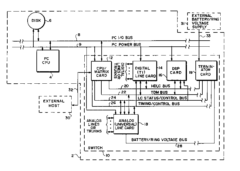
Figure 1 shows a commercially available personal computer
(PC) 2 which includes a PC central processing unit (CPU) 4 and
a hard disk drive 6 interconnected by a PC input/output (I/O)
bus 8 and a PC power bus 9. The PC 2 is preferably a PC-AT~,
sold by International Business Machines, or a compatible
thereof. Other personal computers having more memory or more
powerful CPUs than the PC-AT~ may also be used. The PC 2
preferably operates under an application-oriented operating
system, such as DOS~ or UNIX~.
The PC 2 consists of a chassis or housing in which a
motherboard is mounted, along with the disk drive 6 and other
optional assemblies such as floppy disk drives, modems and the
like. The PC CPU 4 is mounted on the motherboard, which
includes a series of "slots" into which other boards (cards)
may be inserted and thereby connected to the PC I/O and power
busses 8 and 9.
A programmable telecommunication switch 10 resides within
the PC 2. A CPU/matrix card 12 is inserted into one of the

WOg4/0~ ~ 2 1 4 ~ 3 9 6 PCT/US93/0872~
-6-
slots on the motherboard and thus connected to the busses 8 and
9. The CPU/matrix card 12 is interconnected with a digital
(Tl) line card 14, a digital signal processing (DSP) card 16
and an analog (universal) line card 18 and a terminator card 19
by four busses: an HDLC or interprocessor bus 20; a TDM bus
22; a line card (LC) status/control bus 24; and a
timing/control bus 26. A battery/ring voltage bus 28 supplies
battery voltage (48VDC) and ringing voltage (109VAC) to the
analog line card 18. The terminator card 19 serves to
physically terminate busses 20, 22, 24, 26 and 28.
The line cards 14 and 18 and the DSP card 16 are all
connected to and receive their basic operating power from the
PC power bus 9. Although only one digital line card 14 and one
analog line card 18 are depicted, it should be understood that
additional line cards of either type may be added subject to
two physical limitations: (1) the maximum switching capacity
of the CPU/matrix card 12, and (2) the physical space within
the chassis of the PC 2.
An external host 30, which may comprise a separate
personal computer, workstation or other computer, may
optionally be connected via a communication channel 32 to the
CPU/matrix card 12. The CPU/matrix card 12 preferably includes
a conventional RS-232 compatible interface for connecting the
channel 32. The external host 30 preferably operates under an
application-oriented operating system.
If desired, the switch 10 can reside on a passive
backplane (no PC CPU 4 or disk 6 present) from which its
receives electrical power and be controlled by the external
host 30.
An external battery/ring voltage supply 31 is connected
via a path 33 to the terminator card 19. Supply 31 may
comprise, for example, a commercially available power supply.
Figure 2 shows the CPU/matrix card 12 in greater detail.
A central call processor 34 is connected to both the HDLC bus
20 and the LC status/control bus 24. The central call

214539fi
W094/08430 PCT/US93/08724
--7--
processor 34 is also connected with host select circuitry 35,
random access and read only memories 36, watchdog timing
circuitry 38, input/output (I/O) control circuitry 40, timing
and control/select circuitry 42 and a time slot interchange
tTSI) 44. Timing and control/select circuitry 42 is connected
to the TSI 44, the timing/control bus 26 (for loop timing) and
to three sources of timing signals, which are denoted REF 1,
REF 2 (which may be supplied by external sources for reference
timing) and OSCILLATOR (which may be supplied by a free running
oscillator located on the CPU/matrix card 12), respectively.
The central call processor 34, which is preferably a
Motorola 68302 microprocessor, has control over all of the
other circuitry on the CPU/matrix card 12. The central call
processor 34 preferably runs under a real time operating system
such as pSOS~, sold by Integrated Systems, and preferably uses
Q.931-like messages, a CCITT standard protocol, for
communicating over the HDLC bus 20. Using the HDLC bus 20, the
central call processor 34 may transmit a message simultaneously
to all cards connected to that bus. The processor 34 may use
the LC status/control bus 24 to select a particular card to
transmit a message over the HDLC bus 20.
The host select circuitry 35, which is preferably a
switch, operates to inform the processor 34 whether to
communicate with the internal host or the external host upon
power-up.
I/O control circuitry 40, which manages all communication
between the central call processor 34 and the internal host,
preferably appears as a COMM port or other standard PC I/O port
on the PC I/O bus 8.
Timing and control/select circuitry 42, as described
further below, operates in response to instructions from the
central call processor 34 to select one of five available
signals for synchronizing the CPU/matrix card 12. Two such
signals are provided by the timing/control bus 26, the other
three being REF 1, REF 2 and OSCILLATOR.

W O 94/08430 2 1 ~ 5 3 9 ~ -8- PC~r/US93/08724
TSI 44, which is preferably a 512 port non-blocking
matrix, receives incoming PCM voice data via the TDM bus 22
(time slots) and operates, as directed ~y the central call
processor 34, to reorder the time slots and direct them over
the bus 22 to the appropriate dest~ations.
Figure 3 shows the digital line card 14 of Figure 1 in
greater detail. The line card 14 includes a line card
processor 46 which is connected with the HDLC bus 20, random
access and read only memories 48, digital select circuitry 50,
HDLC select circuitry 51, elastic stores 52a-52n, dual framers
54a-54n and dual Tl interfaces (IF) 56a-56n. Timing and
control circuitry 54 is connected to the timing and control bus
26, identification (ID) circuitry 49, the digital select
circuitry 50, the elastic stores 52a-52n, the dual framers 54a-
54n and the dual Tl interfaces 56a-56n.
Line card processor 46, which is preferably a Motorola
68302 microprocessor, has control over the other circuitry on
line card 14. Processor 46 communicates with the central call
processor 34 on the CPU/matrix card 12 by exchanging messages
over the HDLC bus 20. HDLC select circuitry 51, under the
control of processor 46, is responsible for controlling the
transmission of messages by the line card 14 over the HDLC bus
20.
Digital select circuitry 50 is responsible for moving PCM
traffic between the TDM bus 22 and the elastic stores 52a-52n.
On the digital line card 14, the PCM traffic represents only
voice, tone or data and does not include any line signalling
information.
Each dual Tl interface 56a-56n is capable of terminating
two Tl spans, thus providing a maximum of 96 DS0 ports, out of
the total of 512 ports available on the CPU/matrix card 12, per
digital line card 14.
Turning now to Figure 4, analog line card 18 includes
timing and control circuitry 58, which is connected to the LC
statusicontrol bus 24, the timing/control bus 26, digital

2145396
W094/0~30 PCT/US93/08724
_g_
select circuitry 60 and identification (ID) circuitry 64, which
is similar to ID circuitry 49 of Figure 3. Digital select
circuitry 60 is connected to analog interfaces 62a-62n. LC
status/control bus-24 and battery/ring voltage bus 28 are
connected to each analog interface 62a-62n.
Timing and control circuitry 58 communicates with the
central call processor 34 on CPU/matrix card 12 via the LC
status/control bus 24.
Digital select circuitry 60 is responsible for moving PCM
traffic between the TDM bus 22 and the analog interfaces 62a-
62n. In contrast with the digital line card 14, the PCM
traffic between the analog line card 18 and the TDM bus may
also contain line signalling information such as on-hook/off-
hook, in addition to voice, tone signalling (in-band
signalling) or data.
Analog interfaces 62a-62n are preferably separate
physical modules which may be individually installed on the
analog line card 18. Such separate modules may support
different signalling protocols, thereby advantageously allowing
different types of trunks to be terminated on a single analog
line card 18.
With reference now to Figures 1-4, the operation of the
programmable switch 10 will be described. When the switch 10
is initially powered up (i.e., the PC 2 is turned on), basic
configuration information and operational system software must
be downloaded from a host before initialization procedures or
any call processing operations may commence. The CPU/matrix
card 12 knows whether to request a download from the internal
host or the external host based on the setting of the host
select circuitry 35. After a successful download is completed,
the selection of either the internal host or the external host
may be made using messages between the host and switch 10.
Following a successful download of configuration
information, all such information is preferably stored in
random access memory 36 on the CPU/matrix card 12. The memory

2145396
W094/0~30 pcT/us93/o872a
--10--
36 is preferably provided with battery-backup in order to
preserve the configuration information and eliminate the need
for re-downloading in the future should ;the switch 10
experience a power loss.
The configuration information typically includes basic
instructions as to how to control each type of port that the
switch may have. Such instructions are stored in memory 36 on
the CPU/matrix card 36 for all analog ports, but are downloaded
and stored in memory 48 on the digital line card 14 for digital
ports, as desribed below. Such information also preferably
includes synchronization priority information which specifies
an order in which the five possible synchronization signals
available to the timing and control/select circuitry 42 should
be used to synchronize the CPU/matrix card 12.
At this point, the central call processor 34 proceeds to
interrogate all other cards present within the switch 10. The
processor 34 uses the LC status/control bus 24 to interrogate
all line cards, both digital and analog, and to receive
responses from their respective ID circuitry. These responses
indicate to the processor 34 what types and the number of line
cards present.
Subsequently, the central call processor 34 will further
interrogate the identified analog line cards 18, again using
the LC status/control bus 24. In responding to this further
interrogation, the analog interfaces 62a-62n identify the types
of modules (signalling protocols) they represent, the number of
modules, etc. This information is retained in the memory 36 on
the CPU/matrix card 12.
Similarly, the central call processor 34 further
interrogates identified digital line cards 14 using the HDLC
bus 20. The pro~essor 34 transmits a message via the HDLC bus
20 and the digital line card 14 responds with a message
indicating the line card's status, how many ports are provided
on the card and other information such as whether a download of
basic instructions is needed. If a download is needed

W094/08430 -11- PCT/US93/08724
(requested by the line card 14), the central call processor 34
will respond by passing the appropriate information, previously
received from the host, to the line card processor 46 via the
HDLC bus 20.
Once all cards present have been identified and
interrogated by the central call processor 34, that processor
(using memory 36) constructs a map or table which includes the
PCM address range, type of line card and status and type of
each port within the switch 10. In addition, if a digital line
card 14 is identified, the central call processor 34 will
proceed to delegate appropriate call processing tasks to that
line card's processor 46. In a preferred embodiment of the
present invention, such delegated tasks include signalling
supervision, call inpulsing and outpulsing, instruction control
and management, detection of incoming calls and generation of
outgoing calls.
At this point, the switch 10 is ready to begin normal
operation in accordance with messages received by the
CPU/matrix card 12 from the host and activity at the ports.
The foregoing description has been limited to a specific
embodiment of this invention. It will be apparent, however,
that variations and modifications may be made to the invention,
with the attainment of some or all of the advantages of the
invention. Therefore, it is the object of the appended claims
to cover all such variations and modifications as come within
the true spirit and scope of the invention.

Dessin représentatif
Une figure unique qui représente un dessin illustrant l'invention.
États administratifs

2024-08-01 : Dans le cadre de la transition vers les Brevets de nouvelle génération (BNG), la base de données sur les brevets canadiens (BDBC) contient désormais un Historique d'événement plus détaillé, qui reproduit le Journal des événements de notre nouvelle solution interne.

Veuillez noter que les événements débutant par « Inactive : » se réfèrent à des événements qui ne sont plus utilisés dans notre nouvelle solution interne.

Pour une meilleure compréhension de l'état de la demande ou brevet qui figure sur cette page, la rubrique Mise en garde , et les descriptions de Brevet , Historique d'événement , Taxes périodiques et Historique des paiements devraient être consultées.

Historique d'événement

Description Date
Inactive : CIB désactivée 2011-07-27
Inactive : CIB de MCD 2006-03-11
Inactive : Lettre officielle 2004-03-30
Inactive : Correspondance - Poursuite 2004-01-22
Inactive : Correspondance - Poursuite 2003-09-23
Le délai pour l'annulation est expiré 2003-09-15
Demande non rétablie avant l'échéance 2003-09-15
Réputée abandonnée - omission de répondre à un avis sur les taxes pour le maintien en état 2002-09-16
Lettre envoyée 2002-08-07
Inactive : Correspondance - Poursuite 2002-06-14
Inactive : Lettre officielle 2002-05-28
Inactive : Demande ad hoc documentée 2002-05-28
Demande visant la nomination d'un agent 2002-05-15
Requête en rétablissement reçue 2002-05-15
Demande visant la révocation de la nomination d'un agent 2002-05-15
Taxe finale payée et demande rétablie 2002-05-15
Retirer de l'acceptation 2002-05-15
Préoctroi 2002-05-15
Inactive : Lettre officielle 2002-01-30
Exigences de rétablissement - réputé conforme pour tous les motifs d'abandon 2002-01-09
Réputée abandonnée - omission de répondre à un avis sur les taxes pour le maintien en état 2001-09-17
Lettre envoyée 2001-07-31
Réputée abandonnée - les conditions pour l'octroi - jugée non conforme 2001-06-22
Un avis d'acceptation est envoyé 2000-12-22
Lettre envoyée 2000-12-22
Un avis d'acceptation est envoyé 2000-12-22
Inactive : Approuvée aux fins d'acceptation (AFA) 2000-12-08
Inactive : Dem. traitée sur TS dès date d'ent. journal 2000-09-22
Lettre envoyée 2000-09-22
Inactive : Renseign. sur l'état - Complets dès date d'ent. journ. 2000-09-22
Toutes les exigences pour l'examen - jugée conforme 2000-08-15
Exigences pour une requête d'examen - jugée conforme 2000-08-15
Inactive : Transferts multiples 1998-01-15
Demande publiée (accessible au public) 1994-04-14

Historique d'abandonnement

Date d'abandonnement Raison Date de rétablissement
2002-09-16
2002-05-15
2001-09-17
2001-06-22

Taxes périodiques

Le dernier paiement a été reçu le 2001-06-19

Avis : Si le paiement en totalité n'a pas été reçu au plus tard à la date indiquée, une taxe supplémentaire peut être imposée, soit une des taxes suivantes :

  • taxe de rétablissement ;
  • taxe pour paiement en souffrance ; ou
  • taxe additionnelle pour le renversement d'une péremption réputée.

Les taxes sur les brevets sont ajustées au 1er janvier de chaque année. Les montants ci-dessus sont les montants actuels s'ils sont reçus au plus tard le 31 décembre de l'année en cours.
Veuillez vous référer à la page web des taxes sur les brevets de l'OPIC pour voir tous les montants actuels des taxes.

Historique des taxes

Type de taxes Anniversaire Échéance Date payée
TM (demande, 4e anniv.) - générale 04 1997-09-15 1997-09-03
Enregistrement d'un document 1998-01-15
TM (demande, 5e anniv.) - générale 05 1998-09-15 1998-09-10
TM (demande, 6e anniv.) - générale 06 1999-09-15 1999-08-20
Requête d'examen - générale 2000-08-15
TM (demande, 7e anniv.) - générale 07 2000-09-15 2000-08-25
TM (demande, 8e anniv.) - générale 08 2001-09-17 2001-06-19
Rétablissement 2002-01-09
Taxe finale - générale 2002-05-15
Rétablissement 2002-05-15
Titulaires au dossier

Les titulaires actuels et antérieures au dossier sont affichés en ordre alphabétique.

Titulaires actuels au dossier
EXCEL SWITCHING CORPORATION
Titulaires antérieures au dossier
MARK P. HEBERT
ROBERT J. BUTTEL
ROBERT P. MADONNA
Les propriétaires antérieurs qui ne figurent pas dans la liste des « Propriétaires au dossier » apparaîtront dans d'autres documents au dossier.
Documents

Pour visionner les fichiers sélectionnés, entrer le code reCAPTCHA :


Pour visualiser une image, cliquer sur un lien dans la colonne description du document. Pour télécharger l'image (les images), cliquer l'une ou plusieurs cases à cocher dans la première colonne et ensuite cliquer sur le bouton "Télécharger sélection en format PDF (archive Zip)" ou le bouton "Télécharger sélection (en un fichier PDF fusionné)".

Liste des documents de brevet publiés et non publiés sur la BDBC .

Si vous avez des difficultés à accéder au contenu, veuillez communiquer avec le Centre de services à la clientèle au 1-866-997-1936, ou envoyer un courriel au Centre de service à la clientèle de l'OPIC.


Description du
Document 
Date
(aaaa-mm-jj) 
Nombre de pages   Taille de l'image (Ko) 
Dessin représentatif 1999-05-20 1 23
Revendications 1994-04-13 11 460
Abrégé 1994-04-13 1 26
Dessins 1994-04-13 4 90
Description 1994-04-13 12 578
Description 2000-10-05 12 598
Revendications 2000-10-05 11 467
Abrégé 2000-10-05 1 29
Courtoisie - Certificat d'enregistrement (document(s) connexe(s)) 1998-05-06 1 117
Rappel - requête d'examen 2000-05-15 1 117
Accusé de réception de la requête d'examen 2000-09-21 1 178
Avis du commissaire - Demande jugée acceptable 2000-12-21 1 165
Courtoisie - Lettre d'abandon (taxe de maintien en état) 2001-10-14 1 185
Courtoisie - Lettre d'abandon (AA) 2001-09-03 1 172
Avis de retablissement 2002-08-06 1 176
Courtoisie - Lettre d'abandon (taxe de maintien en état) 2002-10-14 1 179
PCT 1995-03-22 16 602
Correspondance 2001-07-03 1 21
Correspondance 2002-05-14 3 126
Correspondance 2002-05-27 1 13
Taxes 2002-01-08 3 100
Taxes 2002-08-08 3 88
Correspondance 2004-03-29 1 18
Taxes 1996-08-22 1 82
Taxes 1995-08-17 1 92