Note : Les descriptions sont présentées dans la langue officielle dans laquelle elles ont été soumises.
_ 214 fi9fig
FI9-93-016 1
CONTACTLESS SHEET RESISTANCE
MEASUREMENT METHOD AND APPARATUS
BACKGROUND OF THE INVENTION
1. Field of the Invention
The present invention generally relates to the field of semiconductor wafer
testing, and
more particularly, to a non-contact method and apparatus for testing such
wafers .
2. Discussion of the Related Art
There are a variety of important measurements that must be made on a
semiconductor wafer
to determine whether it is suitable for further device processing and to make
process
adjustments . Examples of such measurements include doping concentration
measurements,
charge time retention measurements, and general leakage measurements .
However,
present measurement techniques have repeatability problems, and those
techniques that
utilize metal-oxide-semiconductor (MOS ) structures to make the measurements
destroy the
wafer under test.
Advances in semiconductor technology place new requirements upon electrical
characteristic measurement equipment and associated measurement capabilities,
for
instance, a requirement to monitor epi and ion implant sheet resistance, RS,
in a high RS
range, on the order of greater than 500 ohms/square . Current known
measurement
apparatus and techniques include probing technology through the use of
mechanical
probes, such as, well known 4 point probe techniques . Probing technology has
limitations,
however, due to probing errors .
For instance, in the measuring of sheet resistance of a low dose, shallow
implant layer on
a semiconductor wafer, the four-point probe technique is highly prone to
errors . For
instance, use of mechanical probes greatly increases the probability for a
probe to poke
through an implant layer . Probes are generally not able to make an adequate
ohmic contact
to a highly resistive, low dose, implant layer. Furthermore, probe pressures
necessary
. _214690
FI9-93-016 2
for making ohmic contact with an implant layer can create P-N junction leakage
between the
implant layer and an underlying opposite conductivity test wafer. For these
and other
reasons, the mechanical probing techniques are inadequate for the requirements
of
advanced semiconductor monitoring needs .
It would thus be desirable to provide an. alternative method and apparatus for
obtaining "4
point probe-like" measurements. Such an apparatus, and method, should be well
suited
for providing desired "4-point probe-like" measurements and further having an
acceptable
repeatability and accuracy of measurements suitable for advanced semiconductor
monitoring needs .
SUMMARY OF THE INVENTION
An object of the present invention is to provide a non-contact sheet
resistance measurement
apparatus and method.
Another object of the present invention is to provide a non-contact sheet
resistance
measurement apparatus, and method, having an ability to measure sheet
resistance of a
desired layer with high accuracy, the desired layer comprising a low dose and
shallow
implant layer .
According to the invention, a contactless sheet resistance measurement
apparatus for
measuring the sheet resistance of a desired layer of a first conductivity
formed upon an
underlying opposite conductivity substrate comprises the following. A junction
capacitance establishing means establishes an amount of junction capacitance
of the
junction between the desired layer and the underlying substrate and further
provides a
signal indicative of the junction capacitance. A point location alternating
current (AC)
photovoltage generating means generates a point location alternating current
(AC)
photovoltage between the desired layer and the underlying substrate, the
photovoltage
having a sinusoidal magnitude and frequency and further being propagated
radially
outward from a point location along the desired layer by a resistive nature of
the desired
layer at an attenuation and phase shift. The point location AC photovoltage
generating
means further provides a signal indicative of the AC sinusoidal frequency. An
attenuation
and phase monitoring means monitors th.e attenuation and phase shift of the
propagated AC
_ 214~~91~~
FI9-93-016 3
photovoltage as a function of radial distance remote from the point location.
The
attenuation and phase shift monitoring means further provides first and second
output
signals indicative of a first and a second monitored magnitude and phase at
first and second
radial distances, respectively. Lastly, a sheet resistance signal generating
means is
responsive to the junction capacitance signal, the AC sinusoidal frequency
signal, and the
first and second attenuation and phase shift signals for generating an output
signal
indicative of a sheet resistance RS of the desired layer according to a
prescribed sheet
resistance model.
In addition, according to the invention, a contactless sheet resistance
measurement method
for measuring the sheet resistance of a desired layer of a first conductivity
formed upon
an underlying opposite conductivity substrate comprises the steps of : a)
establishing an
amount of junction capacitance of a junction between the desired layer and the
underlying
substrate and providing a signal indicative of the junction capacitance; b)
generating a
point location alternating current (AC) photovol.tage between the desired
layer and the
underlying substrate, the photovoltage having a sinusoidal magnitude and
frequency and
further being propagated radially outward from a point location along the
desired layer by
a resistive nature of the desired layer at an attenuation and phase shift, and
providing a
signal indicative of the AC sinusoidal frequency; c) monitoring the
attenuation and phase
shift of the propagated AC photovoltage as a function of radial distance
remote from the
point location, and providing first and second output signals indicative of a
first and a
second monitored magnitude and phase at first and second radial distances,
respectively;
and d) providing a means responsive to the junction capacitance signal, the AC
sinusoidal
frequency signal, and the first and second attenuation and phase shift signals
for
generating an output signal indicative of a sheet resistance RS of the desired
layer
according to a prescribed sheet resistance model.
BRIEF DESCRIPTION OF THE DRAWINGS
The foregoing and other teachings of the present invention will become more
apparent upon
a detailed description of the best mode for carrying out the invention as
rendered below.
In the description to follow, reference will be made to the accompanying
drawings, where
like reference numerals are used to identify like parts in the various views
and in which:
FI9-93-016 4
Fig. 1 shows a schematic view, with parts in section, of a contactless sheet
resistance measurement apparatus according to the present invention;
Fig. 2 shows a schematic view of a portion of an attenuation and phase shift
monitoring means with respect to a wafer under test, in accordance with the
present
invention;
Fig. 3 is a flow diagram of the method according to the present invention;
Fig. 4 is a detailed flow diagram of a portion of the flow diagram of FIG. 3;
Fig. 5 is a detailed flow diagram of another portion of the flow diagram of
FIG. 3; and
Fig. 6 shows a schematic view, with parts in section, of an alternate
embodiment
according to the present invention.
DETAILED DESCRIPTION OF THE PREFERRED EMBODIMENTS
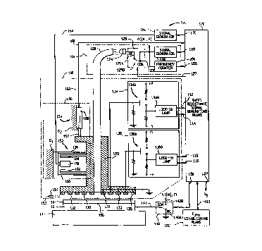
Referring now to FIG. 1, a contactless sheet resistance measurement apparatus
100 is
shown, apparatus 100 for measuring, according to a prescribed sheet resistance
model, a
sheet resistance (RS) of a desired layer 10 of a first conductivity type
formed upon an
underlying substrate 12 of an opposite conductivity type. The desired layer 10
may
comprise, for example, an ion implant layer, an epi layer, or an inverted
silicon surface.
In particular, layer 10 may comprise a lightly doped N-type ion implant layer.
Substrate
12 may comprise a P-type substrate having a prescribed substrate dopant
concentration.
A suitable vacuum chuck 14 securably holds substrate 12 in a desired position,
vacuum
chucks being well known in the art. Semiconductor substrates, ion implant
layers, epi
layers, and inverted silicon surfaces are also well known in the art, and only
briefly
discussed herein.
Apparatus 100 comprises a junction capacitance establishing means 102 for
establishing an
amount of junction capacitance of the junction between the desired layer 10
and the
underlying substrate 12. The junction capacitance establishing means 102
provides an
output signal indicative of the junction capacitance, for example, via signal
line 103.
Junction capacitance establishing means 102 of FIG . 1 may comprise a suitable
input device
for entering an input representative of a known amount of junction capacitance
of the
junction between the desired layer 10 and the underlying substrate 12. Such an
input
device may comprise a keypad or keyboard, for entering known junction
capacitance
_2146908
FI9-93-016 5
information. In instances where the junction capacitance is not known,
junction
capacitance establishing means 102 may comprise a means for measuring the
junction
capacitance of the desired layer and the underlying substrate or,
alternatively, an
electrical characteristic corresponding to the amount of junction capacitance
. For example,
such a junction capacitance establishing means may comprise any suitable
commercially
available resistivity meter, wherein the junction capacitance can be
determined as a
function of the measured resistivity, using well known methods in the art.
That is,
assuming a step junction approximation, junction capacitance is a function of
doping
concentration of the substrate which is a function of resistivity, as taught
in references
J. C. Irvin, Resistivity of Bulk Silicon and of Diffused Layers in Silicon,
Bell System Tech.
J., Vol. 41, pp. 387-410, 1962 and B. G. Streetman, Solid State Electronic
Devices, pp.
187-191, 1972. In other words, resistivity can be used to determine doping
concentration,
from which junction capacitance can be determined ~rom the doping
concentration.
A point location alternating current (AC) photovoltage generating means 104
(see FIG. 1)
is provided, means 104 for generating a point location alternating current
photovoltage
having a sinusoidal magnitude ~ M ~ and modulation frequency F at a point
location 106
(indicated in FIG. 1) between the desired layer 10 and the underlying
substrate 12. The
point location AC photovoltage is propagated radially outward from the point
location 106
laterally through the bulk of the desired layer 10 by a resistive nature of
the desired layer
10 at a corresponding attenuation and phase shift. Point location AC
photovoltage
generating means 104 further provides an output signal indicative of the AC
sinusoidal
modulation frequency F on signal line 105.
Referring again to FIG. 1, the AC point location photovoltage generating means
104
comprises any suitable light source 1.24, such as a light emitting diode (LED)
or a laser
device. Light source 124 can further comprise a light source of a wavelength
on the order
of 0. 65 to 0. 94 microns . The particular light source 124 is chosen
according to the
particular requirements of the sheet resistance measurement. For instance, the
requirements of a particular sheet resistance measurement may comprise, for
instance,
minimizing an amount of lateral scattered light and/or achieving a desired
point location
photovoltage light spot size .
Referring still to FIG. 1, light source 124 is electrically connected to a
signal generating
_214690
FI9-93-016 6
means 126 via controllable switching means 125, as shown in a normally closed
position in
FIG. 1. Controllable switching means 125 can comprise any suitable
controllable switch,
wherein a common node 123 is switchable between at least two outputs, 125A and
1258. As
shown in FIG. 1, output 125A is connected to light source 124. Switching means
125 is
controlled via a signal received on signal line 127. Light source 124 is
energized by signal
generating means 126, signal generating means 126 comprising any suitable
sinusoidal
modulation frequency signal generating means . A suitable frequency counter
128 monitors
the output signal V ( ~ M ~ ; F) of signal generating means 126 and provides a
feedback signal
indicative of modulation frequency F on signal line 105.
Point location photovoltage generating means 104 further comprises an optional
light pipe
or optical fibre 129 for directing a sinusoidal illumination of the light
source 124 to the point
location 106. In instances in which no light pipe or optical fibre are used,
light source 124
is positioned and focused by suitable means for directing its light output at
the desired
location and for generating a desired spot size. As shown in FIG. 1, the
sinusoidal
illumination of the light source 124 is directed by the light pipe 129 to form
a localized spot
125 (see FIG. 2) on a top surface of the desired layer 10. The localized light
spot 125 may
comprise a diameter on the order of 2 mm or less .
Referring again to FIG. 1, an attenuation and phase shift monitoring means 108
monitors
the attenuation and phase shift of the propagated AC photovoltage as a
function of radial
distance remote from the point location 106 . Attenuation and phase shift
monitoring means
108 provides first and second output signals, V, ( ~ V, ~ , f31 ) and Vz ( ~
VZ ~ , f32) , respectively,
indicative of a first and second monitored magnitude ~ V ~ and phase f3 at
first and second
effective radial distances, rl and r~, respectively. That is, the first output
signal,
V, ( ~ V, j , f3, ) , on signal lines 112 and 114 ( see FIG . 1 ) is
indicative of a monitored magnitude
V,~ and phase f3" respectively, at a first effective radial distance r, (see
FIG. 2) . The
second output signal, VZ( ~ Vz ~ , f32) , on signal lines 116 and 118 (see
FIG. 1) is indicative
of a monitored magnitude ~ Vz ~ and phase fit, respectively, at a second
effective radial
distance r2 (see FIG. 2) . Note that, at a minimum, the attenuation and phase
shift
monitoring means 108, and the desired layer 10 and underlying substrate 12,
should be
housed within a light-tight enclosure (not shown) to prevent undesirable photo-
induced
leakage currents during sheet resistance measurements.
214690$
~,, _
FI9-93-016 7
Referring now to FIGS. 1 and 2, attenuation and phase shift monitoring means
108
comprises first and second capacitively coupled pick-up plates, 130 and 132,
respectively,
affixed or mounted to a base member 109 (shown in cross-section in FIG. 1) by
suitable
means. First and second capacitively coupled pick-up plates, 130 and 132,
respectively,
are concentric with the localized light spot 125 and the point location 106 .
Preferably, first
and second pick-up plates, 130 and 132, comprise flat conductive metal rings
having a first
and a second effective radius, r, and r2, respectively. The second radius r2
comprises a
radius larger than the first radius r" wherein the radii are selected in
accordance with a
desired voltage characteristic of the prescribed sheet resistance model, as
will be explained
further below. As shown in FIG. 1, attenuation and phase shift monitoring
means 108
further comprises AC voltage sensing means 134 and 136, respectively, for
sensing a
magnitude and phase of an AC photovoltage capacitively coupled to the first
and second
pick-up plates 130 and 132, respectively. AC voltage sensing means 134 and 136
preferably
comprise ultra high input impedance MOSFET buffers (134A and 136A,
respectively)
connected to respective lock-in amplifiers ( 1348 and 1368) , the MOSFET
buffers minimizing
loading effects of the inner and outer pick-up plate photovoltage signals, V,
and V2,
respectively. Respective lock-in amplifiers 1348 and 1368 of voltage sensing
means 134 and
136 provide corresponding magnitude and phase output signals V, ( ( V, ~ , f31
) and Vz ( ~ VZ ~ ,
f32) , respectively for each of the first and second pick-up plates 130 and
132, respectively.
Contactless sheet resistance measurement apparatus 100 further includes a
positioning
means I50 as shown in FIG. 1. The positioning means 150 provides desired
vertical
positioning or spacing of the attenuation and phase shift monitoring means 108
between a
first position 151 and a second position 153. For .instance, first position
151 and second
position 153 may correspond to a home position and a measurement position,
respectively.
Precise vertical positioning is important for obtaining a small, repeatable,
air gap between
the capacitively coupled pick-up plates 1.30 and 1.32 and the particular wafer
under test.
For example, a desired air gap is preferably on the order of 5 mils or less
during a sheet
resistance measurement . The measurement position 153 thus preferably
corresponds to the
position at which an air gap distance of 5 mils or less between plates 130 and
132 and the
particular wafer or substrate under test is attained. With precise vertical
positioning
provided by positioning means 150, the capacitive coupling between the
capacitively
coupled pick-up plates 130 and 132 and the wafer under test can be established
to a
_2146908
FI9-93-016 8
particular value and advantageously maintained. In addition, the effective
radii of the
capacitively coupled pick-up plates 130 and 132 can also be maintained, the
effective radii
being a desired fixed value for a particular sheet resistance measurement
application, as
further explained herein below.
Positioning means 150 preferably comprises an electromechanical forcer 152, in
conjunction
with an electrical servo system 154, to raise and lower the photovoltage
monitoring means
108 in a controlled manner. The electromechanical forcer 152 can comprise a
pair of
substantially parallel flat steel flexura arms 156, an electromagnet 158, and
a pair of fixed
permanent magnets 160, all located and positioned in an arrangement such as
shown in FIG.
1. For instance, first ends of flexure arms 156 and electromagnet 158 are
mechanically
connected by suitable means (not shown) to a mechanical ground, G1. Second
ends of
flexure arms 156 are suitably mechanically connected to base member 109 of
photovoltage
monitoring means 108. Permanent magnets 160 are rigidly mounted to base member
109.
It should be noted that alternate configurations of positioning means 150 may
be used.
A signal generator 162 provides a desired signal or signals to electromagnet
158 via signal
line 164. Signal generator 162 comprises any suitable controllable signal
generator for
providing the desired signals as explained herein. Signal generator 162
provides an
appropriate signal for energizing electromagnet 158 to either force the fixed
magnets 160
up or down, thereby effectively raising or lowering photovoltage monitoring
means 108 up
or down. In this regard, a prescribed controlled amount of direct (DC) current
provided
to electromagnet 158 causes flexure arms 156 to flex in a controlled manner to
thereby
position photovoltage monitoring means 108 in a desired position, while
further maintaining
voltage pick-up plates 130 and 132 substantially parallel to the surface of
the wafer under
test. Signal generator 162 further provides an appropriate alternating current
AC signal
for energizing electromagnet 158 to cause photovoltage monitoring means 108 to
vibrate in
a controlled manner, to be explained further herein below with respect to
operation of the
present invention .
Feedback for servo system 154 is provided by a linear variable differential
transformer
(LVDT) 166, which outputs a position dependent signal on signal line 168. LVDT
166
comprises any suitable linear variable differential transformer. LVDT 166 is
mechanically
_214F9~
FI9-93-OI6 9
grounded at a mechanical ground GZ by suitable means (not shown) so that
plunger 167 of
LVDT 166 is in suitable contact with base member 109 of attenuation and phase
shift
monitoring means 108. Movement of means 108 up or down results in a
corresponding
movement of plunger 167 up or down, whereby LVDT 166 provides a corresponding
position
dependent output signal on signal line 168.
Servo system 154 facilitates calibration of positioning means 150, i. e. , for
establishing
prescribed amounts of DC current to be provided by signal generator 162 to
electromagnet
158, in conjunction with position dependent output signal information provided
on signal
line 168, thereby enabling accurate automated control of positioning means 150
for desired
positioning of attenuation and phase shift monitoring means 108 (e. g. ,
between the first
position 151 and the second position 153, or an alternate position) during
operation o~ sheet
resistance measurement apparatus 100. Appropriate calibration of positioning
means 150
includes calibration of the positioning of attenuation and phase shift
monitoring means 108
with respect to the surface of the desired layer 10 for establishing a desired
air-gap
therebetween on the order of 5 mils or less, as previously noted. Positioning
means 150
may also be responsive to a prescribed change in a calibration attenuation and
phase shift
for establishing a desired air gap corresponding to the measurement position.
Positioning
means 150 further advantageously enables means 108 to be placed in a raised
position while
enabling substrate 12 to be mounted upon vacuum chuck 14 easily, or enables
substrate 12
to be positioned under monitoring means 108 without damage to the substrate 12
or to the
first and second pick-up plates 130 and 1.32, respectively.
Sheet resistance measurement apparatus 100 further comprises a sheet
resistance RS signal
generating means i20 (See FIG. l.) . Sheet resistance RS signal generating
means 120 may
comprise for example, a computer and associated interface circuitry, discrete
circuitry,
or the like, for receiving and providing signals as outlined herein below and
for performing
prescribed functions . Preferably, sheet resistance generating means 120
comprises a
computer and associated interface circuitry, computers and associated
interface circuitry
being well known in the art and only briefly discussed herein, the computer
further being
programmed by known techniques for performing desired funeti:ons as described
herein
below also.
Sheet resistance signal generating means 120 is connected to signal line 103
for receiving
.. 214soos
FI9-93-016 10
a junction capacitance C~t~ signal from junction capacitance establishing
means 102 . Means
120 is connected to signal line 105 for receiving a signal representative of
the AC sinusoidal
modulation frequency F of point location AC photovoltage generating means 104.
Means 120
provides appropriate control signals to AC photovoltage generating means 104
via signal
lines 127 and 128 for controlling controllable switching means 125 and signal
generator 126,
respectively, in a desired manner as will be explained further herein below
with respect
to operation of the invention .
Sheet resistance signal generating means 120 is also connected to attenuation
and phase
shift monitoring means 108, and in particular, to signal lines 112 and 114 0~
FIG. 1 for
receiving magnitude ~ V, ~ and phase f3" respectively, of the first output
signal, V, ( ~ V, ~ ,
13,) . Furthermore, sheet resistance output signal generating means 120 is
connected to
signal lines 116 and 118 of FIG. 1 for receiving magnitude ~ V~ ~ and phase
13z, respectively,
of the second output signal, V2( ~ V~ ~ , fy) .
Sheet resistance signal generating means 120 is further connected to
positioning means 150
via appropriate connections, for example, to signal line 168 for receiving
position
dependent output signal information from LVDT 166. Means 120 further provides
an
appropriate control signal to positioning means 150 via signal line 170 for
controlling
controllable signal generator 162 in a desired manner as will be explained
further herein
below with respect to operation of the invention.
Still further, sheet resistance signal generating means 120 provides an
appropriate control
signal to a controllable switching means 140 via signal line 138 for
controlling controllable
switching means 140 in a desired manner as will be explained further herein
below with
respect to operation of the invention . Controllable switch means 140 can
comprise any
suitable controllable switch, wherein a common node 141 is switchable between
at least two
inputs. Preferably, a first input 140A is suitably connected to ground
potential and a
second input 1408 is suitably connected to receive voltage signal V ( ( M ~ ,
F) of signal
generating means 126.
In response to the junction capacitance C~t~, the AC sinusoidal frequency F,
and the first
and second attenuation and phase shift signals V, ( I V, ~ , f3, ) and VZ ( ~
VZ ~ , f3z) , respectively,
and further in accordance with the prescribed sheet resistance model, sheet
resistance
~14~9Q~
FI9-93-016 11
signal generating means 120 generates an output signal indicative of a sheet
resistance RS
of the desired layer 10. Such an output signal may be provided on an output
signal line
122, for example. Similarly, the output signal may likewise be printed out via
a printer
device (not shown) or displayed upon a display device (not shown) .
In conjunction with the present invention and as utilized in accordance with
the present
invention, the prescribed sheet resistance model will n.ow be described in
detail. The
prescribed sheet resistance model has been derived based upon considering the
desired
layer of interest 10 to be a resistive sheet with a distributed P-N junction
capacitance
between the layer 10 and the underlying opposite conductivity substrate 12 .
The resistive
layer 10 and its associated P-N junction are treated as a small signal
alternating-current
(AC) distributed resistance-capacitance (R-C) transmission line network. R-C
distributed networks are well known in the art and only briefly discussed
herein. From a
characterization of this R-C distributed network in terms of an AC attenuation
and an AC
phase shift as a function of distance, in addition to knowing an established
junction
capacitance, the sheet resistance (RS) of interest is determined. That is, the
sheet
resistance, RS, (ohms/square) of th.e desired layer 10 and the junction
capacitance, C~t~,
(farads/cm2) as well as a leakage conductance, G, (mhos/cm2) , between the
desired layer
10 and the underlying bulk silicon 12 form a distributed R-C-G circuit. Vo is
an AC
photovoltage induced by a localized light spot, with sinusoidal modulation
frequency, F,
variation in illumination intensity. V, and V~ are the resultant attenuated AC
photovoltages
at effective radial distances, r, and r2, respectively, from the centre of the
light spot. The
ratio of attenuated voltages, VZ/V" is then a function, as expressed by f (R,
C, G, r" r2,
F) , which yields a calculable value for the sheet resistance, RS, of
interest. The desired
model is thus expressed as:
V~/V, = Ko(Kr~)/Ko(Kr,),
wherein Ko(Kr) is amodified zero order Bessel series of the second kind, and K
is a complex
number, and r is a radial distance. 'The function Ko(Kr) can be expressed as:
Ko(Kr) = A + jl3 = (Ko(Kr) ~e'° .
Complex number K can be expressed as:
2146908
FI9-93-016 12
K=E+jF= IKIem~
wherein the value of K is made up characteristic parameters P and g, which are
expressed
as:
g = G/ ( 2~rFC ) , and
P = (~rFRC)~ cm'.
In view of the above, the expression for sheet resistance model VZ/V, may be
rewritten as
follows
I VZ/V1 I ego = I Ke(Kr~) I eio2/ I Ko(Kr,) I ejo~ = f(p~ g)
wherein P and g are expressed as above, and
~ = f32 - f3, radians .
In connection with the sheet resistance model, suitable values for radial
distances rl and
r2 and a small-signal magnitude of VZ/V, are selected, thereby establishing
prescribed
boundary conditions . Selection of the specific values ~or radial distances r,
and r2 and the
small-signal magnitude of VZ/V, is based upon compromises between desired
spatial
resolution, system noise, measurement accuracy, desired repeatability, etc. ,
according
to the particular requirements of the sheet resistance measurement
application. For
instance, one boundary condition of the sheet resistance model may require
attenuation of
the photovoltage to zero volts over a prescribed radius, for example, two (2)
cm, as shown
by radius r3 in FIG. 2. In addition, to achieve a desired small-signal
magnitude of VZ/V"
the small-signal magnitude of V.,/V, is forced during sheet resistance
measurements by
adjusting the sinusoidal modulation frequency, F, of the light source 124. The
small-signal
magnitude of VZ/V, is selected to be on the order of 1 mV or less, to thereby
maintain the
excitation photovoltage at such a level so that undesired voltage effects upon
the substrate
during the sheet resistance measurement are substantially reduced or
eliminated. The
magnitude of VZ/Vl is thereby forced so as to fit prescribed boundary
conditions of the
sheet resistance model according to the present invention.
Also in conjunction with the above discussion, sheet resistance RS signal
generating means
,, 21469Q8
FI9-93-016 13
120 further comprises a adjustment means for adjusting the modulation
frequency F to
achieve a prescribed change in attenuation monitored by said attenuation and
phase shift
monitoring means 108 between the first and second radial distances, rl and r2,
respectively. Preferably, sheet resistance signal generating means 120
comprises a means
for: i) controlling signal generating means 126 to provide an AC voltage
signal at a
modulation frequency F (wherein an initial modulation frequency F - FINIT is
used to begin
this portion of process) , thereby exciting light source 124 for creating a
point location AC
photovoltage between the desired layer 10 and the underlying substrate 12; ii)
monitoring
a magnitude ~ V, ~ and phase f3, at radius r, and a magnitude ~ Vz ( and phase
f3z at radius r2;
and iii) adjusting the frequency F until the ratio of monitored ~ V, ~ to
monitored I VZ ~ is
approximately 4:1 in accordance with the prescribed sheet resistance model to
within a
prescribed range or tolerance. In this manner, modulation frequency F is
adjusted until
the monitored voltage ~ VZ ~ at radius r2 is approximately one-quarter ( 1/4)
of the monitored
voltage ~ V, ~ at radius r, . The adjusted frequency F is then used for the
subsequent sheet
resistance determination of the desired layer 10, as will be further explained
herein below.
Furthermore, adjustment of the modulation frequency F in the above described
manner
establishes the spot size 125 and results in the voltage at radius r3 (i. e. ,
a desired
boundary condition) being approximately zero volts .
In conjunction with adjustment of modulation frequency F as discussed above, a
voltage
measurement signal calibration can be performed also. Voltage measurement
signal
calibration is accomplished via sheet resistance signal. generating means 120
such that, at
any modulation frequency F, any differential variations in magnitude or phase
shift
between the outputs of voltage sensing means 134 and 136 may be compensated
for, as
appropriate. More particularly, for achieving a desired voltage measurement
signal
calibration, sheet resistance RS signal generating means 120 is operative via
signal line 138
for selectively connecting signal generating means 126 (i . a . , signal V ( ~
M ~ , F) ) to substrate
12 via controllable switch means 140 of FIG. 1 during a voltage measurement
signal
calibration. In other words, controllable switch 140 is controlled via an
appropriate signal
provided upon signal line 138 for switching the connection of common terminal
141 from 140A
to I40H. In addition, during voltage measurement signal calibration, sheet
resistance RS
signal generating means 120 is operative via signal line 127 for selectively
disconnecting
signal generating means 126 from light source 124 via controllable switch
means 125 of FIG.
1. That is, controllable switch 125 is controlled via an appropriate signal
provided upon
_m4s~os
FI9-93-016 14
signal line 127 for switching the connection of common terminal 123 from 125A
to 1258. During
a signal calibration operation, the magnitude and phase output signals on
signal lines 112,
114 and 116, 118 corresponding to V, and Vz, respectively, are compared with
each other
using the output of signal generator 126 as a reference signal, i. a . , V ( ~
M ~ , F) .
Appropriate adjustments to the gains of the voltage sensing means 134 and 136
may be made
or appropriate calibration compensation values corresponding to the particular
modulation
frequency F may be established and stored for use by sheet resistance signal
generating
means 120. Signal calibration is preferably performed at each modulation
frequency F.
Such a voltage signal calibration by means 120 advantageously assists in
establishing a
desired modulation frequency F for the point location AC photovoltage
generating means
104 according to the particular desired layer 10 and underlying substrate 12
being tested.
In continuation of the above discussion with respect to determination of the
sheet
resistance according to the prescribed sheet resistance model, sheet
resistance RS signal
generating means 120 further comprises a means for: i) generating an actual
magnitude
V,/Vz ~ A~t"~1 and phase ~A~t~A~ (wherein ~A~t~eW- 8z -Ji, ) according to the
prescribed sheet
resistance model, the sheet resistance model being based upon the propagation
of the AC
photovoltage as a function of radial distance remote from the point location,
the prescribed
model further comprising first and second prescribed characteristic parameters
P and g,
respectively; ii) estimating the first characteristic parameter P and the
second
characteristic parameter g, the estimated first characteristic parameter PEST
and the
estimated second characteristic parameter gEST being updatable in a prescribed
manner; iii)
generating a theoretical magnitude ~ 'J,/Vz ~ THEO and phase ~THEO according
to the prescribed
sheet resistance model, the estimated First characteristic parameter PEST, and
the estimated
second characteristic parameter gE~T; iv) comparing the theoretical magnitude
and phase
( ~ V,/V2 J THEOJ ~ THEOi .to the actual magnitude and phase ( ~ V,/V~ ~
A~t~al, ~A~E~~,) and, upon the
theoretical magnitude and phase being outside a prescribed range of the actual
magnitude
and phase, iteratively updating the estimated first and second characteristic
parameters
and repeating iii) and iv) ; and v) using a most recent value of the estimated
first
characteristic parameter PEST, the junction capacitance CST", and the
modulation frequency
F to determine the sheet resistance RS in accordance with the prescribed sheet
resistance
model .
C~, 21~~~~8
FI9-93-016 15
Operation of the present invention will now further be explained with
reference to the
apparatus figure (FIG. 1) and flow diagrams (FIGS . 3-5) . Corresponding to
the beginning
of a sheet resistance measurement, as indicated by Step 200 of FIG. 3, a
semiconductor
substrate 12 of a first conductivity type having a desired layer 10 of an
opposite
conductivity type thereon, is securably mounted upon wafer chuck 14 (FIG. 1) .
Sheet
resistance of the desired layer 10 is then determined using the apparatus and
method of the
present invention. In step 202 of FIG. 3, an amount of junction capacitance
Cat" is
established via the junction capacitance establishing means 102. A junction
capacitance
signal is provided to sheet resistance signal generating means 120 via signal
line 103 (FIG.
1) . In the instance wherein junction capacitance establishing means comprises
a keyboard,
a known junction capacitance value may simply be entered via the keyboard . In
the instance
wherein junction capacitance establishing means comprises a measurement
device, a
suitable measurement is made according to the particular requirements of the
measurement
device whereby the output signal representative of a measured value of
junction
capacitance, or some electrical characteristic proportional to junction
capacitance, is
provided via signal line 103 to sheet resistance signal generating means 120.
Sheet
resistance signal generating means 120 maintains or stores the established
value of junction
capacitance for subsequent use, as will be further described.
In preparation for making a Sheet resistance measurement of the desired layer,
a desired
measurement spacing is established for the attenuation and phase shift
monitoring means
108 (FIG. 1) as indicated in Step 204 (FIG. 3) . In particular, signal
generating means 120
(FIG. 1) provides an appropriate control signal to signal generator 162,
wherein signal
generator 162 provides a corresponding DC signal along line 164 to the
electromagnetic
forcer 152. Attenuation and phase shift monitoring means 108 then moves from a
first
position 151 to a second position 153, the second position 153 corresponding
to a desired
measurement spacing. Feedback control for the spacing is provided via the
position
dependent output signal provided on signal line 168 from LVDT 166.
In the next step (Step 206 of FIG. 3), modulation frequency F of signal
generating means
126 is adjusted by sheet resistance signal generating means 120 (FIG. 1) .
Adjustment of
modulation frequency F is performed to achieve the prescribed change in
attenuation
monitored by said attenuation and phase shift monitoring means 108 between the
first and
second radial distances, r, and r~, respectively. Referring now to FIG. 4, in
Step 2061,
",, ~ 2146~~~
FI9-93-016 16
the modulation frequency F is set to an initial value F,NIT ~ In Step 2062,
sheet resistance
signal generating means 120 calibrates the magnitude and phase voltage signal
outputs of
V, and VZ using signal V ( ( M~ , F) . As discussed above, voltage measurement
signal
calibration is accomplished via sheet resistance signal generating means 120
such that, at
a particular modulation frequency F, any differential variations in magnitude
or phase shift
between the outputs of voltage sensing means 134 and. 136 may be compensated
for, as
appropriate . A first calibration of the magnitude and phase outputs occurs at
the
frequency F equal to FI"IT.
Referring still to FIG. 4, in Step 2063, sheet resistance signal generating
means 120 is
operative to generate a point location photovoltage. With reference now to
FIG. 1, sheet
resistance signal generating means 120 sends an appropriate signal on line 138
to control
switching means 140 for electrically grounding substrate 12 with respect to an
alternating
current (AC) potential. Sheet resistance signal generating means 120
thereafter sends a
signal via signal line 126A for instructing signal generating means 126 to
provide an AC
voltage signal V ( ~ M ~ , F) at modulation frequency F, thereby exciting
light source 124 for
creating a point location AC photovoltage between the desired layer 10 and the
underlying
substrate 12. The frequency F is monitored via frequency counter 128 on signal
line 105.
The excitation light is directed to the desired layer 10 and the underlying
substrate 12 via
light pipe 129 at point location 106, thereby forming a localized light spot
of a diameter 125
(See FIG. 2) on a top surface of desired layer 1Ø A point location
sinusoidal AC
photovoltage is thereby created at an interface between the desired layer 10
and the
underlying substrate 12, the photovoltage propagating radially outward . In
other words,
the photovoltage, having a sinusoidal magnitude and frequency, propagates
radially
outward from the point location 106 along the desired layer 1.0 by the
resistive nature
thereof . The propagation of the photovoltage is further characterized by an
attenuation
and phase shift.
Referring again to FIG. 4, in Step 2064, sheet resistance signal generating
means 120
monitor. s the magnitude ~ VI ~ and phase f3, at radius r, and the magnitude ~
VZ ~ and phase f3z
at radius r2, via the output signals of attenuation. and phase shift
monitoring means 108
(FIG. 1) . That is, the attenuation and phase shift of the propagated AC
photovoltage as
a function of radial distance is monitored by monitoring means 108. Means 108
monitors the
magnitude and phase of the photovoltage at first and second radial distances,
rl and r2, via
,, X146908
FI9-93-016 17
capacitively coupled pick-up plates 130 and 132, respectively. Voltage signals
sensed by
the pick-up plates are input into voltage sensing means 134 and 136,
respectively.
Magnitude and phase signals, V, ( ~ V, ~ , f3, ) and V~ ( ~ V2 ~ , f32 ) , are
provided on respective
output signal lines 112, 114 and 116, 118. The output signals 112, 114 and
116, and 118 are
thus received by sheet resistance signal generating means 120.
During the monitoring of attenuation and phase shift at the first and second
radial
distances, an AC signal (on the order of approximately 27 Hz) is applied to
electromagnet
158 via signal generator 162, as controlled by means 120 via signal line 170.
The AC signal
applied to electromagnet 158 results in a slight vibrating of the base member
109 and the
corresponding capacitively coupled pick-up plates 130 and 132. Vibrating of
the
attenuation and phase shift monitoring means 108 in this manner creates a
Kelvin probe
type measurement. Monitoring of semiconductor wafer surface voltages using
Kelvin probe
apparatus for Kelvin probe type measurements is well known in the art, and
thus not
discussed in great detail herein. With reference to the present invention,
such a Kelvin
probe type measurement enables the measuring a DC voltage component imposed
upon the
junction formed by the desired layer 10 and the underlying substrate 12. The
DC voltage
component imposed upon the junction results from the application of the AC
photovoltage,
thereby introducing an undesirable error component into the sheet resistance
ZO measurement. Measurement of the DC voltage component enables such
undesirable errors
to be compensated for in an appropriate manner.
To further ensure the integrity of the voltages sensed by th.e capacitively
coupled pick-up
plates 130 and 132, and to minimize the potential for undesirable cross-
coupling between
the pick-up plates, grounded plates 131, 133, and 135 are provided (see FIG.
1) .
Grounded plates 131, 133, and 135 preferably comprise flat conductive rings of
suitable
dimensions affixed or mounted to base member 109 by suitable means and
connected to a
ground potential for effectively shielding plates 130 and 132.
Having now monitored the photovoltage attenuation and phase at first and
second radial
distances, we now turn once again to FIG. 4. In Step 2065, means 120
determines whether
the ratio of the magnitude ~ V, ~ to magnitude ~ VZ ~ is approximately 4:1
within a prescribed
range. If the ratio is outside the prescribed range, means 120 adjusts the
frequency F in
a prescribed manner in Step 2066, and then repeats steps beginning with Step
2062.
,~ _2146908
FI9-93-016 18
Adjustment of frequency F is made as appropriate, that is, in a prescribed
manner whereby
increasing F to a higher frequency decreases the radial distance in which the
photovoltage
attenuates to zero, and whereby decreasing F to a lower frequency increases
the radial
distance in which the photovoltage attenuates to zero. If the ratio of
monitored , V, ~ to
monitored ~ VZ ~ is approximately 4:1 in accordance with the prescribed sheet
resistance
model within a prescribed range or tolerance, then adjustment of the
modulation frequency
F is completed for the particular desired layer 10 and underlying substrate
12. In this
manner, the magnitude of VZ/V, is forced to a particular value according to
the sheet
resistance model. Alternatively, modulation frequency F is adjusted until the
monitored
voltage ~ VZ ~ at radius rZ is approximately one-quarter ( 1/4) of the
monitored voltage , V1
at radius r, . The adjusted frequency F, in addition to the actual monitored
magnitude and
phase of Vl and VZ (i. e. , for determination of I VZ/V, ~
A~t~Ale'~A°t°al) are then used for the
subsequent sheet resistance determination of the desired layer 10, as will be
further
explained herein below.
It should be noted that the amount of junction capacitance C~t~ may
alternatively be
established via the junction capacitance establishing means 102 subsequent to
the
adjustment of frequency F. That is, Step 202 may be occur after Step 206.
We now turn to FIGS. 3 and 5, where in Step 208, the present invention
determines
theoretical values for P and g, such that the theoretical magnitude and phase
of VZ/V, are
substantially equal to the actual forced magnitude and measured phase of
Vz/V1. That is,
successive approximation values of P and g, as further discussed herein below,
are used
to generate corresponding theoretical magnitude ~ Vz/V, ~ and phase ~ values
until a
theoretical magnitude ( VZ/V1 ~ and phase ~ value are substantially equal to
the forced actual
magnitude ~ VZ/V, ~ A~t~~~ and phase ~A~t~m within a prescribed range or
tolerance . Criteria for
establishing at what point the theoretical magnitude and phase of VZ/V, are
substantially
equal to the forced actual magnitude and phase of V~/V, may be established in
accordance
with the desired accuracy of the sheet resistance measurement. Upon obtaining
the value
for P and g for which the corresponding theoretical magnitude ~ VZ/V, ~ and
phase
substantially equals the forced actual magnitude ~ VZ/V, ~ A~t~e~ and phase
~A~t~a~, the sheet
resistance, RS, of interest is then determined according to the sheet
resistance model based
upon characteristic parameter P, and further in view of frequency F and
junction
capacitance C~t~ . Recall that F is the adjusted sinusoidal modulation
illumination frequency
2~.469Q8
FI9-93-016 19
that was needed to force the desired small-signal magnitude of V2/V1 and C~t~
is the P-N
junction capacitance .
Turning now to FIG. 5, in step 2081, the forced actual magnitude ~ VZ/V, ~
A~t~e~ and phase
~A~t~e~ are determined by sheet resistance signal generating means 120 based
upon inputs
received on signal lines 112, 114 and 116, 118 at the adjusted frequency F as
discussed
above. That is, sheet resistance RS signal generating means 120 generates an
actual
magnitude ~ V,/VZ ~ A~t~e~ and phase ~A~t~e~ according to the prescribed sheet
resistance model,
wherein the sheet resistance model is based upon the propagation of the AC
photovoltage
as a function of radial distance remote from the point location. In Step 2082,
recalling above
that according to the prescribed model, the magnitude ~ V,/VZ ~ and phase ~
are further a
function of first and second prescribed characteristic parameters P and g,
sheet resistance
RS signal generating means 120 estimates the first characteristic parameter
PEST and the
second characteristic parameter gEST. That is, the estimated first
characteristic parameter
PEST is set to an initial estimated value PINIT and the estimated second
characteristic
parameter gESr is set to an initial estimated value g,NIT ~ Fu.rthermore, the
estimated first
characteristic parameter PEST and the estimated second characteristic
parameter gEST are
updatable in a prescribed manner, such as, according to a suitable
extrapolation method
or other method for approximating such parameters, to be discussed further
herein below.
Referring still to FIG. 5, in Step 2083, sheet resistance signal generating
means 120
generates a theoretical magnitude ~ VZ/V, ~ Theo and phase ~Theo according to
the prescribed
sheet resistance model, the estimated first characteristic parameter PEST, and
the estimated
second characteristic parameter gE~T . Upon obtaining both the actual and
theoretical
magnitude and phases, means 120 compares the theoretical magnitude ~ V,/V2 ~
THEO and phase
~T"~o to the actual magnitude ) V,/Vz ~ AcFual and phase ~A~t~al in Step 2084.
If a result of the comparison in Step 2084 indicates that the theoretical
magnitude and phase
is not substantially equal to the actual magnitude and phase within a
prescribed range,
means 120 iteratively updates the estimated first and second characteristic
parameters PEST
and gES, in Step 2085, and repeats Steps 2083 and 2084. Preferably,
characteristic
parameters P and g are updatable by a successive approximation method, the
method
determining updated values for P and g as briefly described in the following.
Since the
214690$
FI9-93-016 20
theoretical magnitude ~ Vz/V, ~ and phase ~ are both functions of P and g,
their relative
sensitivities to P and g are used to select successive estimates for P and g.
For example,
if a fifteen percent ( 15%) change would be needed to make the theoretical
value of ~ VZ/V,
equal to the actual value of I V~/V, ~ and the theoretical value of ~ VZ/V, ~
happened to be
equally sensitive to changes in P and g, then P and g would both be
incremented by seven
and a half percent ('7. 5°s) (i. e. , 15°~ divided in half ) .
On the other hand, if the theoretical
value of ( VZ/V, ~ happened to be twice as sensitive to changes in P than to
changes in g,
then P would be incremented by ten percent (10°x) and g would be
incremented by five
percent (5°s) . Sensitivities of the theoretical value of I VZ/V, ~ and
phase ~ to P and g for
this successive approximation method. are determined by the use of partial
derivatives
which are well known in the art .
If a result of the comparison in Step 2084 indicates the theoretical magnitude
and phase to
be substantially equal to the actual magnitude and phase within a prescribed
range, then
updating of first and second characteristic parameters P and g, respectively,
is completed .
Means 120 thereafter in Step 210 of FIG. 3 utilizes the most recent value of
the estimated
first characteristic parameter PEST, the junction capacitance C~t~, and the
adjusted
frequency F to determine the sheet resistance RS in accordance with the
prescribed sheet
resistance model (i.e. , in accord with the expression P = {~rFRC)' cm ') .
Thus, sheet resistance signal generating means 120 is responsive to the
junction
capacitance C~t~ signal on signal line 103, the adjusted AC sinusoidal
frequency F signal on
signal line 105, and the first and second attenuation and phase shift signals
on signal lines
112, 114 and 116, 118 for generating an output signal indicative of a sheet
resistance RS of
the desired layer 10 according to the sheet resistance model, where R is the
sheet
resistance parameter of interest.
In an alternate embodiment as shown in FIG . 6, the invention is substantially
similar to that
described above with reference to FIGS . 1-5, however, with the following
differences .
Wafer chuck 14 is mounted upon a suitable slide track 16, utilized for
transporting chuck
14 between first and second positions, indicated by numerals 10 and 20,
respectively. Slide
track 16 is connected to sheet resistance signal generating means 120 via
control signal line
18. The first position 20 is representative of the wafer chuck 14 being in a
sheet resistance
measurement position and the second position 30 corresponds to a second
measurement
~", _ 2146998
FI9-93-016 21
position, such as, a junction capacitance measurement position, for instance.
In this later
case, a junction capacitance measurement means 102A for measuring a
characteristic of
desired layer 10 on substrate 12 representative of junction capacitance is
shown positioned
above second measurement position 30. Junction capacitance measurement means
102A is
connected to sheet resistance signal generating means 120 via signal line
103A. Operation
of sheet resistance measurement apparatus 100 of FIG. 6 operates substantially
similar to
that of the preferred embodiment. Alternate measurement means may be provided
at
measurement position 30, for example, a four-point probe for use in comparison
measurement testing or other forms of testing, wherein junction capacitance
establishing
means 102 could be as described with respect to the preferred embodiment as
shown in FIG.
1.
There has thus been shown a contactless sheet resistance measurement apparatus
and
method of measuring the sheet resistance of a desired layer having a first
conductivity type
over an underlying substrate having an. opposite conductivity type. The
apparatus and
method of the present invention are well suited for providing a desired highly
accurate and
repeatable measurement of sheet resistance RS of a desired layer. The present
invention
further provides a number of other advantages, relative to the conventional
four point
probe and metal-oxide-semiconductor (MOS ) methods . For example, in contrast
to the four
point probe method, the screen oxide layer that is normally grown on a wafer,
prior to ion
implantation, does not have to be stripped, since the present invention is
contactless .
This yields far more accurate RS values, due to avoiding electrical alteration
of the surface
of the implant layer that would otherwise occur from chemically stripping the
screen oxide .
Furthermore, in contrast to the MOS method, the present invention is capable
of
measurements above a 5E12 implant dose range and does not require the
expensive, time
consuming and destructive processing needed to form electrodes for capacitive-
voltage
testing. The ability to correct for measurement error, due to leakage of the P-
N junction
between the implant layer and the underlying opposite conductivity substrate,
is an
additional advantage over conventional four point probe methods .
While the invention has been particularly shown and described with reference
to the
preferred embodiment thereof, it will be understood by those skilled in the
art that various
changes in form and detail may be made therein without departing from the
spirit and scope
of the invention. For example, adjusting of the sinusoidal pulsing frequency
of the light
2146908
FI9-93-016 22
source 124 in order to force a desired ~ V~/V, ~ ratio can be accomplished by
having a local
computer make successive frequency adjustments (as in the preferred
embodiment) or by
using an electronic servo system. For the case of a servo system, a feedback-
controlled,
voltage to frequency converter could automatically perform the frequency
adjustment.