Note : Les descriptions sont présentées dans la langue officielle dans laquelle elles ont été soumises.
X14"121
APPARATUS FOR SECURING THE INTEGRITY OF
A FUNCTTONING SYSTEM
BACRGROtTND OF THE INVENTION
The present invention relates generally to
apparatus for securing the integrity of a system,
and more particularly to electronic apparatus having
a primary device such as a secure microprocessor for
performing a function and a secondary device adapted
for simulating that function and securing the
l0 function of the primary device.
The pirating or unauthorized interception of
one's property can be a substantial threat to, e.g.,
a producer of services. For example, the
unauthorized receipt of transmitted television
programming incurs a substantial cost in lost
profits to a satellite television or cable
television (CATV) company. To protect against the
pirating of a transmitted digital signal, encrypting
devices using encryption codes have been developed
for digital encryption of the signal. However,
pirates can sometimes break the encryption by, e.g.,
attacking the hardware which performs the encryption
function.
One way that encryption hardware has been
compromised by intruders is via high-speed clock
pulsing attacks on very large scale integration
(VLSI) microprocessor circuitry used by the
encryptor. A certain common aspect of VLSI
microprocessor circuitry has been suspected of being
2
vulnerable to these high-speed attacks. This aspect
is known as "precharge" and refers to a minimal-area
circuit design technique that connects data busses
and shared control lines inside a VLSI
microprocessor. It is believed that high-speed
clock pulsing affects the operation of this type of
circuitry.
Precharge acts like a time-sliced wired-OR bus
for data. During some initialization time period,
the data line is forced to a logic state that is
opposite to the data state put onto the line by the
multiple drivers used. This logic state is usually
a one, or high voltage level. Following this
initialization or precharge period, one of many
driving data sources is allowed to pull the line low
if a zero is the data bit state to be placed on the
bus. Of course, there is no need for a data source
to drive a logic one onto the line if it is
precharged high, since the line has already been
initialized into that state.
One way to detect an intruder involves
monitoring the behavior of the '°primary" circuit to
be protected, e.g., a microprocessor, during this
precharge period. If the primary circuit should be
at a particular state, e.g., high or low, and it is
not, then an attack may be occurring. However, it
is very difficult to detect errant behavior of a
complex device such as a microprocessor without
2~~721~
3
adding a tremendous amount of dedicated circuitry
fox this purpose.
Accordingly, it would be advantageous to
provide a relatively non-complex means that is
useful fox detecting the errant behavior of a
primary device. It would also be advantageous to
provide a low-cost means for detecting errant
behavior. It would further be advantageous to
detect an intruder attempting to withdraw
information contained in a device and, in response,
to secure the information and thereby prevent its
loss. .
The present invention provides an apparatus
having the aforementioned advantages. In
particular, the apparatus of the present invention
provides a "secondary" device which simulates the
vulnerability associated with a function of a
primary device. Upon a breach of the simulated
vulnerability provided by the secondary device, the
latter will secure the primary device. Thus, a
relatively inexpensive and non-complex apparatus is
provided for securing a complex functioning system.
2.~4~2.~~
4
- SUMMARY OF THE INVENTION
In accordance with the present invention, ,
apparatus is provided for securing the integrity of
a functioning system. The apparatus comprises a
primary device, e.g. a processor, for performing a .
function and has a first associated vulnerability.
A secondary device is provided which has a second
vulnerability that emulates (e. g., is virtually
identical to) the first vulnerability of the primary
device. The secondary device is adapted to secure
the function performed by the primary device in
response to activity breaching the second
vulnerability.
The primary device may comprise a first circuit
means having a first input means. In such an
embodiment, the secondary device comprises second
circuit means having second input means for
receiving substantially similar input as that input
to the first input means. The second circuit means
also.has an output connected to, e.g., a reset of
the first circuit means for securing, or resetting,
the first circuit means.
In a first illustrated embodiment, the first
circuit means includes at least one circuit element
adapted to be precharged to a first state via the
first input means. The second circuit means is
adapted to simulate the precharge to the first state
via the second input means. The second circuit
~~4721
means~further includes means for determining whether
the simulated precharged state equals either a
"normal" state or an °'attack detected" state. The
second circuit means secures the function performed
5 by the first circuit means in response to a finding
by the determining means that the simulated
precharged state equals the attack detected state.
For example, where the primary device includes a
processor for decrypting a signal, the decryption
codes used by the processor may be secured by
erasing them.
In another embodiment, the vulnerability of the
primary device involves the transfer of information
into and out of a storage means. In this situation,
the first circuit means comprises storage means and
first transfer means for transferring the
information processed by the function into and out
of the storage means. To simulate this
vulnerability, the second circuit means includes
second transfer means for transferring a known value
in response to the transfer of information by the
first transfer means. Means are provided for
verifying that the known value has been validly
transferred. Additionally, the securing of the
function would be accomplished by suspending the
transfer of information to or from the primary
device. Another possible way to secure the function
would be to reset a register utilized by the
function.
2.~472~.
6
In another illustrated embodiment, the first
circuit means comprises first means for addressing a
memory and the second circuit means includes second
means for addressing a memory using a relative jump.
Also provided are means for verifying that a correct
relative jump has been effected.
2-~~72.1~
' BRIEF DESCRIPTION OF THE DRAWTNGS
Figure 1 is a block diagram of a first
embodiment a device fox securing the integrity
of of
a functioning system in accordance with the present
invention;
Figure 2 is a block diagram of a simulator
for
use in the
first embodiment
of the present
invention;
Figure 3 is a timing diagram showing a clock
cycle and resultant
effect of
the time constant
during precharge
of a primary
device;
Figure 4 is a more detailed block diagram
of
the device Figure 2;
of
Figure 5 is a timing diagram for the device
of
Figure 2;
Figure 6 is a circuit diagram of a detector
for
simulating electronic storage cell which is
an
charged high from a clock pulse;
Figure 7 is a circuit diagram of a detector
for
simulating electronic storage cell which is
an
charged high from an inversion of the clock
pulse;
Figure 8 is a circuit diagram of a detector
for
simulating electronic storage cell which is
an
charged low
from a clock
pulse;
Figure 9 is a circuit diagram of a detector
for
simulating electronic storage cell which is
an
. charged low rom an inversion of the clock pulse;
f
2~~~21~
8
Figure 10 is a block diagram of another
embodiment of a device for securing a functioning
system in accordance with the present invention; and
Figure 11 is a block diagram of yet another
embodiment of a device for securing a functioning
system in accordance with the present invention.
2~4~21~
9
DETAILED DESCRIPTION OF THE INVENTION
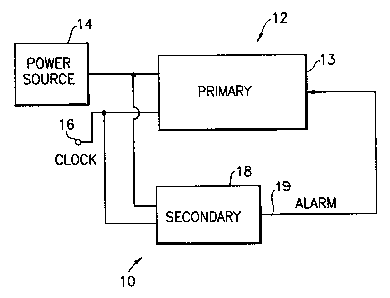
Figure 1 illustrates a first embodiment of an
apparatus generally designated 10 for securing the
integrity of a functioning primary device or system
shown generally at 12. It will be appreciated that
the primary system 12 may be any system which
performs a function, such as an electronic circuit.
It will also be appreciated that the function
performed by the primary system 12 may vary widely,
and is vulnerable to loss or interference either
from inside or outside the primary system. The
primary system 12 may comprise, for example, a
secure microprocessor used in conjunction with the
decryption of an encrypted signal.
The primary device 12 illustrated in Figure 1
includes a processor 13 which is coupled to a
suitable power source 14, and receives a clock
signal from a clocking means via terminal 16. The
clocking means as illustrated herein includes a
plurality of different phases, and it will be
appreciated that any suitable number of clocks
and/or clocking phases may be employed depending on
the needs of the primary system being secured.
In accordance with the present invention, the
apparatus 10 comprises a secondary device or
simulator 18 for securing the integrity of the
processor 13. The simulator 18 has a vulnerability
which emulates (and is preferably identical) to the
2147~1~
vulnerability of the processor 13 and is adapted to
secure the function performed by the processor in
response to activities which breach the
vulnerability of the simulator 18. To simulate the
5 vulnerability of the processor 13, the simulator 18
receives input from the same sources as the
processor 13. As illustrated herein, simulator 18
is coupled to the same power source 14 and receives
the same clock signals via terminal 16 as the
10 primary device. To secure the processor 13 in
response to a breach of the vulnerability of the
simulator 18, an "alarm" output 19 is provided from
the simulator to the processor 13. The output 19
may be adapted, e.g., to erase any protected or
secret information contained in the processor in
response to a breach of the vulnerability of the
simulator 18.
As discussed above, it is believed that high
speed clock pulsing attacks can allow unauthorized
. 20 parameters of the processor 13 to be ascertained.
These attacks may be detectable during precharging
of the processor 13. During such precharging,
circuit elements of the processor 13 may be
precharged to logic zero (or low) and then pulled to
a logic one (or high) or may be precharged high and
then pulled low. To make the simulator 18
vulnerable to the same precharge attacks as the
processor 13, the simulator is provided with
~~47~1
11
circuitry which responds identically to the same
precharge conditions as the processor 13.
Referring now to Figure 2, the simulator 18 is
precharged simultaneously with the processor 13.
The simulator 18 includes circuitry 20, described in
more detail hereinafter, which is precharged to a
low logic level (logic zero) and is then pulled high
in response to appropriate data and clock pulses by
circuitry 22, simulating the operation of equivalent
circuitry in processor 13. The simulator 18 also
includes circuitry 24, described hereinafter, which
is precharged to a high logic level (logic one) and
is then pulled low in response to appropriate data
and clock pulses by circuitry 26, simulating the
operation of equivalent circuitry in processor 13.
During precharge, providing no problems occur,
the current state of the circuit elements of the
processor should correspond to the "normal"
precharge state for a given circuit element, as
should any circuitry simulating the circuit element.
In other words, elements which should be low
throughout a given precharge clock cycle and which
should subsequently change high should do so.
Similarly, circuit elements which should be high
throughout a given precharge clock cycle should
remain high and should subsequently change to low
only in response to appropriate data and clock
pulses. Tf there is any disruption of the
processor, such as by an attack or otherwise, the
12
precharge state of the system will not be the
"normal" state. This predictability of the
precharge state of the circuit elements of the
processor 13, and the identical predictability of
the circuitry of the simulator 18, is used to detect
an unauthorized intrusion into the processor 13. To
achieve this, a gate 28 is provided for monitoring
the output signals from the circuitry of the
simulator 18. Upon the detection of an unexpected
combination of signals, the gate will provide the
aforementioned alarm output 19 for securing the
processor 13.
As illustrated in Figure 3, a clock has a
waveform 30 which, it will be appreciated, includes
a generally square shape and has a voltage level
which increases at edges 32 and decreases at edges
3~. To ensure that all the vulnerable precharged
circuit elements of the processor 13 have been
simulated, both precharging to high and precharging
. 20 to low must be simulated. In addition, an inverse
clock (which is not shown in Figure 3) may exist for
various of the processor precharge circuit elements,
and thus a simulation of these circuit elements must
also be provided. Further, to obtain the exact
timing during high and low precharging, the
simulator 18 must simulate the propagation and bus
load timing of the processor 13. The bus load
timing of the circuit elements during high and low
precharging is illustrated by waveforms 36 and 38 of
214 721 t~
13
Figure 3. Waveform 36 illustrates the voltage
change in a precharge to high circuit. Similarly,
waveform 38 illustrates the voltage change in a
precharge to low circuit. As can be seen, waveform
36 ramps upwardly at 40 in response to a voltage
increase at leading edge 32 of the clock. Waveform
36 ramps up relatively slowly because of the
inherent resistance and capacitance in the
precharging circuit element of the processor 13. To
l0 prepare for the newt precharge cycle, the voltage
level is rapidly discharged back to a low value at
the trailing edge 34 of the clock, as shown at 42.
. In the precharge to zero case, represented by
waveform 38, the voltage level ramps slowly to
precharge at 44 and discharges rapidly at 46.
Figure 4 illustrates an implementation of a
simulator 18 in which each precharge state of the
processor 13 is simulated, in order to ensure that
the simulator will have all of the same
vulnerability to precharge attacks as does primary
processor 13. As illustrated herein, the processor
13 receives input from three separate phases (F4M,,
F2M and F2D) of a clock, generally designated 75 in
Figure 5. For each clock phase, there are four
circuits 50, 52, 54, and 56 for simulating the
vulnerability of the various precharge circuit
elements of the processor 13. Circuit 50a simulates
a precharging to high at the rising edge of clock
F4M (phase O) illustrated in Figure 5. Circuit 52a
14
~~~72I
simulates a precharging to low at phase 0 of clock
F4M. Circuit 54a simulates a precharging to high at
the falling edge of clock F4M (phase 1). And,
circuit 56a simulates a precharging to low at phase
1 of clock F4M. Similar simulations of the
processor precharge circuits are~provided by
circuits 50b, 52b, 54b and 56b for clock F2M and
circuits 50c, 52c, 54c and 56c for clock F2D.
Each of circuits 50a, b, c provides an output
to a corresponding NAND gate 60a, b, c. The gates
60a, b, c each include an output which is, in turn,
connected to a corresponding synchronous flip-flop
62a,b,c. The outputs of circuits 52a, b, c are
inverted by respective inverters 64a, b, c which, in
turn, are coupled to respective gates 60a, b, c.
When in "normal" states, circuits 50a, b, c will
output high levels to their respective gates 60a, b,
c and circuits 52a, b, c, will output low levels,
which are inverted to high, to respective gates 60a,
b, c. The flip-flops 62a, b, c are triggered by a
rising edge input from the respective clock (F4M,
F2M, or F2D) via respective lines 66a, b, c. When
triggered, each flip-flop 62 reads the output from
its respective NAND gate 60 to determine if it is
low, which it should be providing circuits 50 and 52
are in the "normal" state. Assuming the output of
gate 60 is low, then the corresponding flip°flop 62
will generate an output signal via respective line
68a, b, c which indicates that both circuits 50 and
~1~7~1
52 axe in a "normal" state. Should the output of
the gate 60 be high, then the output of the
corresponding flip-flop 62 will be low, thereby
indicating a problem and causing alarm output 19 to
5 be enabled via NAND gate 28.
Circuits 54a, b, c and 56a, b, c operate
similarly to circuits 50a, b, c and 52a, b, c
respectively, for the phase 1 states of clocks F4M,
F2M and F2D. Circuits 54 and 56 are connected to
l0 respective gates 61 which may be similar to gate 60.
Since circuits 54 and 56 operate with an opposite
clock phase, inverters 70a, b, c are provided for
inverting the respective clock signals for input to
the corresponding flip-flops 63a, b, c.
15 Each line 68a, b, c carrying output from the
flip-flops 62a, b, c and each line 69a, b, c
carrying output from the flip-flops 63a, b, c is
connected to the NAND gate 28 which outputs an
. "alarm" at alarm output 19 when an abnormality is
detected. When all twelve of the simulation
circuits (50a,b,c, 52a,b,c, 54a,b,c, and 56a,b,c)
are functioning in "normal" states, each of lines
68a,b,c and 69a,b,c will be high and the output of
gate 28 will be low. However, if any simulation
circuit is not in a °'normal" state, for example
because of a precharge attack, then one or more of
the lines 68a,b,c or 69a,b,c will be low, thereby
causing NAND gate 28 to enable the alarm output 19
~~4721~
16
which~may, e.g. be connected to reset the processor
13.
Figure 5 depicts the timing of each of the .
three clocks 75 (F4M, F2M and F2D) as seen at the
processor 13 and at each of the precharge low and
precharge high simulation circuits. Each X
represents the clock edge used to validly sample the
results of a precharge simulation circuit. Thus,
far example, for the active low portion of clock
F4M, valid samples can be taken at the rising edges
thereof as illustrated at F4M~0. For the active
high portion of clock F4M, valid samples can be
taken at the falling edges thereof as illustrated at
F4M~1.
Each of the circuits 50, 52, 54, and 56 include
components (e.g., R-C networks) for matching the
precharge timing of the processor 13. Figure 6
depicts an embodiment that can be used for circuits
50, to simulate a circuit element of processor 13
that precharges high at clock phase O. The circuit
comprises a normally off, P-type metal oxide
semiconductor (PMOS) transistor 82 (Q1) coupled to
receive voltage Vdd via terminal 80. The gate of
the transistor is connected to receive a
corresponding clock signal c oc via terminal 16,
and the drain is connected in series with one side
of a resistor 84. The resistor 84 simulates the
resistance of bus lines in the processor 13 and
214 721
17
therefore may be small. The other side of the
resistor 84 is connected to a capacitor 88, which
simulates the cross-loading of the processor 13. A
second transistor 90 (Q2) is provided for
discharging the capacitor 88 when the clock signal
at terminal 16 goes high. The charge on capacitor
88 provides an output signal at terminal 92 for
input to a respective NAND gate 60, shown in Figure
4.
To properly simulate a high precharge, the time
to charge the capacitor 88 (TcH) and the time to
discharge the capacitor (TpcH) are defined as
follows:
TCH RACE X CBUS
1 5 TocH - Roz x Ceus
where:
TDCH « TCH.
It would be advantageous for TcH to be approximately
equal to one-half of a clock phase. This will
ensure that attacks by intruders using high speed
clocking pulses which are less than one°half of a
clock phase have a maximum detrimental effect on the
simulation circuit 50, and thus are easily detected.
To provide for proper simulation, the capacitor 88
must be cleared of charge before being recharged,
and thus TpcH « TcH
In operation, transistor 82 of Figure 6 turns
"on" when the clock input via terminal 16 goes low.
2Z 4'~2:~
18
At this time, transistor 90 remains "off." This
causes the capacitor 88 to be charged via Vdd. When
the clock goes high, transistor 82 turns "off'° and
transistor 90 turns "on", thereby discharging the
capacitor 88 in preparation for the next low cycle
of the clock. If one were to measure the voltage
change at terminal 92, it would resemble that of
waveform 36 illustrated in Figure 3.
An example of circuits 52a,b,c, illustrated in
Figure 7, simulates circuit elements of the
processor 13 which are precharged low during clock
phase 0. Circuit 52 includes a normally off, N-type
metal oxide semiconductor (NMOS) transistor 98 (Q1),
the gate of which is connected to receive a clock
signal via input terminal 16. The drain of
transistor 98 is coupled to a capacitor 100. A
resistor 104 is also coupled to the drain via a PMOS
transistor 106. The capacitor 100 and the resistor
104 are equivalent to capacitor 88 and resistor 84
. 20 (Figure 6), respectively, of circuit 50. The charge
(or lack thereof) on capacitor 100 provides an
output signal at terminal 108 for input to a
respective NAND gate 60, shown in Figure 4.
The time parameters of circuit 52 are as
follows:
TDCH CBUS X RACE
TCH "Q1 x CBUS
where:
2~~72.~~
19
TCH « TDCH
In operation, transistor 98 turns "on" when the
clock goes high and thereby quickly charges the
capacitor 100 while transistor 106 remains "off".
When the clock goes low, transistor 106 turns "on",
thereby allowing capacitor 100 to discharge through
resistor 104.
An example of circuit 54 is illustrated in
Figure 8. This circuit simulates elements of the
processor 13 which are precharged high during clock
phase 1. The structure of circuit 54 is similar to
that of circuit 50, a difference being in
compensating for the fact that the clock is 180
degrees out of phase from the clock of circuit 50.
To compensate for this phase difference, transistors
90 and 82 are switched in position, thereby ensuring
that the capacitor 88 is charged and discharged in
' both circuits 50 and 54 at the same time.
Circuit 56, illustrated in Figure 9, simulates
elements of the processor 13 which are precharged
low during clock phase 1. The structure of circuit
56 is similar to that of circuit 52, with a
difference being in compensating for the fact that
the clock is 180 degrees out of phase from the clock
of circuit 52. To compensate for this phase
difference, transistors 98 and 106 interchanged.
Figure 10 illustrates a second embodiment of a
device for securing a functioning system. As with
20
the first embodiment illustrated in Figure l, the
device 210 of Figure 10 includes a secondary device
or simulator 212 that has the same vulnerability to
attack as a primary device 214. In this embodiment,
the vulnerability of the primary device 214,
simulated by secondary circuit 212, is the transfer
of information into and out of a storage means of
the primary device. To provide this vulnerability,
the simulator 212 includes means for passing a fixed
value from a first storage means to a second storage
means in synchronization with, and each time,
information is transferred into and out of the
storage means of the primary device 214.
In accordance with the invention, the secondary
device 212 receives the same clocks) as primary
device 214 via terminal 216, which may be similar to
the clocks described above in connection with the
first embodiment. The simulator 212 includes a
trigger 220 which receives the clock. The trigger
220 outputs a pulse that is received both at a
transfer emulator 222, for simulating the transfer
of information into and out of~storage within the
primary device 214, and at a gate (e. g., NAND gate)
224. One way to simulate the transfer into and out
of the primary device storage means is to transfer a
fixed value. If the value transferred equals the
fixed value input to the transfer means, then a
valid transfer has occurred. Gate 224 provides an
alarm output 226, which is enabled upon an invalid
2.~472~~,~
21
transfer of a fixed value through the emulator 222.
In other words, if the value before and after
transfer emulator 222 is not the same, as detected
by gate 224, some error has occurred. The alarm
output controls the function of the primary device
214, which, e.g., may be a secure processor for
decoding an encrypted digital signal. When enabled,
the alarm is adapted, for example, to suspend the
transfer of information to or from the primary
device.
Figure 11 depicts yet another embodiment of the
present invention for securing the integrity of an
address scheme of a functioning system. A secondary
device or simulator 312 is provided which is adapted
to emulate the vulnerability to attack of a primary
device 314. The simulator 312 emulates the function
of a relative jump in primary device 314, and is
connected to receive the same clock pulses which are
pravided to the primary device 314 via terminal 316.
An address generator 320 is provided for emulating
an address generator of the primary device 314. The
address generator 320 receives input from a jump
reference 322 and an add reference 324, and provides
output to a comparator 326. The comparator 326 is
also connected to a reference at terminal 328, which
is preset to equal the add reference plus the jump
reference. If the reference input via terminal 328
and the value output from address generator 320 are
not the same, an alarm is output to primary device
22
314 via line 330. The alarm is adapted to secure
the function of the primary device 314 upon
detecting that the output of the address generator
320 is not equal to the reference 328.
It should now be appreciated that the present
invention provides various means for securing an
electronic device. The first illustrated embodiment
discloses a VLSI hardware attack detector for use in
secure microprocessors. This detector may, e.g., be
used in conjunction with a smart card that provides
a security function. It is intended to detect an
intruder's activities and allow activation of attack
response circuitry to protect the secure data within
the microprocessor.
It is very difficult to detect errant behavior
of a complex device such as a microprocessor without
adding a tremendous amount of circuitry dedicated to
this purpose. The essence of the present invention
is to avoid such large circuitry in favor of a much
smaller circuit that simulates the vulnerabilities
of the complex microprocessor, in a more simply
monitorable fashion. The monitor circuit has
vulnerabilities that are preferably identical to the
secure microprocessor it is protecting, so that any
attacks on the processor will also result in a
detectable attack on the smaller circuit.
The attack detector concept of the present
invention can be extended as new aspects of
processor function come under suspicion as attack
23
targets. Should some new aspect of processor
function become a probable vulnerability, then the
detector can be expanded with, e.g., circuitry
containing the same suspect vulnerability. The
attack detector is essentially a vulnerability
simulator, and can be added to with any new
vulnerabilities that are discovered.
In the case of the smart card, a microprocessor
is the core element, and an attack on the precharge
functions thereof is the suspected vulnerability. A
microprocessor for a typical smart card device
requires one or more clock inputs, all operating at
the same frequency but with different phases. Each
one of these clocks must have the operation of any
precharged nodes within the microprocessor simulated
in the precharge attack detector ("PAD"~.
Without extensive analysis of the
microprocessor, it is not easy to identify all
locations where some form of precharge is used. The
PAD of the first illustrated embodiment was
therefore designed to detect all possible
implementations, of which there are only a few.
Precharge can only operate in a "precharge to 1" or
"precharge to 0" mode, where this process takes
place either on the 0 or 1 state of a given clock
phase. Each clock phase therefore requires that
four simple conditions be detected, where these
cover the transfer of a single bit via each of the
above mechanisms. Since there are three clock
2.~~7~~~,~
24
phases in total, there are twelve total elements in
the PAD, where the failure of any one bit's transfer
denotes the occurrence of interference presumed to
be an attack.
The following table is an example of a PAD for
one of the three clock phases.used by the
microprocessor:
Clock DirectionSample Attack
1 0 Signal of Clock Normal Detected
State Pre-ChargeEdge State State
Low or 0 0 to Vdd Rising 1 0
Low or 0 V~ to Rising 0 1
0
High or 0 to V~ Falling 1 0
1
High or V~ to Falling 0 1
i 0
In the second illustrated embodiment, the
vulnerability of the primary device which is
. simulated involves the transfer of information into
and out of a storage means. This vulnerability in
the primary device is simulated by the transfer of a
fixed value in the secondary device. By determining
whether or not the fixed value has been correctly
transferred, the function of the primary device can
be secured.
In the last illustrated embodiment, the
vulnerability of the primary device which is
simulated is the use of a relative jump in an
2~~721~
addressing scheme. An address generator is provided
for combining jump and add references which are
output to a comparator. The comparator compares the
output of the address generator with a fixed
5 reference to determine if they are equal. If the
comparator determines that the two are unequal, the
comparator will output an alarm signal for use in
securing the primary device.
Although the invention has been described in
10 connection with several specific embodiments, those
skilled in the art will appreciate that numerous
adaptations and modifications may be made thereto
without departing from the spirit and scope thereof
as set forth in the claims.