Note : Les descriptions sont présentées dans la langue officielle dans laquelle elles ont été soumises.
CA 02147396 1999-OS-07
SUPPORTING MEMBER FOR COOLING MEANS AND
ELECTRONIC PACKAGE USING THE SAME
The present invention relates to a member for supporting
cooling means and an electronic package using the same, and more
particularly to an electronic package using the supporting member
and a tape carrier.
A "tape carrier" refers to a flexible connecting structure
comprising a cairing to be connected to an electronic device and
an insulating film supporting the wiring. The tape carrier
includes tape automated bonding (TAB) films.
An "electronic package" refers to electrical components
assembled as a unit. The electronic package may, but does not
necessarily, comprise a cells encapsulating the electrical
components.
"Cooling means" refers to a device for absorbing and
dissipating heat generated~from an electronic device. The cooling
means may include heat sinks and/or liquid cooling modules.
Examples of cooling means are disclosed in Rao R. Tummala and
Eugene J. Rymasze~;ski, "Micro Electronics Packaging Handbook",
Van Nostrand Reinhold, New York, pp.209-219.
A conventional electronic package including cooling means
and a tape carrier is disclosed in Figure 6-50 on p. 422 of the
aforementioned reference.
This conventional electronic package has a heat sink as the
cooling means. The heat sink is attached to the upper face of
a large-scale integrated circuit (LSI). The lower face of the
LSI is connected to inner leads of a tape carrier. Outer leads
of the tape carrier are connected to a substrate.
-1-
CA 02147396 1999-OS-07
Nowadays, the conventional electronic package is widely used
for dissipating heat the amount of which is increased by high-
density and high-speed designs of LSIs.
A conventional connecting structure between a flexible
circuitized substrate and a printed substrate is disclosed in
U.S. Patent No. 5,261,155.
In this conventional connecting structure, the flexible
substrate and printed substrate are connected by a solder ball
provided therebetween, instead of outer leads of the flexible
substrate.
However, the conventional package has the following
problems.
First, the heat sink presses the LSI toward the substrate.
Thus, the LSI is sandwiched between the heat sink and the
substrate and may be damaged. .
Secondly, the weight of the heat sink produces a mechanical
stress in the tape carrier. Thus, connection between the tape
carrier and the substrate may be damaged by the stress.
Thirdly, a process for assembling the conventional package
must include a step of squeezing glue between the heat sink and
the substrate so that the thickness of the glue becomes thin.
The squeezing step is indispensable because thermal resistance
between the heat sink and the LSI greatly depends on the
thickness of the glue. In fact, the electronic package is set
aside at room temperature for several days with the glue squeezed
between the heat sink and the substrate.
Fourthly, great care must be taken for precisely
positioning the terminals of the tape carrier over the
-2-
CA 02147396 1999-OS-07
corresponding terminals of the substrate. This problem is
serious when the conventional connecting structure is applied in
the conventional package because the terminals are obscured under
the tape carrier.
The conventional connecting structure also has a problem
that a faulty or failed connection is not easily detected because
the solder is obscured under the flexible substrate.
In view of the above problems of the conventional package
and the conventional connecting structure, an object of the
present invention is to provide a supporting member for cooling
means and an 'electronic package using the supporting member.
More specifically, the supporting member frees an electronic
device from being pressed by the cooling means and from being
sandwiched between the cooling member and the substrate. The
supporting member also frees the tape carrier from stress caused
by the weight of the cooling means.
Another object of the present invention is to provide a
supporting member which eliminates the step of squeezing glue
between the cooling means and the supporting member.
Another object of the present invention is to provide a
combination of a supporting member and a tape carrier which
eliminates the need for the special attention for precise
positioning of the tape carrier.
Another object of the present invention is to provide a
connecting structure in which a faulty or failed connection can
easily be detected.
A supporting member according to the present invention
-3-
CA 02147396 1999-OS-07
comprises a plate and a bottom leg. The plate has first and
second surfaces. The cooling means is placed on the first
surface of the plate. An electronic device is attached to the
second surface of the plate. The bottom leg is joined to the
second surface of the plate. The bottom leg may have a
length greater than the thickness of the electronic device.
. The aforementioned supporting means may comprise first
attaching means for attaching the cooling means onto the plate.
The first attaching means may comprise a threaded upper leg
joined to the first surface of the plate, the upper leg being
inserted into a hole provided in the cooling means, and means
threaded on the upper leg for securing the cooling means.
An electronic package according to the present invention
comprises a supporting member, an electronic device, a carrier
and a substrate. The supporting member includes a plate and a
bottom leg. The plate has first and second surfaces. The bottom
leg has first and second ends. The first end of the bottom leg
is joined to the second surface of the plate. The electronic
device is attached to the second surface of the plate of the
supporting member. The carrier has a first surface, a second
surface and a hole. The second end of the bottom leg of the
supporting member is inserted into the hole of the carrier. The
substrate has first and second surfaces. The second end of the
bottom leg is joined to the first surface of the substrate. The
electronic device is positioned between the plate of the
supporting member and the substrate.
The aforementioned electronic package may be assembled in
the following steps. In first and second steps, the supporting
-4-
CA 02147396 1999-OS-07
member and the carrier are prepared. In a third step, the
electronic device is connected to the carrier. In a fourth
step, the electronic device is attached to the second surface
of the plate. The second end of the bottom leg is inserted into
a hole of the carrier. In a fifth step, the second end of the
bottom leg is joined to the substrate. In a sixth step, the
cooling means is attached onto the first surface of the plate.
The aforementioned electronic package may comprise joining
means for joining the bottom leg of the supporting member to the
first surface of the substrate.
The aforementioned electronic package also may comprise
attaching means for attaching the cooling means to the
supporting member. The attaching means may include a fastener
and a threaded upper leg having first and second ends. One end
of the upper leg is inserted into the hole provided in the
cooling means. The other end of the upper leg is joined to the
first surface of the plate. The fastener is threaded on the
upper leg to press the cooling means to the plate.
The attaching means, the upper leg, and the bottom leg are
implemented by a pin inserted in the plate. In this structure,
the plate of the supporting member has a hole. The supporting
member includes a pin inserted into the hole of the plate. The
pin has a threaded first portion protruding from the first
surface of then plate and a second portion protruding from the
surface of the plate. The first portion of the pin forms the
upper leg of the supporting member, and the second portion of
the pin forms the bottom leg of the supporting member.
When the upper leg and the bottom leg are implemented by
the pin, the electronic package may be assembled by the
-5-
CA 02147396 1999-OS-07
following steps. In first through third steps, the carrier, the
plate, and the pin are prepared, respectively. In a fourth
step, the second end of the pin is joined to a substrate. In
a fifth step, the electronic device is attached to the second
surface of the plate . In a sixth step, the pin is inserted into
the hole of the carrier and the hole of the plate. In a seventh
step, the cooling means is attached onto the first surface of
the plate.
The electronic package with a pin may comprise fixing means
for fixing the plate to the pin.
The aforementioned electronic package also may comprise
connecting means for connecting the carrier to the substrate.
The connecting means may include a first pad provided on the
carrier, a second pad provided on the first surface of the
substrate and solder for connecting the first and second pads.
The first pad may include a through-hole bored in the carrier.
A portion of the solder is positioned in the through-hole of the
first pad.
The aforementioned connecting means may be formed by the
following steps. In a first step, solder is provided on the
second pad of the substrate. In a second step, the first pad
of the carrier is positioned on the solder. In a third step,
the solder is heated so as to flo into the through-hole of the
carrier.
In the aforementioned electronic package, the plate may
include a first portion, covering the electroning device and a
second portion, covering the carrier. The second portion of the
plate may have a hole positioned above the first pad of the
carrier.
-6-
CA 02147396 1999-OS-07
Other objects, features and advantages of the present
invention will become more apparent when the following
description is read in conjunction with the accompanying
drawings, wherein:
Fig. 1 is a perspective view of a supporting member
according to a first embodiment of the present invention;
Fig. 2 shows
the structure
of a tape
carrier
of the first
embodiment of the present invention;
Fig. 3 shows the structure of an electronic package
according to the first embodiment of the present invention;
Figs. 4(a)-4(d) illustrate steps of the assembling process
of the ele ctronic package shown in Fig. 3;
Fig. 5 shows the structure of an electronic package
according to a second embodiment of the present invention;
Fig. 6 shows the structure of a tape carrier of the second
embodiment of the present invention;
Figs. 7(a) and 7(b) show the detailed structure of a pad
shown in
Fig. 6;
Figs. 8(a)-8(c) illustrate steps of a process for
connecting the pad of the tape carrier and a pad of a substrate,
according to a second embodiment of the present invention;
Fig. 9 shows the structure of an electronic package
according to a third embodiment of the present invention;
Figs. 10(a)-10(c) illustrate steps of the assembling
process of the electronic package shown in Fig. 9;
Fig. 1 1 illustrates a step of the assembling process of
the
electronic package shown in Fig. 9;
Fig. 12 shows the structure of an electronic package
according to a fourth embodiment of the present invention;
CA 02147396 1999-OS-07
Fig. 13 shows the structure of an electronic package
according to a fifth embodiment of the present invention;
Fig. 14 shows the structure of an electronic package
according to a sixth embodiment of the present invention;
Figs. 15(a)-15(c) show the detailed structure of a pin 18
shown in Fig. 14;
Fig. 16 shows the structure of an electronic package
according to a seventh embodiment of the present invention;
Figs. 17(a)-17(e) show steps of the assembling process of
the electronic package shown in Fig. 16;
Fig. 18 shows the structure of an electronic package
according to an eighth embodiment of the present invention.
In these drawings, the same reference numerals depict the
same parts, respectively.
Next is described the structure of a supporting member 10
according to a first embodiment of the present invention.
Referring to Fig. 1, supporting member 10 generally
comprises a square plate 12 whose sides and thickness are, for
example, about 22 mm and 1-2 mm, respectively. The plate 12
serves as a heat sink or a heat radiating plate. The plate 12
has four bottom legs 11 at each corner of its lower surface.
The plate 12 also has four upper legs 13 at each corner of its
upper surface.
The plate 12 is made of a material with a relatively high
thermal conductivity. Specifically, the plate 12 is preferably
made of a copper-tungsten alloy, whose thermal conductivity and
thermal expansion coefficient are 180 W/mk and 6.5x10⁻⁶,
respectively. Copper-Kovar alloy, Copper-Mo alloy and copper
can also be used as the material of the plate 12. Kovar is an
-g_
CA 02147396 1999-OS-07
alloy of iron, nickel and cobalt . The plate 12 can also be made
of a ceramic with a relatively high thermal conductivity such
as A1N.
Cooling means (e. g., a heat sink) and an electronic device
(e. g., a large-scale integrated circuit) are respectively
attached to the upper and lower surface of the plate 12.
Each of the bottom legs 11 are shaped as a cylindrical
column whose diameter and height are approximately 1.6 -
1.7 mm and 0.8 mm, respectively. The upper ends of the bottom
legs 11 are connected to the lower surface of the plate 12. The
bottom legs 11 are preferably made of brass. The height of the
bottom legs 11 is set to be greater than the thickness of the
electronic device, so that the electronic device is not pressed
against a substrate by the cooling means, when the supporting
member 10 is placed on the substrate.
The upper legs 13 are shaped like a cylindrical column
whose diameter and height are, for example, approximately 1.0
mm and 4.0 mm, respectively. The lower ends of the upper legs
13 are connected to the upper surface of the plate 12. The
upper legs 13 are preferably made of brass. The upper portion
of the upper leg 13 is threaded.
The supporting member 10 may be prepared by the following
methods. A first method includes cutting a material body to
form the bottom legs 11, plate 12, and the upper legs 13. A
second method includes soldering the upper legs 13 and the
bottom legs 11 to the plate 12. A third method includes boring
through-holes in the plate 12 and inserting pins into the
through-holes. Then, the pins are soldered to the plate 12.
The portion of the pin protruding from the upper and lower faces
-9-
CA 02147396 1999-OS-07
of the plate 12 serves as the upper legs 13 and bottom legs 11,
respectively.
Referring to Fig. 2, a tape carrier 20 which is used with
the supporting member 10 includes a film 26.
The thickness of the film 26 is, for example, about 50 ~,m.
The film 26 is made of an organic insulating resin with heat
resistance and a low thermal expansion coefficient. The film
26 is preferably made of a material which is easily attachable
to wirings 22 thereonto. Specifically, the film 26 is made of
a polyimide. Fluororesins and epoxy resins can also be used as
the material of the film 26.
The film 26 has circular holes 23 for receiving the bottom
legs 11 of the supporting member 10. The holes 23 are shaped
so as to fit to the bottom legs 11. In the first embodiment,
the diameter of the holes 23 is, for example, 1.8 mm.
The film 26 has a device hole 24 for receiving an
electronic device (e. g., an LSI). In this exemplary embodiment,
the device hole 24 is shaped as a square whose sides are
approximately 18.0 mm. However, the hole 24 can be formed to
have any shape so as to correspond to the shape of the LSI.
The tape carrier 20 has inner leads 21 protruding into the
device hole 24. In the exemplary embodiment, the number of the
inner leads 21 is about 800. The inner leads 21 are aligned
with an 80 ~.m pitch. The inner leads 21 are connected to the
respective pads 31 via the wirings 21. The pads 31 are disposed
in a grid pattern. The inner leads 21, the wirings 22, and the
pads 31 are formed on the lower surface of the tape carrier 20.
The tape carriers 20 of the first embodiment are formed in
a tape automated bonding (TAB) tape which includes tape carriers
-10-
CA 02147396 1999-OS-07
20 arranged in sequential order. Each tape carrier 20 occupies
an area of typically 43 mm x 43 mm. Holes 25 are formed along
both sides of the TAB tape. The tape carriers 20 are moved by
rotating a sprocket wheel by fitting the teeth of the sprocket
wheel into the holes 25.
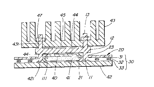
Referring to Fig. 3, an electronic package using the
supporting member 10 includes an LSI chip 40 of size typically
of 17.5 mm x 17.5 mm. An integrated circuit is formed on the
lower surface of the LSI 40. The LSI chip 40 has about 800
input/output terminals (not shown) on the lower surface
thereof . The terminals are aligned with about an 80 ~,m pitch.
The terminals of the LSI chip 40 are connected to the inner
leads 21 of the tape carrier 20. The LSI chip 40 is received
into the device hole 24 of the tape carrier 20. The lower
surface of the LSI chip 40 and the inner leads 21 of the tape
carrier 20 are encapsulated in a resin layer 41.
The bottom legs 11 of the supporting member 10 are inserted
into the holes 23 of the tape carrier 20. The upper surface of
the LSI chip 40 is attached (e.g., glued) to the lower face of
the plate 12 of the supporting member 10 by an adhesive 44. The
adhesive 44 is preferably an epoxy-type adhesive including
silver powder as a filler. Au/Sn-type solders can be used as
the adhesive 44 instead of resin. When the LSI chip 40 is
attached by a solder, a layer of Ti/Au or Ni is formed on the
upper surface of the LSI chip 40 and the lower face of the plate
12.
The bottom legs 11 are connected (e. g., soldered by solder
111) to pads 421 on a substrate 42. Any type of substrate can
be used as the substrate 42. Among the substrates used as the
-11-
CA 02147396 1999-OS-07
substrate 42 are typically glass epoxy substrates, polyimide
substrates, and ceramic substrates.
Pads 33 are formed on the upper face of the substrate 42.
The pads 33 are connected to the pads 31 of the tape carrier 20
via solder bumps 32. The pads 31, the solder bumps 32, and the
pads 33 form a connecting structure 30.
A heat sink 43 is attached to the upper face of the plate
12 of the supporting member 10. The upper legs 13 of the
supporting member 10 are inserted into holes 431 bored in the
heat sink 43. The threaded upper portions of the upper legs 13
protrude through the upper face of the heat sink 43. Suitable
fasteners (e.g., nuts) 47 are screwed onto the upper portion of
the upper legs 13 to secure the heat sink 43 to the supporting
member 10. A silicone-type adhesive 45 is provided between the
lower face of the heat sink 43 and the upper face of the plate
12 of the supporting member 10.
The gap between the upper surface of the LSI chip 40 and
the lower surface of the resin layer 41 is about 0.75 mm.
Specifically, the thicknesses of the LSI chip 40 and the resin
layer 41 are approximately 0.45 mm and 0.3 mm, respectively.
The resin layer 41 is kept from contacting the substrate 42.
Thus, the LSI chip 40 is not pressed against the substrate 42
by the weight of the heat sink 43, and the weight of the heat
sink 43 does not produce stress in the tape carrier 20.
Further, the tape carrier 20 is not loosened or pulled off from
the substrate 42 by the heat sink 43 when the substrate 42 is
in an upright position.
Next is described the assembling process of the electronic
package of the first embodiment.
-12-
CA 02147396 1999-OS-07
Referring to Fig. 4(a), in step 1, the terminals of the
LSI chip 40 are connected to the inner leads 21 of the tape
carrier 20. Thereafter, the lower surface of the LSI chip 40
and the inner leads 21 are encapsulated in the resin layer 41.
Referring to Fig. 4(b), in step 2, the adhesive 44 is
uniformly distributed between the upper surface of the LSI chip
40 and the lower face of the plate 12. Thereafter, the LSI chip
40 is attached to the lower face of the plate 12 of the
supporting member 10, and the bottom legs 11 of the supporting
member 10 are inserted into the holes 23 of the tape carrier 20.
Referring to Fig. 4 (c) , in step 3, the supporting member is
positioned such that the bottom legs 11 are placed on the pads
421. Position of the supporting member 10 also positions each
of the pads 31 above the corresponding ones of the pads 33.
The solder bumps 32 are preformed on the pads 33 of the
substrate 42. The solder 111 is pre-applied on the pads 421 of
the substrate 42. After the positioning of the supporting
member 10, the solder bumps 32 and the solder 111 are heated to
connect between the pads 31 and pads 33, which in turn connect
the bottom legs 11 and the pads 421, respectively.
Referring to Fig. 4(d), in step 4, the adhesive 45 is
uniformly distributed between the upper face of the plate 12 and
the lower face of the heat sink 43. Thereafter, the heat sink
43 is positioned on the plate 12. The upper legs 13 of the
supporting member 10 are inserted into the holes 431
(unreferenced in Fig. 4(d)) of the heat sink 43. The nuts 47
press the heat sink 43 against the plate 12 to secure the heat
sink 43 on the plate 12. The heat sink 43 squeezes the adhesive
45 to uniformly distribute and make the adhesive 45 thinner.
-13-
CA 02147396 1999-OS-07
The adhesion of the adhesive 45 takes about 24 hours at room
temperature or about 15 minutes at a temperature of 150°C.
In the aforementioned assembling process, positioning of
the tape carrier 20 as in the conventional processes is
unnecessary because the positioning of the supporting member 10
simultaneously and precisely positions the tape carrier 20 into
a predetermined position.
Further, the aforementioned assembling process does not
include a step for squeezing the adhesive 45 because the nuts
47 press the heat sink 43 against the plate 12, thereby
squeezing the adhesive 45.
Next is described a second embodiment of the present
invention. The second embodiment has several features. A first
feature is forming the bottom legs 11 and upper legs 13 of the
supporting member 10 by inserting pins into the plate 12.
Another feature is adopting a novel connecting structure for the
connection between the tape carrier 20 and the substrate 42.
Referring to Fig. 5, a supporting member 10 of the second
embodiment includes four pins 14. The pins 14 are shaped as
cylindrical columns whose diameter is approximately 1.0 mm. The
pins 14 are preferably made of brass or Kovar, and are
preferably plated with nickel. The lower ends of the pins 14
are connected (e . g. , soldered by the solder 143 ) to the pads 421
on the substrate 42. The solder 143 is preferably Sn 63 wt% -
Pb 37 wto eutectic solder. The pins 14 are threaded to receive
nuts 142.
The LSI 40 is connected to the inner leads 21 of the tape
carrier 20'. The pins 14 are inserted into the holes 23 of the
tape carrier 20'. The tape carrier 20' is connected to the
-14-
CA 02147396 1999-OS-07
substrate 42 via a connecting structure 34. The detailed
structures of the tape carrier 20' and the connecting structure
34 are described in Fig. 6 subsequently.
The size of the plate 12 is predetermined, so that the
plate 12 does not cover the connecting structure 34. In the
second embodiment, the plate 12 is preferably a square whose
sides and thickness are approximately 22 mm and 1-2 mm,
respectively. The plate 12 has through-holes 124 at each
corner. The pins 14 are inserted into the holes 124. The plate
12 is supported by the nuts 142. The LSI chip 40 is attached
(e.g., glued) to the lower face of the plate 12.
The heat sink 43 is attached (e. g., glued) to the upper
face of the plate 12. The upper portions of the pins 14 are
inserted into the holes 431 of the heat sink 43. The heat sink
43 is secured by the nuts 141. The plate 12 and the heat sink
43 are securely held between the nuts 142 and the nuts 141.
The material of the plate 12 is the same as that of the
first embodiment.
Next is described the structure of the tape carrier 20' and
the connecting structure 34.
In the second embodiment, the diameter of the holes 23 of
the tape carrier 20' is set to be approximately 1.1 mm to match
the pins 14. The material of the film 26 and the size of the
device hole 24 are the same as those of the first embodiment.
Referring to Fig. 6, the inner leads 21 and the wirings 22
are formed on the upper surface of the tape carrier 20'. One
end of each of the wirings 22 is connected to one of the inner
leads 21, whereas the other end of each of the wirings 22 is
connected to one of the pads 31'.
-15-
CA 02147396 1999-OS-07
The wirings are preferably made of copper, plated with
gold. The width and the thickness of the wirings are
approximately 40~m and 10-25~m, respectively. The pads 31' are
disposed in a grid pattern with apprximately 1.27 mm pitch. The
detailed structure of the pads 31' is described below.
Referring to Figs. 7(a) and 7(b), each of the pads 31'
includes annular conductor patterns 36 and 39 on the upper and
lower surface of the tape carrier 20', respectively. The outer
diameters of the conductor patterns 36 and 39 are approximagely
250~.m and 600~.m, respectively. The wirings 22 are connected to
the conductor pattern 36.
Referring to Fig. 8(b), each of the pads 31' further
includes a through-hole 38 which is formed in the film 26. The
diameter of the through-hole 38 is set to approximately 150~.m
and 300~,m at the upper and lower surfaces of the film 26,
respectively, thereby tapering the through-hole 38. The
advantages of such a tapered through-hole 38 are described
below. Another conductor pattern 37 is formed on the inner
surface of the through-hole 38. The conductor pattern 37
connects the conductor patterns 36 and 39.
The conductor patterns 36, 37, and 39 are preferably made
of copper plated with gold. The thickness of the conductor
patterns is approximately 20 ~.m.
Next is described the process for connecting the pads 31'
of the tape carrier 20' and the pads 33 of the substrate 42.
Referring to Fig. 8(a), in step 1, solder 35 is applied
onto the pads 33 of the substrate 42. The solder 35 is
preferably Sn 63 wt% - Pb 37 wt% eutectic solder. The height
-16-
CA 02147396 1999-OS-07
and the volume of the solder 35 are approximately 300~.m and
0.6 x 10 lOm3, respectively.
Referring to Fig. 8(b), in step 2, the pad 31' of the tape
carrier 20' is positioned above the solder 35 on pad 33, of the
substrate 42.
Referring to Fig. 8(c), in step 3, the solder 35 is heated
to approximately 200°C - 250°C. By heating, the solder 35 melts
to travel or flow upwardly into the through-hole 38 by
channeling. The solder 35 that thus appears on the upper
surface of the tape carrier 20' and is readily observable.
Next is described how a faulty or failed connection of the
connecting structure 34 is detected. If the solder 35 appears
on the upper surface of the tape carrier 20', the connection is
determined to be completed. However, if the solder 35 is
absent, the connection may be faulty or completely failed.
Thus, the connection failure in the connecting structure 34 can
be detected easily by the absence of solder 35 on the tape
carrier 20'.
Thus, in addition to the features of the first embodiment,
the second embodiment allows an easy detection of a faulty or
failed connection between the tape carrier 20 and the substrate
42.
Next is described a third embodiment of the present
invention. The feature of the third embodiment is a
modification of the means for supporting the plate 12. Other
structures and functions of the third embodiment are the same
or similar to those of the first and second embodiments.
Referring to Fig. 9, in the third embodiment, each of pins
15 have first and second portions. The diameters of the first
-17-
CA 02147396 1999-OS-07
portion 151 and the second portion 152 are approximately 1.0 mm
and 1.6 mm, respectively. The length of the second portion 152
is approximately 1.8 mm. The diameter of the holes 124 of the
plate 12 and the holes 23 of the tape carrier 20' are set to
approximately 1.4 mm and 1.8 mm, respectively. The first
portion 151 can be inserted into the holes 124 of the plate 12,
while the second portion 152 cannot be inserted thereinto. The
plate 12 is supported on the second portions 152 of the pins 15.
The lower ends of the second portions 152 are joined to the
substrate 42 by solder 153. In the third embodiment, the
substrate 42 and solder 153 are preferably a ceramic substrate
and a Au-Sn type solder, respectively. The soldering of the
solder 153 is performed at a temperature of approximately 350°C.
Thus, in addition to the features of the second embodiment,
the third embodiment has several features. One feature is that
the nuts 142 are eliminated. Another feature is that the length
of the gap between the substrate 42 and the plate 12 can be set
precisely.
Next is described the assembling process of the third
embodiment.
Referring to Fig. 10(a), in step 1, the LSI chip 40, which
is connected to the tape carrier 20', is attached to the lower
surface of the plate 12 by the adhesive 44.
Referring to Fig. 10(b), in step 2, the pins 15 are
inserted into the respective holes 23 of the tape carrier 20'
and into the respective holes 124 of the plate 12. The pins 15
are pre-joined to the substrate 42. By inserting the pins 15
into the holes 23, each of the pads 31' is positioned over the
corresponding one of the pads 33.
-18-
CA 02147396 1999-OS-07
Referring to Fig. 10(c), in step 3, the pads 31' and the
pads 33 are joined via solder 35 by the process shown in Figs.
8(a) - 8(c). A good connection is readily detected by the
appearance of the solder 35 at the upper surface of the tape
carrier 20'.
Referring to Fig. 11, in step 4, the heat sink 43 is
secured to the plate 12 by the nuts 141. The adhesive 45 is
provided between the plate 12 and the heat sink 43. By securing
the nuts 141, the adhesive 45 is squeezed to become uniformly
distributed and to have a smaller thickness.
Next is describe a fourth embodiment of the present
invention. A feature of the fourth embodiment is a modification
of the means for joining the bottom legs 11 or pins to the
substrate 42. Other structures and functions of the fourth
embodiment are the same or similar to those of the third
embodiment.
Referring to Fig. 12, pins 16 have first, second, and third
portions 161-163, respectively. The structures of the first and
second portions are the same as those of the third embodiment.
The diameter of the third portions 163 of the pins 16 is
approximately 0.8 mm. The third portion is plated with nickel.
In the fourth embodiment, the substrate 42 is preferably a
glass polyimide-type printed circuit board which is heat
resistant and has a low permittivity. In the substrate 42,
holes 48 are bored having a slightly larger diameter than that
of the third parts 163 of the pins 16. The third portions 163
of the pins 16 are inserted into the holes 48 and joined to the
substrate 42 via solder 164. The solder 164 flows into the gap
between the holes 48 and the pins 16.
-19-
CA 02147396 1999-OS-07
Thus, in addition to the features of the third embodiment,
the fourth embodiment has the following features. One feature
is that the pins 16 are positioned precisely. Another feature
is that the strength of the joint between the pins 16 and the
substrate 42 is enhanced.
Next is described a fifth embodiment of the present
invention. A feature of the fifth embodiment is a modification
of the means for joining the lower legs 11 or pins to the
substrate 42. The other structures and functions are the same
or similar to those of the third and fourth embodiments.
Referring to Fig. 13, in the fifth embodiment, each of the
pins 17 has a first portion 171, a second portion 172, and a
third portion 173 whose diameters are approximately 1.2 mm,
l.6mm, and 0.7 mm, respectively. The length of the second
portion 172 is approximately 0.8 mm. The pins 17 are preferably
made of stainless steel. The third portion 173 is threaded.
In the substrate 42, holes 48 are bored having a diameter
slightly larger than that of the third parts 173 of the pins 17.
The third portions 173 of the pins 17 are inserted into the
holes 48 of the substrate 42. The pins 17 are fixed to the
substrate 42 by tightening nuts 174 threaded on the pins 17.
Thus, in addition to the features of the third and fourth
embodiments, the fifth embodiment has the following features.
One feature is that the pins 16 can be positioned precisely.
Another feature is that the strength of the joint between the
pins 16 and the substrate 42 can be enhanced.
Next is described a sixth embodiment of the present
invention. A feature of the sixth embodiment is a modification
of means for joining the lower legs 11 or pins to the substrate
-20-
CA 02147396 1999-OS-07
42. The other structures and functions are the same or similar
to those of the third and fourth embodiments.
Referring to Fig. 14, in the sixth embodiment, pins 18 have
a first portion 181, a second portion 182, and a press-fitting
spring 183. The configuration of the first portion 181 is the
same as that of the third embodiment.
Referring to Fig. 15(a), the second portion 182 is a plate
whose length is approximately 0.8 mm. The width of the second
portion 182 is greater than the diameter of the holes 48 of the
substrate 42 and the diameter of the holes 124 of the plate 12.
Referring to Fig. 15(b), the spring 183 has a taped end.
Referring to Fig. 15(c), the cross-section of the spring
183 is M-shaped. The spring 183 has resiliency in the direction
indicated by the arrows . When the spring 183 is inserted in the
holes 48 of the substrate 42, the spring 183 tightly fits
(press-fitted) in the holes 48 to fix the pin 18 to the
substrate 42.
Thus, in addition to the features of the third embodiment,
the sixth embodiment has the feature that the pins 18 can easily
be fixed to the substrate 42.
Next is described a seventh embodiment of the present
invention. A feature of the seventh embodiment is that the
plate 12 is made wide to cover the tape carrier 20.
Referring to Fig. 16, in the seventh embodiment, the plate
12 has a first portion 121 and a second portion 122 which cover
the LSI chip 40 and the tape carrier 20, respectively. The LSI
chip 40 is attached to the lower face of the first portion 121
by the adhesive 44. The tape carrier 20 is attached to the
lower face of the second portion 122 by an adhesive 49. The
-21-
CA 02147396 1999-OS-07
material of the adhesive 49 is the same as that of the adhesive
44.
The tape carrier 20 and the substrate 42 are connected via
the connecting structure 30 used in the first embodiment. The
connecting structure 34 used in the second embodiment cannot be
used in the seventh embodiment because the upper surface of the
tape carrier 20 is covered with the second portion 122 of the
plate 12.
Next is described the assembling process of the seventh
embodiment.
Referring to Fig. 17(a), in step 1, the LSI chip 40 is
connected to the inner leads 21 of the tape carrier 20.
Referring to Fig. 17 (b) , in step 2, the lower surface of
the LSI chip 40 is encapsulated by the resin layer 41.
Referring to Fig. 17(c), in step 3, the adhesive 44 is
distributed over the lower face of the first portion 121 of the
plate 12 or over the upper surface of the LSI chip 40. The
adhesive 49 is distributed over the lower face of the second
portion 122 of the plate 12 or over the upper face of the tape
carrier 20. Thereafter, the LSI chip 40 and tape carrier 20 are
attached to the first portion 121 and the second portion 122 of
the plate 12, respectively. The adhesive is cured at a
temperature of approximately 150°C for about 10 minutes.
Referring to Fig. 17 (d) , in step 4, pins 15 are inserted
into the respective holes 23 of the tape carrier 20 and into the
respective holes 124 of the plate 12. Thereafter, the pads 31
and the pads 33 are joined by soldering.
Referring to Fig. 17(e), in step 5, the heat sink 43 is
attached onto the plate 12.
-22-
CA 02147396 1999-OS-07
In the seventh embodiment, the heat sink 43 thermally
contacts the second portion 122 of the plate 12 as well as the
first portion 121. Therefore, the thermal resistance between
the plate 12 and the heat sink 43 is reduced. Furthermore, the
second portion 122 of the plate 12 prevents the tape carrier 20
from warping.
Next is described an eighth embodiment of the present
invention. A feature of the eighth embodiment is boring holes
in the second portion 122 of the plate 12 to adapt the
connecting structure 34 thereto.
Referring to Fig. 18, tape carrier 20 and the substrate 42
are connected by the connecting structure 34 used in the second
embodiment. Holes 123 are bored in the second portion 122 of
the plate 12. Each of the holes 123 is positioned over the
corresponding one of the pads 31' of the connecting structure
34. The holes 123 make the solder 35 visible, which appears at
the upper surface of the tape carrier 20.
Thus, in addition to the features of the seventh
embodiment, the eighth embodiment has the feature that a faulty
or failed connection between the tape carrier 20 and the
substrate 42 can easily be detected by the absence of solder 35.
Next is described modifications of the aforementioned
embodiments of the present invention.
First, the application of the present invention is not
limited to the LSI chip 40. The present invention can be
applied to any type of electronic device.
Secondly, the cross-section of the bottom legs and the pins
can be formed in a variety of shapes. For example, the cross-
-23-
CA 02147396 1999-OS-07
section may be rectangularly-shaped. The holes 23 of the tape
carrier 20 must be shaped to fit the bottom legs and the pins.
Thirdly, the number and configuration of the upper legs,
bottom legs, and pins are not limited to those of the
aforementioned embodiments.
Fourthly, the heat sink 43 may be coated with insulating
material (e. g., epoxy or silicone) to avoid short-circuiting
among the inner leads 21.
Fifth, the present invention can include any type of
cooling means other than the heat sink 43.
The present embodiments are therefore, to be considered in
all respects as illustrative and not restrictive, the scope of
the invention being indicated by the appended claims rather than
by the foregoing description and all changes which come within
the meanings and range of equivalency of the claims are
therefore intended to the embraced therein.
-24-