Note : Les descriptions sont présentées dans la langue officielle dans laquelle elles ont été soumises.
- -- 2148~34
SPECIFICATION
SLIDING CORRELATOR
TECHNICAL FIELD ~
The present invention relates to a sliding `~`
correlator used in a receiver portion of a radio - ;~
device of a CDMA system performing multiple access
using a spectrum spread technique in mobile
communications, which sliding correlator is provided
to establish initial synchronization for despreading a
spread spectrum received signal into a narrow band
signal.
BACKGROUND ART ~
'. ' ' ":
CDMA systems can be roughly divided into a direct
sequence (DS) system and a frequency hopping (FH)
system. In the FH system, each symbol must be
resolved into small elements called chips, and the ~ -
central frequencies of the chips must be varied at a
high rate to generate a signal. This makes it J,',~
difficult to implement the FH system, and hence, the
25 DS system is generally used. In contrast with ~ -
SCPC/FDMA (Single Channel Per Carrier/Frequency
Division Multiple Access) radio devices or TDMA (Time
~;'',
8~4
Division Multiple Access) radio devices, spread
spectrum (SS) radio devices carry out, at a
transmitter side, a common modulation followed by a
secondary modulation using a spreading code sequence,
and transmits a thus bandwidth spread signal. At a
receiver side, on the other hand, the wideband
received signal is despread to restore the original
narrow band signal, followed by the conventional
demodulation. During this despreading process at the
receiver slde, the spreading code sequence in the
received signal must be synchronized with a replica of
the spreading code sequence generated at the receiver
side.
This synchronization of the replica of the
spreading code sequence at the receiver side using the
spreading code sequence in the received signal is
separated into two distinct phases called an initial
acquisition phase and a tracking phase. Since the
autocorrelation of the spreading code sequence can
only be obtained in a range of + one chip, the inltial
acquisition phase must capture the phase difference
between the spreading code sequence and the reference
replica thereof within a range of a small fraction of
the chip interval +Tc. Then, the tracking phase holds
~he code sequences in this range. The present
invention particularly relates to the initial
synchronization, and hence, a conventional initial
21~8~9~
, ~
synchronization method will be described below.
The initial synchronization of the spreading code
sequence is roughly divided into coherent and
incoherent ones. In the coherent synchronization, the
phase of the carrier of a received signal must be
known in advance. Generally speaking, it is difficult ~ ;~
to obtain the phase of the carrier before despreading
because the carrier at the recelving end is not
synchronized with the carrier at the transmitter end.
lO Accordingly, the incoherent synchronization is ,
conventionally used, in which the received signal is ;~
despread by a replica of the spreading code sequence ;~
at the receiving end, followed by a detection using a
square amplitude detection after band limiting, and ~
15 then by a threshold detection. :
, . - .,
The incoherent initial synchronization of a common ,;i
spreading code sequence is performed by multiplying :
the spreading code sequence of a received signal and a
replica of the spreading code sequence at the
~, , "
receiving end, thereby taking correlation between the
two code sequences. Then, the correlation output is
detected, and the establishment of the synchronization
is detected by testing whether or not the detection
output exceeds a threshold. If the synchronization
25 has not yet been established, the phase of the replica ~
of the spreading code sequence is shifted, and the :
detection of the synchronization is tested again.
~;
- 3 ~
,
2148594
This is performed until the synchronization is
established. This method is called sliding
correlation.
The initial synchronization using the sliding
correlation is divided into classes depending on
whether the time interval (dwell time) Id for
integrating a correlation signal is fixed or variable.
The fixed integral time method can be further divided
into a single dwell type and a multiple dwell type.
These types correspond to whether the detection of the
output signal from a detector is achieved by a single
time integral, or by a plurality of time integrals. An
increasing dwell time is required to improve accuracy
of detection of the initial synchronization.
First, the initial synchronization using the
single dwell type sliding correlation will be
explained.
Fig. l shows a block diagram of a conventional
single dwell synchronization system using the sliding
correlation. In an incoherent detection, the
despreading process is not provided with information
about the phase of a carrier. A received signal from
an input terminal 11, which includes noise components,
is multiplied, by means of a multiplier 13, with the
replica of the spreading code sequence fed from a
spreading code sequence replica generator 12, and
thus, the correlation is calculated. The output of
::
5 5~
2~859~ ~
,
the multiplier 13 is passed through a bandpass filter
14, and is amplitude-detected by a square amplitude
detector (square-law detector) 15. The detected
output is integrated by an integral-dump circuit 16 ~ "
over a dwell time Id- The integrated output undergoes
threshold detection by a threshold detector 17, and if
the integrated output is lower than a threshold, a
voltage controlled clock generator 18 is controlled. ;
Thus, the operation rate of the replica generator 12
is controlled by the clock from the voltage controlled
clock generator 18. --
Fig. 2 shows a block diagram of an equivalent
representation of a lowpass single dwell
synchronization system using the sliding correlation.
A received input signal undergoes quadrature detection
to produce an I channel signal and a Q channel signal.
The I and Q channel signals are passed through lowpass
filters 22 and 23, and then converted into digital
signals by A/D converters 24 and 25, respectively.
Although the quadrature-detected outputs subjected to
direct modulation by the spreading code sequence, the
phase of the spreading code sequence is unknown. The
quadrature-detected outputs are supplied to
multipliers 13I and 13Q, and are multiplied by the
replica fed from the spreading code sequence replica
generator 12. The despread I and Q channel signals
are passed through lowpass filters 26 and 27, and are
- 21~85~
square-amplitude-detected by square amplitude
detectors 15I and 15Q. The amplitude-detected signals
are amplitude-combined by an adder 28, integrated by
the integral-dump circuit 16, and are compared with
the threshold by the threshold detector 17.
Fig. 3 shows a block diagram of a multiple dwell
synchronization system. A received signal from the
input terminal 11 is multiplied, by means of the
multiplier 13, with the replica of the spreading code
sequence fed from the spreading code sequence replica
generator 12. The output of the multiplier 13 is
amplitude-detected by the square amplitude detector
15, and the output thereof is inputted to N integral-
dump circuits 161 - 16N. Denoting the dwell times of
the integral-dump circuits 161 - 16N by Id1 ~ ~dN,
respectively, it is assumed that the relationships of
the dwell times of the N integral-dump circuits 161 -
16N are as follows:
Idl < ~d2 < ~d3 ~ -- <~dN
The probability that each output signal Zi exceeds its
; threshold depends on the probabilities that previous
; respective outputs Zk(k: 1, i-1) exceed their own ~
thresholds. In view of this, only when all the levels ~ ;
of the output signals of the previous integral-dump
circuits 161 - 16i_1 exceed their thresholds, the i-th
integral-dump circuit 16i compares its output signal ~-~
with its threshold. If the output of at least one of ~
~ -.. ~ . .
,.. ;~
'"~""
~'','','''.,,,'`.'.,'`.'',"'.,',''','f.'.'~'''' '"` ' '''''"'' ' ' `'' ' ' "': '
~ - 21~8~9~ ; ~
the previous integral-dump circuit 16k is below its
threshold, the phase of the replica of the spreading ,~
code sequence is renewed, and all the integral-dump
circuits l6 are reset to proceed to the next search.
To complete the search for detecting
synchronization, it is necessary to start the test
from the first integral-dump circuit 161, and to -~
continue it sequentially until the test of the output
of the N-th integral-dump circuit 16N has been
completed.
In a word, a synchronization detector (coherent
detector) 32 detects the synchronization in accordance
with the following algorithm.
(1) It judges that the synchronization is ;
established and completes the search when it detects
that all the output signals Zl - ZN of the N integral-
dump circuits 161 - 16N exceed their own thresholds.
(2) If it detects that one of the detector
outputs Zi fails to pass the threshold test, and
20 hence, judges that the current phase state is -
incorrect, it continues the search. In this case, it
delays by a predetermined amount the phase of the
replica of the spreading code sequence produced from
the spreading code sequence replica generator 12~. ~
In the multiple dwell synchronization system with ;
the arrangement of Fig. 3, the maximum time for
detecting whether the synchronization is established
~ .
2148~94
. .
or not about the spreading code sequence or a
particular phase is IdN~ and the minimum time is ~dl-
Accordingly, the synchronization can be detected for
almost all the phases of the replica of the spreading
code sequence in a test interval of the dwell time Idk
(k < N). In the single dwell synchronization system,
on the other hand, the test interval equals ~dN in all
the cells. Thus, the multiple dwell synchronization
system can shorten the initial synchronization time as
compared with the single dwell synchronization system.
In the multiple dwell synchronization system, the
integral time interval of respective integral-dump
circuits 161 - 16N overlap with each other.
Accordingly, an actua~ circuit can be implemented by a
single integrator without using the N parallel
integral-dump circuits 161 - 16N. The single
` integrator outputs intermediate values at the times t
= ~dl, ~d2, -- IdN~ and the outputted integrated
values are sequentially compared with their
thresholds. The integrator is reset when the
:., -
~ synchronization is not detected, and hence, the search ~ ~
., ~
of the next phase of the spreading code sequence must
be started. ~ `
Since the sliding correlators obtain the
correlation between the spreading code sequence in the
received signal and the replica of the spreading code -
sequence which is generated at the receiving end, by
' ~" ''.~; .
21485~'1
time integrations, they can be arranged as a
considerably small circuit appropriate to be :
constructed into an LSI circuit. The sliding
correlator, however, takes a long time to establish
5 the initial synchronization because of time .
integrations as described above. - .
It is therefore an object of the present invention ~:-
to provide a sliding correlator that can establish .
synchronization quickly. . :
: ; '
DISCLOSURE OF THE INVENTION
In a first aspect of the present invention, there :
is provided a sliding correlator comprising: : .
a memory circuit for storing a received signal;
a timing generator for generating a clock signal .;
` used for reading the received signal stored in the ~-.
: memory circuit at a frequency substantially higher - :
than a storing rate of the receive signal;
a spreading code sequence replica generator for
generating a replica of a spreading code sequence;
a multiplier for multiplying the read received
signal with the replica of the spreading code
sequence;
an accumulator for accumulating an output signal ~
of the multiplier over a predetermined time period; : ~;
a threshold detector for detecting whether or not :
21~859~
an output signal of the accumulator exceeds a
predetermined threshold; and
a clock generator for controlling the spreading
code sequence replica generator to generate the
spreading code sequence at the same rate as that of
the clock signal, the clock generator changing a phase
of the replica of the spreading code sequence when a
detection output of the threshold detector is less
than the threshold.
In a second aspect of the present invention, there ~:
is provided a sliding correlator comprising:
a memory circuit for storing a received signal;
a timing generator for generating a clock signal ~ :
used for reading the received signal stored in the;:
memory circuit at a frequency substantially higher
than a storing rate of the receive signal; ;.~;.
a spreading code sequence replica generator for -:-:
generating a plurality of replicas of a spreading code
sequence, the replicas having different phases;
a plurality of multipliers, each of which :
multiplies the read received signal by one of the
: plurality of replicas of the spreading code sequence;
a plurality of accumulators, each of which .~.
accumulates an output signal of one of the plurality ~-~
25 of multipliers over a predetermined time period; : .
a threshold detector for detecting whether or not
each of output signals of the plurality of ;
- 1 0 - ' '" '`'""" '' ''
,, , ~, I;
21485~4
-
~
accumulators exceeds a predetermined threshold; and
a clock generator for controlling the spreadingcode sequence replica generator to generate the
spreading code sequence at the same rate as that of
the clock signal, the clock generator changing a
phases of the replicas of the spreading code sequence
by using an output of the threshold detector when all
output signals of the plurality of the accumulators
are less than the threshold.
The sliding correlator in accordance with the
present invention can be applied, for example, to a
receiver of a CDMA system which performs multiple
access by using spread spectrum in a mobile
communication system, and can quickly establish the
initial synchronization for despreading a received
signal into a narrow band signal.
~ :.
BRIEF DESCRIPTION OF THE DRAWINGS
Fig. l is a block diagram showing a conventional
single dwell synchronization system;
Fig. 2 is a block diagram showing a conventional
quadrature detection sliding correlator;
Fig. 3 is a block diagram showing a conventional
multiple dwell synchronization system;
Fig. 4 is a block diagram showing an embodiment of
a sliding correlator in accordance with the present
5 9 ~ :
invention;
Fig. 5 is a dlagram illustrating the operation of
the sliding correlator shown in Fig. 4i
Fig. 6 is a block diagram showing another
embodiment of a sliding correlator in accordance with
the present invention; and
Fig. 7 is a diagram illustrating the operation of
the sliding correlator shown in Fig. 6.
BEST MODE FOR CARRYING OUT THE INVENTION
Embodiments of the present invention will now be
described with reference to the accompanying drawings.
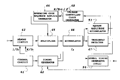
Fig. 4 is a block diagram of a basic embodiment of
a sliding correlator in accordance with the present
invention. ln Fig. 4, the reference numeral 43
designates a memory circuit for storing A/D converted
received signal corresponding to a dwell time ~d plus a ;~
predetermined amount a. The reference numeral 42
denotes a timing generator which generates, under the
control of a control circuit 41, a write timing signal
and a read timing signal, which are supplied to the
memory circuit 43. The rate of the read timing signal
is K times higher than that of the write~timing
signal. The reference numeral 45 designates a
multiplier which multiplies the received signal read `~
from the memory circuit with a replica of the ~ ~`
- 12 ~
.'`''`~
;, . .
.- ~
~i~8~9~
.
spreading code sequence fed from a spreading code
sequence replica generator 44. The reference numeral
46 denotes an accumulator which accumulates the
product of the replica and the spreading code sequence
of the received signal over the dwell time ~d. The
reference numeral 47 designates a threshold detector
which detects whether or not the initial
synchronization is established on the basis of the
accumulated value of the product of the replica and
the spreading code sequence of the received signal
over the dwell time ~d. The reference numeral 48
designates a voltage controlled clock generator for
generating, in response to the output of the threshold
detector 47, a clock signal to be supplied to the
spreading code sequence replica generator 44. The
output of the threshold detector 47 is also inputted
to the timing generator 42 to control the read timing
signal supplied to the memory circuit. The reference
numeral 53 designates a square amplitude accumulator
which accumulates the received signal multiplied by
the replica of the spreading code sequence over one
symbol interval after the initial synchronization has
been established. The reference numeral 54 denotes a
symbol timing generator composed of a DPLL (Digital
Phase-Locked Loop) which generates the symbol timing
based on the output from the square amplitude
accumulator 53 and the output from the timing ;
- 13 -
~1~859Q
generator 42.
Fig. 5 is a diagram illustrating the operation of
the initial synchronization of the embodiment with the
arrangement as shown in Fig. 4. The sliding
correlation operation of the embodiment for the
initial synchronization will now be described with
reference to Figs. 4 and 5.
In the explanation below, we assume the following:
The dwell time Id is made equal to one symbol interval
in this embodiment because the dwell time is usually
set at that value. The memory circuit 43 has a
capacity capable of storing the received signal
corresponding to 1 symbol + ~. Furthermore, the ;
frequency of the write timing signal and that of the -~
read timing signal produced by the timing generator 42
are set at l/TC and K/TC, respectively, where TC is
one chip period. Accordingly, M correlation values
(multiplications) are obtained by the accumulation, -
where M = one symbol period / TC. These assumptions --`
can be changed rather arbitrarily.
The timing generator 42 begins to output the write
timing signal in response to a start signal from the
control circuit 41, and the A/D converted received
signal is stored into the memory circuit 43 (see, (A)
25 of Fig. 5). When the xeceived signal is stored by an ~ ',','!'.
amount corresponding to the dwell time ~d (that is, an
amount corresponding to one symbol in this case), the
- 19 -
,. , .
2~8~94
.. :
read timing signal whose frequency is K times that of
the write timing signal is outputted from the timing
generator 42. Thus, the received signal is read out
of the memory circuit 43 at a rate K times higher than
the writing rate (see, (B) of Fig. 5). The read
received signal and a replica (see, (C) of Fig. 5) of
the spreading code sequence are multiplied by the
multiplier 45, the replica being generated by the
spreading code sequence replica generator 44 at the
same frequency as the read timing signal, and the
product is accumulated by the accumulator 46 over the
dwell time ~d (one symbol period in this case). The
threshold detector 47, receiving the output of the
accumulator 46, detects whether the initial
synchronization is established.
If the synchronization is not established, the
voltage controlled clock generator 48 controls, in
accordance with the output of the threshold detector
47, the spreading code sequence replica generator 44
so that the phase of the replica of the spreading code
sequence therefrom is delayed by one chip interval.
In addition, the same received signal is read again by
the read timing signal outputted from the timing
generator 42 in response to the output of the
threshold detector 47. Then, the multiplication and
the accumulation are performed again, and the result
is inputted to the threshold detector 47. The above-
- 15 -
~:.'.. , , . , ,, ' . ,, : : '
2148~4
mentioned operation is repeated until the threshold
detector 47 detects that the inltial synchronization
has been established.
When the threshold detector 47 detects that the ~ ;~
initial synchronization is established, its output is
supplied to the timing generator 42 and the voltage
controlled clock generator 48, thereby stopping the
sliding operation for the initial synchronization.
Subsequently, the timing generator 42 and the voltage
controlled clock generator 48 output a timing signal
of the chip period or the like rather than of K times
the normal rates.
Since the present invention performs the
correlation detecting operation at a rate K times
higher than the chip frequency, the interval required
to establish the initial synchronization is reduced by `-`
a factor of K as compared with the conventiona]
sliding correlation, which enables a high speed
synchronization.
The timing signal of symbols of the synchronized
received signal is amplitude-squared by the square
amplitude accumulator 53, and accumulated over one
symbol interval, so that its result is supplied to the
symbol timing generator 54, and the symbol timing is
formed.
It is sufficient for the memory circuit to have a
capacity that can store the received signal
- 16 - ~'~
`:.
~1~83~4
, ~ . ;
corresponding to the dwell time ~d during which the
received signal is read out repeatedly (an amount
corresponding to the received signal during one symbol
lnterval in this case), plus a capacity that can store
the received signal in the worst case for establishing
the initial synchronization.
High speed synchronization establishment is
necessary for the sliding correlator to be applied to
CDMA mobile communications. In particular, in the
control channel establishment before entering
communications, a base station is required to
correctly receive, from the very beginning, a reversal
control channel signal from a mobile station. In this
case, the receive timin~ of the control channel signal
at the base station can be roughly estimated on the
basis of the transmission timing of a control channel
signal from the base station to the mobile station.
The control circuit 41 controls the timing generator
42 so that the writing to the memory circuit 43 is
started at that timing.
Although the sliding correlator of Fig. 4 is a
single dwell type, the present invention can also be
applied to a multiple dwell type. In this case, the
arrangement of Fig. 4 may be modified to include a
plurality of accumulators 46, each provided in order
to accumulate over different dwell times, and the
outputs of the accumulators are inputted to the
: :,. , . -, . . , . . : . - -
:- . ~ .. - . - , : : : .
.,::- . : - , . . , . . ~ . .
~148~94
, . . ..
- ....... , ,:
threshold detector ln parallel so that the detection
is made in terms of each of the inputs.
Alternatively, the accumulator 46 may be constructed
so that it produces intermediate values which are used
for detection. Although it is assumed that the A/D
conversion and the writlng to the memory circuit are
performed at one chlp perlod, lt ls obvious that these
operations can be carried out at a higher rate.
Moreover, the initial synchronization can be
established at a higher rate by performing parallel
calculatlons by replacing the multipller 45 and the
accumulator 96 by a plurality of multipliers and
accumulators in the sliding correlator shown in Fig.
4. An example of this is shown in Fig. 6. ~-
In Fig. 6, the reference numeral 11 designates an
lnput terminal, 21 deslgnates a quadrature detector,
22 and 23 deslgnate lowpass filters, and 24 and 25
designate A/D converters. The reference numeral 43 -
designates a memory circuit, 56 denotes N complex
20 multipliers, 57 designates N accumulators which can -~
perform parallel operation. The reference numeral 58
designates a threshold detector which parallelly
detects thresholds of the accumulated values from the
plurality of accumulators. The reference numeral 51
25 designates a square amplitude detector, 52 denotes a `
loop filter, 48 designates a voltage controlled clock ;~
generator, all of which perform tracking. The voltage ~
,. ': ''
'' ''"' ':
, :. - .
- 18 - ~
:
~'. ', :
'' .
~148~94
controlled clock generator 48 is used to establish the
initial synchronization, as well. The reference
numeral 55 designates a spreading code sequence
repllca generator that can parallelly generate
replicas corresponding to a plurality of phases of a
spreading code sequence. The control circuit 41, the
timing generator 42, the square amplitude accumulator
53, and the symbol timing generator 54 are the same as
those shown in Fig. 4.
The initial synchronization establishing operation
of the parallelly operating sliding correlator as
shown in Fig. 6 will be described with reference to
Fig. 7. In this case, the conditions identical to
those in connection with Figs. 4 and 5 are assumed.
The received signal from the input terminal 11 is
converted into baseband signals through the quadrature
detection by the quadrature detector 21. The baseband
signals are passed through the lowpass filters 22 and -
23, and converted into digital signals by the A/D
converters 24 and 25, which digital signals are
inputted to the memory circuit 93 (see (A) of Fig. 7). ~
The memory circuit 43 performs writing and reading, as -
the memory circuit shown in Fig. 4 does, in accordance
with the write timing signal and the read timing
signal from the timing generator 42 controlled by the
control circuit 41. The rate of the read timing
signal is K times higher than that of the write timing
- 19 -
21~8~94
signal (whose period equals chip period TC in this
example). The same received signal is provided from
the memory circuit 43 to the N complex multipliers 56.
The spreading code sequence replica generating portion
5 55 provides respective multipliers 56 with codes ~;;
having different phases but corresponding to the same ~;
spreading code sequence. The outputs of the
multipliers 56 are each accumulated by the
accumulators 57 individually over the dwell time ~d-
Then, the threshold detecto- 47 detects the
synchronization in terms of individual accumulated
signals. The outputs of the spreading code sequence
generator 55, of the complex multipliers 56, and of
the accumulators 57, and the inputs of the threshold
detector 58 are all parallel, thereby forming N paths.
The respective complex multipliers 56 are provided
in parallel from the memory circuit 43 with the same
received signal which is read out by the read timing
signal whose rate is K times that of chip rate (see,
(B) of Fig. 7). In addition, the N complex
multipliers 56 are provided from the spreading code ~-~
sequence replica generator 55 with replicas having
different phases but corresponding to the same -
spreading code sequence generated at the same
frequency as the read timing signal. For example, the
first complex multiplier is provided from the
spreading code sequence replica generator 55 with a
- 20 -
-- 214859~
replica of the spreading code sequence, which replica
has no phase difference (see, (C-1) of Fig. 7). The
second complex multiplier is provided with a replica
of the spreading code sequence, which replica has a
phase difference of M/N chip (see, (C-2) of Fig. 7).
Finally, the N-th complex multiplier is provided with
a replica of the spreading code sequence, which
replica has a phase difference of (N-l)M/N chip (see,
(C-2) of Fig. 7). The complex multipliers 56 each
perform complex multiplication chip by chip, and the
accumulators 57 accumulate the products, respectively.
Then, the threshold detector 58 detects whether the
initial synchronization is established in terms of
respective accumulations (that is, respective paths)
after the complex multiplications and the
accumulations have been performed over the dwell time
~d-
When the threshold detector 58 detects that noinitial synchronization is established in any of the
paths, it controls with its output the voltage
controlled clock generator 48, thereby shifting the
phases of all the replicas of the spreading code
sequence by one chip, the replicas being generated by
the spreading code sequence generator 55. The output
of the threshold detector 58 is also applied to the
timing generator 42 to restart the reading of the
received signal from the memory circuit 43. The
~148~4
operation is continued until the decision is made that
the initial synchronizatlon is established. Since the
circuit performs the calculation in parallel through N
paths, the time for establishing the initial
synchronization can be reduced by a factor of N in
this circuit.
When the threshold detector 58 detects that the
initial synchronization is established in any one of
the paths, it controls the voltage controlled clock
generator 48, thereby adopting the phase of the path,
in which the synchronization has been established, as
the phase of the repllca of the spreading code
sequence used for despreading from now on. Thus, the ;
sliding operation for the initial synchronization has
15 been completed. After this, the reading of the memory :,
circuit 43 and the generation of the replica of the
spreading code sequence are performed at the chip ~-
interval Tc. -
On completing sliding for establishing the initial
synchronization, a tracking operation is started. The
tracking is carried out by generating a code having a
phase advance of one chip with respect to the replica
of the spreading code sequence with which the initial
synchronization has been established, and a code
having a phase delay of one chip with respect to the
same replica by means of the spreading code sequence
replica generator 55, and then, detecting correlafion
8594
between the two codes. After the initial
synchronlzation has been established, the complex
multipliers 56 multiply the received signal with the
code having the phase advance of one chip with respect
to the replica of the spreading code sequence, and
with the code having the phase delay of one chip,
respectively. The products are accumulated by the
accumulators 57 over one symbol interval so that the
phase difference can be obtained. The two signals
having a phase difference are each amplitude-squared
by the square amplitude detector 51 to remove the
transmission information component, and are added
thereafter. This makes it possible to achieve
tracking using an S curve characteristic. The output
of the square amplitude detec~or 51 is averaged over a
several symbol interval by the loop filter 52, thereby
obtaining a phase error signal. The phase error
signal is then inputted to the voltage controlled
clock generator 48 so that the tracking is carried out
by shifting the replica by one chip in accordance with
the phase error signal.
INDUSTRIAL APPLICABILITY
As described above, the sliding correlator in -
accordance with the present invention is used in the
receiver portion of a CDMA system which performs
21~8~94 :
multiple access by using spread spectrum in mobile
communications, for example, and can establish the ::
initial synchronization quickly for restoring a narrow
band signal by spectrum despreading.
'~'
, ::;
- 24 - .:~