Note : Les descriptions sont présentées dans la langue officielle dans laquelle elles ont été soumises.
I~ a~
~- 21~9837
TITLE OF THE l~V ~:N'llIoN
COMMUNICATION SYSTEM CAPABLE OF PREVENTING DROPOUT OF
DATA BLOCK
BACKGROUND OF THE INVENTION
Field of the Invention
The present invention relates to such a communication
system for transmitting real time data, e.g., video data
and audio data with employment of the communication control
bus such as the serial bus standardized by IEEE-P1394 (will
be simply referred to a "P1394 serial bus" hereinafter).
Description of the Related Art
A communication system is conceivable such that a
plurality of electronic appliances are connected to each
other via the communication control bus such as the P1394
serial bus, and both digital information signals and
control signals are communicated among these electronic
appliances.
In Fig. 3, there is shown an example of such a system.
This system is comprised of electronic appliances A, B, C
connected to each other via the P1394 serial bus. These
electronic appliances are, for instance, a digital VTR, a
tuner, a monitor and the like. The respective electronic
appliances include such a circuit with an essential
Y8~7
function, for example, a recording/reproducing unit for a
digital VTR, as a display unit for a monitor in addition to
a circuit for transmitting/receiving a signal via the P1394
serial bus.
A data transmission is carried out among the
electronic appliances "A" to "C" which commonly share the
P1394 serial bus every a predetermined communication cycle,
as illustrated in Fig. 4. With respect to the management
of the communication cycle, a predetermined electronic
appliance for managing the communication system, for
instance, the electronic appliance A transfers the cycle
start data indicative of the starting time of the
communication cycle via the P1394 bus to other electronic
appliances, so that the data transmission in this
communication cycle is commenced.
The time information on the P1394 serial bus is
managed by a timer register owned by each of these
electronic appliances. The timer registers employed in the
respective electronic appliances count the own clocks to
produce the time information. This time information is
reset on the basis of the timing of the cycle sink every
125 microseconds (see Fig. 4). Then, this time information
is corrected based on the time information given to the
cycle start data.
As a data format transmitted within 1 communication
`~ 21~9837
cycle, there are two sorts of data format, i.e., a
synchronous type data packet such as video data and audio
data, and an asynchronous type data packet such as a
connection control command. Then, the synchronous type
data packet is transmitted prior to the asynchronous type
data packet. Fig. 4 represents only the synchrounos type
data packet.
In the communication system with such an arrangement,
when the communication cycle is repeated every 125
microseconds under ideal condition, the time period at
which the timer registers employed in the respective
electronic appliances are reset is coincident with that of
the cycle start data. However, when the transmission time
of the asynchronous type data packet is prolonged, since
the timing at which the next communication cycle is
commenced is delayed, the timing of the cycle start data is
delayed, as compared with that of the cycle sink.
Considering such a case that in the above-described
communication system, both of the video data and the audio
data (will be referred to "AV data" hereinafter), which are
outputted by the digital VTR, are transmitted to another
video VTR.
Fig. 5 represents a model such that the AV data is
packeted to be transmitted. The AV data reproduced by the
digital VTR are arranged as an array of data blocks having
` 214~837
constant sizes, as shown in Fig. 5(a), and then arrive at
the transmitter circuit. This data block process is
performed by using the FIFO employed between the
recording/reproducing unit of the digital VTR and the
transmitter circuit. The data blocks arrived to this
transmitter ci`rcuit are numbered in the serial data block
number, and are packeted in the unit of data block, and
then the packeted data blocks are sent out to the data bus.
At this time, the data blocks which have reached during a
time period from one preceding cycle sink to the present
cycle sink are packeted in accordance with the data block
numbers from the lower numbers to the higher number, and
then the packeted data blocks are transmitted after the
cycle start data.
In Fig. 5, since the data blocks arrive to the
transmitter circuit in an interval of approximately 50
microseconds, when the normal communication is carried out,
the number of data blocks transmitted by one packet is
eq~al to either 2 or 3.
Furthermore, referring now to Fig. 8, another concrete
example of such a communication system will be explain.
This communication system is equipped with a TV, a VTR 1, a
VTR 2, and a camcoder (will be referred to a "CAM"
hereinafter) as the AV appliance. Then, the P1394 serial
buses capable of transmitting the digital AV signal and the
`~ 21~837
control signal in the mixture state are employed to connect
the CAM with the TV, the TV with the VTR 1, and the VTR 1
with the VTR 2. Each of these appliances owns the function
to relay the control signal and the digital AV signal on
the P1394 serial bus.
Fig. 9 is a block diagram for indicating a basic
arrangement of a VTR corresponding to one example of the AV
electronic appliance employed in the communication system
of Fig. 8. This VTR includes as the basic blocks of the
VTR, a deck unit 1, a tuner unit 2, an operation unit 3
functioning as a user interface, a display unit 4, and a
microcomputer 5 for controlling the overall operations of
the VTR, for producing a packet (will be described later),
and for holding an address. This VTR further comprises a
digital interface (will be referred to a "digital I/F"
hereinafter) 6 for the P1394 serial bus, and a switch box
unit 7 for switching signals among the deck unit 2, the
tuner unit 2, and the digital I/F 6.
It should be noted that when a TV is employed as the
AV appliance, a monitor unit and an amplifier unit are used
instead of the deck unit 1, and no display unit 4 is
employed. In case of CAM, a camera unit is provided
instead of the tuner unit 2.
As illustrated in Fig. 10, a data transmission is
performed in a preselected communication cycle (for
~`` 21~9837
example, 125 microseconds) in the communication system of
Fig. 8. Then, both of the synchronous communication and
the asynchronous communication can be carried out. In the
synchronous communication, the data signal such as the
digital AV signal is continuously transmitted at a constant
data rate, whereas in the asynchronous communication, the
control signal such as the connection control command is
irregularly transmitted, if required.
The cycle start packet CSP is present at the beginning
of the communication cycle, and subsequently, a time period
is set during which the packet for the synchronous
communication is transmitted. The channel numbers 1, 2, 3,
---, N are attached to the respective packets for
performing the synchronous communication, so that a
plurality of synchronous communications can be achieved.
Assuming now that the channel 1 is allocated to the
communication performed from the CAM to the VTR 1, the CAM
transmits the synchronous communication packet attached
with the channel number 1 is transmitted just after the
cycle start packet CSP, the data bus is monitored by the
VTR 1, and then the synchronous communication packet
attached with the channel number 1 is acquired to perform
the communication. Furthermore, when the channel 2 is
allocated to the communication from the VTR 2 to the TV,
both of the communication from the CAM to the VTR 1 and the
`-_ ` 2149837
communication from the VTR 2 to the TV can be carried out
in a parallel manner.
Then, after the transmission of the synchronous
communication packets for all of the channels have been
completed, the time period up to the next cycle start
packet CSP is used as the asynchronous communication. In
Fig. 10, packets A and B correspond to the asynchronous
communication packets.
In the communication system with employment of the
P1394 serial bus, when the respective AV electronic
appliances are connected to each other via the serial
buses, the node ID (physical address) is automatically
allocated in accordance with this connection conditions.
In case of Fig. 8, symbols #0 to #3 correspond to the node
ID. Next, the allocating sequence of the node ID will be
simply explained with reference to Fig. 11.
In Fig. 11, such a hierarchical structure is made that
a leaf node B and a branch node C are connected to the
lower grade of the route node A, and further a leaf node D
and a leaf node E are connected to the lower grade of the
branch node C. In other words, the node A corresponds to
the parent node for the nodes B and C, and the node C
corresponds to the parent node for the nodes D and the node
E. First, a description will be made of the sequence for
determi n ing this hierarchical structure.
,`" 2149837
When a twist-pair cable of the P1394 serial bus is
used to connect the nods A and B, the nodes A and C, the
nodes C and E, the node in which only one input/output port
is connected to another node transfers such a message to
the node connected with the own node that the counter node
corresponds to the parent node.
In case of Fig. 11, the node B transfers such a
message that this node B corresponds to the parent node for
port 1 of the node A, the node D transfers such a message
that this node D corresponds to the parent node for the
port 2 of the node C, and the node E transfers such a
message that this node corresponds to the port 3 of the
node C.
As a result, when the node A recognizes that the child
node is connected to the port 1, the port 1 notifies tot he
node B that it corresponds to the child node. Also, the
node C notifies from the port 2 thereof to the node D that
it corresponds to the child node, and notifies from the
port 3 thereof to the node E that it corresponds to the
chile node.
Then, such nodes that a plurality of input/output
ports are connected to other nodes transfer messages that
the counter nodes correspond to the parent node, with
respect to nodes other than the nodes to which such a
message has been transferred that they are the parent
2149~37
nodes.
In case of Fig. 11, the node C notifies to the port 2
such a message that the node A corresponds to the parent
node, and the node A notifies to the port 1 of the node C
such a message that the node C corresponds to the parent
node. At this time, since the counter nodes will notify
between the node A and the node C such messages that they
correspond to the parent nodes, the node which has first
received such a messagé that this node corresponds to the
parent node becomes the parent node.
If the counter nodes transfer at the same time such
messages that they are the parent nodes, then after the
nodes are brought into the waiting time set at random by
the respective nodes, the counter nodes notify that they
are the parent nodes. Fig. 11 indicates such a case that
the node A becomes the parent node.
It should be noted that in the above description, the
nodes B, D, E whose single input/output port is connected
to other node transfer such a message that the counter node
corresponds to the parent node with respect to the node
connected to the own node. Alternatively, for instance,
when the timing of the node B to transfer the message that
the node A corresponds to the parent node is delayed, and
the node B has transferred in advance the message that the
node A corresponds to the parent, the node B becomes the
~ 21~98~7
route node.
Subsequently, a description will now be made of the
sequence to apply the physical addresses to the respective
nodes. Basically, a physical address of a node is applied
in such a manner that a parent node allows to apply a
physical address to a child node. When there are plural
child nodes, for example, the parent node will allow to the
physical addresses to such child nods which are connected
to the lower (younger) port numbers.
In Fig. 11, when the node B is connected to the port 1
of the node A and the node C is connected to the port 2,
the node A allows to give the physical address to the node
B. The node B transmits to the bus the data for indicating
that the node ED#O is applied to the own node and the node
ID#O has been applied to the own node.
Next, the node A allows to determine the address with
respect to the node C. The node C allows to apply the
address to the node D connected to the port 1. The node D
applies the node ID#l to the own node.
Subsequently, the node C allows to apply the physical
address to the node E connected to the port 2. The node E
applies the node ID#2 to the own node E. When the node C
has completed the address applications to the child nodes D
and E, the node C applies the node ED#4 to the own node.
It should be noted that a detailed description about
21498~7
thé P1394 serial bus involving the sequence to allocate
this node ID is disclosed as "IEEE P1394 Serial Bus
Specification" (issued on October 14, 1993).
There are four prior patent applications:
1). EPC Laid-open No. 0614297,
2). Japanese Patent Application No. 5126682,
3). Japanese Patent Application No. 5200055,
4). Japanese Patent Application No. 6051246,
and the corresponding US patent applications are still
pending.
When the AV data is transmitted in such a way, as
shown in Fig. 6, if the cycle start data is dropped out due
to noise appearing on the bus and the bus reset operation,
then the data blocks 2 and 3 would be dropped out which
should be originally transmitted in the communication cycle
commenced from this cycle start data. This is because the
protocol for the P1394 serial bus determines that after the
cycle start data has been detected, the data block is
transmitted.
Accordingly, as illustrated in Fig. 7, in order that
the data blocks are not dropped even when the cycle start
data is dropped out, the data blocks 2 and 3 which should
be originally transmitted in the communication cycle
starting with the dropped cycle start data may be
transmitted in the communication cycle commenced from the
11
_`` 2149837
next normal cycle start data. However since total number
of data blocks transmitted as a single data packet is
increased to 5, the operation frequency band (bus
occupation time) would also be increased. If more than two
cycle start data would be continuously dropped out, then a
total number of data blocks transmitted as a single data
packet will be further increased, namely the operation
frequency band will be further increased. As a result,
there is such a problem that the frequency band could not
be effectively utilized.
The present invention has been made to solve such a
problem, and therefore has an object to provide a
communication system capable of effectively using a
frequency band. Also, the present invention has another
object to provide a communication system capable of
preventing a dropout of a data block, and further capable
of effectively using a frequency band.
SUMMARY OF THE INVENTION
To solve the above-described problems, according to
the present invention, in a communication system for
transmitting more than one data block arrived for every
preselected time period as a packet subsequent to a
communication start signal at a time period next to the
time period when said more than more data ~lock has
12
21~98~7
arrived, a m~ximum number of data blocks capable of being
transmitting within a predetermined time period is
determined.
The communication system of the present invention is
arranged by that:
when a communication start signal is dropped out, such
data blocks lower than the m~ ximum data block number are
transmitted by way of a packet subsequent to a normal
communication start signal, among data blocks which have
arrived within a time duration defined from a starting time
instant of a preselected time period during which the
normal communication start signal is obtained after said
communication start signal was dropped out up to a
preselected time.
Furthermore, the predetermined time is equal to two
times longer than the predetermined time period. Then, the
communication system of the present invention is arranged
by that:
when the number of data blocks which have arrived
within a time duration defined from a starting time instant
of a period where a normal communication signal is obtained
after the communications tart signal is dropped out up to a
predetermined time, exceeds the m~Ximum value of the data
blocks transmittable within one preselected time period,
the data block having the m~ximum data block number is
13
21~9837
transmitted from the previously arrived data blocks.
In accordance with the present invention, the data
blocks whose number is lower than the m~ximum data block
number are transmitted as the data packet within a single
preselected time period. As a consequence, since the
operation frequency band does not exceed the m~ ximum data
block number, other data are transmitted via the remaining
frequency band, so that the operation frequency band can be
effectively used.
Also, according to the present invention, when a
communication start signal is dropped out, such data blocks
lower than the mAxi mum data block number are transmitted by
way of a packet subsequent to a normal communication start
signal, among data blocks which have arrived within a time
duration defined from a starting time instant of a
preselected time period during which the normal
communication start signal is obtained after the
communication start signal was dropped out up to a
preselected time. Accordingly, even when the communication
start signal is dropped out, it is possible to prevent the
data block from being dropped out, and also the frequency
band can be effectively utilized.
Then, according to the present invention, when the
number of data blocks which have arrived within a time
duration defined from a starting time instant of a period
14
21~983~
where a normal communication signal is obtained after the
communication start signal is dropped out up to a
predetermined time, exceeds the m~xi mum value of the data
blocks transmittable within one preselected time period,
the data block having the m~x; mum data block number is
transmitted from the previously arrived data blocks.
As previously described in detail, according to the
present invention, since the m~ximum number of data blocks
capable of being transmitted as a data packet within one
predetermined time period is determined, the operation
frequency band can be effectively utilized.
Also, according to the present invention, since when
the communication start signal is dropped out, such data
blocks lower than the m~ximum data block number are
transmitted by way of the packet subsequent to the normal
communication start signal, among data blocks which have
arrived within the time duration defined from the starting
time instant of a preselected time period during which the
normal communication start signal is obtained after the
communication start signal was dropped out up to a
preselected time, it is possible to prevent the data blocks
from being dropped out, and to effectively use the
operation frequency band.
BRIEF DESCRIPTION OF THE DRAWINGS
2149837
For a better understanding of the present invention,
reference is made of the detailed descriptions to be read
in conjunction with the accompanying drawings, in which:
Fig. 1 schematically represents a transmission example
of a data block in a communication system according to an
embodiment of the present invention;
Fig. 2 schematically shows another transmission
example of the data block in the communication system of
the present invention when cycle start data is dropped out;
Fig. 3 schematically illustrates a communication
system with employment of the P1394 serial bus;
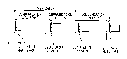
Fig. 4 schematically indicates a structure example of
data in the communication system with employment of the
P1394 serial bus;
Fig. 5 schematically shows a model for packeting AV
data to be transmitted in the communication system with
employment of the P1394 serial bus;
Fig. 6 schematically represents such a condition that
the data block is dropped out when the cycle start data is
dropped out in the communication system of Fig. 5;
Fig. 7 schematically represents such a condition that
the data block is transmitted when the cycle start data is
dropped out in the communication system of Fig. 5;
Fig. 8 schematically indicates an example of an AV
communication system with employment of the P1394 serial
16
2149837
bus, according to an embodiment of the present invention;
Fig. 9 is a schematic diagram for showing an
arrangement of an AV appliance employed in the AV
communication system of Fig. 8;
Fig. 10 schematically indicates an example of a
communication cycle employed in the AV communication system
of Fig. 8; and
Fig. 11 is an explanatory diagram for explaining a
sequence to allocate node IDs employed in the communication
system with employment of the P1394 serial bus.
DETAILED DESCRIPTION OF THE PREFERRED EMBODIMENTS
Referring now to drawings, a communication system
according to an embodiment of the present invention will be
described in detail.
Fig. 1 schematically shows a transmission example of a
data block in the communication system according to the
present invention.
It should be noted that Fig. l(a) indicates a data
block arrives to a transmitter circuit, Fig. l(b) shows a
packet transmitted from the transmitter circuit, and Fig.
l(c) denotes the number of the last data block transmitted.
In the present invention, such an idea is introduced
that ~m~ximum data block number" and ~Max Delay" are
employed so as to represent a relationship between a data
17
21498~7
block arrived to the transmitter circuit and a data block
within a packet transmitted from the transmitter circuit.
The m~ximum data block number corresponds to a m~ximum
value of a data block number which can be transmitted by a
single packet. This m~ximum data block number is set to
such a value which is greater than the m~Ximum block number
of data arrived to the transmitter circuit within 125
microseconds corresponding to a cycle sink period. In Fig.
1, since the data block arrives to the transmitter circuit
in an interval of approximately 24 microseconds, this
m~Ximum number is set to 6 whereas the m~ximum data block
number is set to 7.
The Max Delay corresponds to a m~ximum value of delay
time defined after the data block has arrived to the
transmitter circuit until this data block is sent out. In
case of Fig. 1, the Max Delay is equal to 250 microseconds.
As to a data block transmitted within one
communication cycle, such data blocks which have not yet
been transmitted are combined into a single packet and this
single data packet is transmitted among data blocks which
have arrived from a cycle sink just before a time instant
when cycle start data is received up to the Max Delay. It
should be noted that the number of data blocks does not
exceed the m~xi mum data block number. Since the number of
data block which is finally transmitted is stored, it may
18
~ 21~9837
be recognized which data blocks have been transmitted.
In case of Fig. 1, data blocks up to the data block
"O" are transmitted in the communication cycle m-2, the
data blocks "l" to "6" are transmitted in the communication
cycle m-l, the data blocks 7 to 11 are transmitted in the
communication cycle m, and the data blocks 12 to 16 are
transmitted in the communication cycle m+l.
Fig. 2 schematically shows a transmission example when
cycle start data is dropped out in accordance with the
present invention. It should also be noted in Fig. 2 that
an interval of data blocks arrived to a transmitter
circuit, the m~ximum data block number, and Max Delay are
identical to those of Fig. 1. Similarly, data blocks up to
a data block "O" are transmitted in the communication cycle
m-2 same as in Fig. 1. However, since the cycle start data
m-l is dropped out in this drawing, the data blocks 1 to 6
cannot be transmitted in the communication cycle m-l.
Thus, these data blocks 1 to 6 are transmitted in the
co~munication cycle m commenced from the cycle start data
m. Then, as seven data blocks can be transmitted as a
single data packet at maximum in this embodiment, the data
blocks 1 to 6 and the data block 7 are combined with each
other to form a single packet which will then be
transmitted. Similarly, in the next communication cycle
m+l, data blocks 8 to 14 are transmitted. Subsequently,
19
214g837
such data blocks which have not yet been transmitted are
combined with each other as a single packet and this single
data packet is transmitted among the data blocks which have
arrived from the cycle sink immediately before the cycle
start data is received up to the Max Delay.
It should be understood that although the Max Delay is
set to twice as the interval of the cycle sink in the
above-described embodiment, the Max Delay may be made
longer than the interval of the cycle sink if it is not
required to prevent the drop out of the data block when the
cycle start data is dropped out. Conversely, when the data
blocks are not dropped out even when more than two cycle
start data are continuously dropped out, the Max Delay
should be selected to be three times longer than the
interval of the cycle sink.
Also, it should be noted that although the m~xi mum
data block number is set to be such a number (=7) larger
than the m~ximum number (=6) of data blocks by 1 which
arrive to the transmitter circuit within one cycle sink in
the above-described embodiment, the m~ximum data block
number may be set to be larger than 2.
Furthermore, although the m~xi mum value of the data
~locks which have arrived to the transmitter circuit within
1 cycle sink in the above-described embodiment is selected
to 6, the present invention may be applied to such a system
21~g~3~
that the m~xi mum value of the data blocks arrived to the
transmitter circuit within 1 cycles sink is larger than, or
equal to 1.