Note : Les descriptions sont présentées dans la langue officielle dans laquelle elles ont été soumises.
/C ~~ ~ ~ .~i ~~, / 21 ~ 0 319
. C...
1
n r 1 i m n f r r' i r 'n n
electric ~aower line
TECHNICAL FIELD
The present invention relates to control equipment for a
series capacitor connected into an electric power transmission
line, the equipment having
- a semiconductor valve, which is controllable in both direc-
tions, for connection in parallel with the capacitor, an in-
ductor arranged in series with the capacitor and the semi-
conductor valve, forming an oscillating circuit together with
the capacitor, and
- control members adapted to influence the firing times of the
semiconductor valve for controlling the capacitor voltage.
BACKGROUND ART
In electric power networks, which comprise thermal power
generating units (turbo-generators) and series-compensated
transmission lines, non-damped and negatively damped oscilla-
tions may occur at a certain unfavourable degree of compensa-
tion. Such oscillations arise through cooperation between on
the one hand the electrical system and on the other hand
mechanical torsional oscillation modes with low damping in the
shaft system of the turbine-generator units. The phenomenon is
referred to as subsynchronous resonance (SSR).
SSR occurs in normal plants for production of thermal electric
power at the frequencies
fm in the mechanical system, and
fN - fm in the electrical system,
where fN is the system frequency of the power network -
normally 50 Hz or 60 Hz - and where in typical plants
15 Hz < fm < 45 Hz
Normally, within this frequency range, three to five different
mechanical resonance modes with varying mechanical damping
' ' ~,,- , _ 2~.~0~19
2
occur in each generator-turbine unit.
SSR oscillations have proved to lead to such great stresses in
the shaft systems that permanent damage or total breakdown
arises. Several methods for damping or for avoiding SSR have
therefore been proposed.
Thus, it is known, for example from Swedish published patent
application 446 289, to arrange damping resistors which are
permanently connected or which are switched in when SSR are
detected. Such resistors, however, will have large dimensions
and possibly also a high power consumption and are therefore
expensive and space-demanding.
It has therefore been proposed to design the series capacitor
controllable and controlling it in such a way that a damping
of SSR is obtained. From Swedish published patent application
465 596 such series capacitor equipment is previously known.
The equipment has measuring and filtering members adapted to
detect the occurrence of an SSR oscillation and to form a
quantity corresponding to the SSR oscillation. This quantity
is supplied to control members adapted to control the semicon-
ductor valve in such a way that a damping of SSR oscillations
arising is obtained. In this way, in principle, a damping of
SSR oscillations, free of losses, may be achieved, and this
only by a suitable design of the control members of the series
capacitor. In practice, however, it has proved to be difficult
to isolate an SSR component from measured operating quantities
of the power line or the capacitor in an acceptable way, since
this component should be capable of being detected even at a
low level. An additional difficulty is that the frequencies of
all the oscillating modes for subsynchronous oscillations,
which may become critical at some connection state (a certain
configuration of the lines) in the network, must be known in
advance. Critical modes depend on which lines are connected or
disconnected, which generators are connected, and which series
capacitors are connected at a certain time.
210319
' ~,.,w _
3
US patent 5 202 583 describes a device of the kind stated in
the introductory part of this specification for fast fine
control of a series capacitor connected into a power line. By
a predicting control of the firing times of the semiconductor
valve, a desired addition to the capacitor voltage may be
rapidly set and maintained. The described system is probably
capable of damping such subsynchronous electric oscillations
which are caused by transient phenomena. However, the system
becomes dependent on a plurality of internal and external
parameters and cannot, therefore, under the operating condi-
tions which are often varying in practice, effectively prevent
the occurrence of subsynchronous resonance oscillations (SSR
oscillations).
European patent application with publication number 0 571 642
describes a thyristor-controlled series capacitor which may be
bridged by a surge arrester or by an electric switching
device. The publication describes how an internal synchroniza-
tion signal for control of the thyristors may be obtained and
maintained also in case of a bridged state of the capacitor.
SUMMARY OF THE INVENTION
The invention aims to provide simple and, in principle, loss-
less equipment of the kind described in the introductory part
of the description, which efficiently damps or completely
prevents subsynchronous resonances independently of variations
in the operating conditions or network data, and which at the
same time makes possible a control of the effective impedance
of the series capacitor at the system frequency, which is
independent of the SSR oscillation.
In equipment according to the invention, the semiconductor
valve is controlled in such a way that the apparent impedance
of the series capacitor equipment within the whole range in
which SSR oscillations may occur becomes inductive instead of
capacitive. It has been found that this can lead to SSR
oscillations being effectively damped or completely elimi-
CA 02150319 2001-09-21
4
nated.
According to the present invention, there is provided a
control equipment for a series capacitor connected into an
electric transmission line for carrying a current having a
fundamental component having a fundamental tone frequency,
said equipment comprising:
- a semi-conductor valve and an inductor connected in
series with each other and in parallel with said capacitor,
said semi-conductor valve being controllable i~z both
directions, and said inductor forming, together with said
capacitor and said semi-conductor valve an oscillating
circuit in which the capacitor has a voltage exhibiting
periodic zero-crossing times;
- control members responsive t:o the current in the
transmission line and voltage across the capacitor for
firing the semi-conductor valve at controllable firing
times such that the periodic zero crossing times of the
capacitor voltage are substantially equidistant, thereby
causing the apparent impedance of the oscillating circuit
to appear inductive with respect to line current components
having a frequency below the frequency of the fundamental
component;
- means producing equidistant start pulses as a function
of the phase of the line frequency;;
- means for producing a firing time signal for firing
the semi-conductor valve in dependence on the line current
and the capacitor voltage such that the time between the
start pulses and zero crossings of the capacitor voltage
becomes substantially constant.
Preferably, this is achieved according to the invention by
controlling the semiconductor valve in such a way that the
zero crossing of the capacitor voltage remain equidistant
during processes when the line current contains, besides
its fundamental component, subsynchronous components. In
this way, the series capacitor equipment will
CA 02150319 2001-09-21
4a
systematically exhibit an inductive character within the
whole frequency range which is of interest for S~3R, and
this is true independently of the control state of the
capacitor, independently of the characteristics of the
power line or the power network, and independently of the
magnitude of the fundamental component of the current in
the power line.
Preferably, in one embodiment of the invention, the
control members comprise a command-signal-generating
member, preferably a phase-locked circuit synchronized to
the power line current and adapted to supply equidistant
command signals which are substantially independent of SSR
components and which are used as reference when initiating
the firing of the semiconductor valve. Each firing of the
semiconductor va7_ve causes a recharge of the capacitor, and
the recharge time is dependent on the values of the
capacitor voltage and the line current at the time of
firing. A ca7_culating circuit is then adapted, in
dependence on the capacitor voltage and the line current,
to determine the firing time such that the zero crossings
of the capacitor voltage always occur at a certain fixed
time after the command signal.
Preferably, according to one embodiment of the invention,
a superordinate control member is adapted for controlling
the fundamental component of the capacitor voltage. The
superordinate control member then comprises members adapted
to form a state quantity, which is dependent on the
addition to the capacitor voltage which i.s achieved by the
effect of the semiconductor valve, and, in dependence on
the difference between the state signal and a reference
value, to control the times for the zero crossings of the
capacitor voltages. In this way the
CA 02150319 1998-10-22
invention provides a possibility of control of the effect of
the series capacitor at the system frequency, that is, the
degree of compensation, and this while at the same time the
advantageous SSR damping according to the invention is all the
time active.
BRIEF DESCRIPTION OF THE DRAWINGS
The invention will be described in greater detail in the
following with reference to the accompanying Figures 1-11,
wherein
Figure 1 shows the main components of controllable series
capacitor equipment of the kind to which the
invention relates,
Figure 2 shows voltage and current plotted against time in
equipment according to Figure 1,
Figure 3 shows current and voltage during a voltage reversal
period,
Figure 4 shows an idealized picture of the voltage and_
current of the capacitor at a certain control-state,
Figure 5 shows as a background to the derivation of the
apparent impedance of the equipment how the times of
sampling of the capacitor voltage lie in relation to
the firing times of the capacitor voltage,
Figure 6 shows how the apparent impedance of the capacitor
equipment varies with the frequency within the
subsynchronous frequency range,
Figure 7 shows the principle of control equipment according
' 2150319
to the invention,
6
Figure 8 shows as a function of time in connection with a
firing of the semiconductor valve, the command
signal and the current through the semiconductor
valve,
Figure 9 shows the function of that part of the control
equipment which determines the time of firing of the
semiconductor valve,
Figure 10 shows an alternative embodiment of equipment
according to the invention, wherein a control system
is adapted for control of the control state of the
capacitor equipment, and
Figure 11 shows an alternative embodiment of the control
equipment, wherein the control state of the
capacitor is normally low but is increased when
there is a need of SSR damping.
DESCRIPTION OF THE PREFERRED EMBODIMENTS
Figure 1 shows a series capacitor 1 connected into an electric
power line 2. For the sake of simplicity, this figure and the
following figures show and describe single-phase lines and
capacitor equipment.
In the power line flows the current iL, which is determined by
the power line and the network of which it is part. The
voltage across the capacitor is designated uC. The system
frequency of the power network is fN = ~ and is normally 50
Hz or 60 Hz. At the system frequency, the capacitor has the
capacitive reactance xc = 1 where C is the capacitance of
(~N.C
the capacitor.
~.
214319
In parallel with the capacitor, control equipment CE is
connected for control of the capacitor. The control equipment
comprises a semiconductor valve 3 which is controllable in
both directions and which is series-connected to an inductor
4. In the embodiment shown, the semiconductor valve 3 consists
of two antiparallel-connected thyristors 3a and 3b.
The inductor 4 has an inductance L and hence, at the system
frequency, an inductive reactance xv = c~N~L. The inductance L
of the inductor 4 is so chosen in relation to the capacitance
of the capacitor 3 that xv < xc, which means that the natural
frequency of the oscillating circuit formed by the capacitor
and the inductor is higher, preferably considerably higher,
than the system frequency of the network. Typical values of
the natural frequency of the circuit fall within the range 2.5
- 5 times the power frequency.
In steady state, the semiconductor valves are conducting in
intervals which symmetrically surround the zero crossings of
the capacitor voltage. Figure 2 schematically shows the
capacitor voltage uc, the line current iL and the valve
current iV plotted against time t. At, for example, the zero
crossing at which the capacitor voltage changes signs from a
negative to a positive sign, the semiconductor valve (valve
3b) is fired at the time tF and a current pulse iV traverses
the circuit formed by the capacitor, the inductor and the
semiconductor valve. At t = tE, the current through the
semiconductor valve becomes zero, and the valve expires.
Figure 3 shows in more detail the variations with time of the
quantities u~, iL and iV in connection with the zero crossing
of the capacitor voltage. The semiconductor valve is fired at
t=tg and the capacitor voltage u~ then has the value u~0. If
the losses are neglected, the capacitor voltage has, at the
end of the conduction interval of the valve, that is, at t=tE,
the value -u~p. The voltage is then as great as the voltage at
the beginning of the conduction interval but has the opposite
polarity. The function of the control equipment is thus to
2150319
8
reverse the instantaneous voltage of the capacitor. As is
clear from Figure 3, this means an addition Dus (sometimes
called voltage boost) to the change of the capacitor voltage
during the interval tF to tg in addition to what is caused by
the line current during the same interval. By suitable control
of the semiconductor valve, the capacitor voltage may be con-
trolled in this way. Allowing the firing time fF to occur
earlier gives an increased value of the quantity Dus, which
may be expressed as an increasing control state of the capa-
citor. The quantity Dus may be considered a measure of the
control state of the capacitor, and an increase of Dus gives
an increase of the capacitor voltage and of the effective
impedance of the capacitor at the system frequency.
Since the reversal of the capacitor voltage takes place at the
peak value of the line current, and since the time of the
reversal is short in relation to half the period of the line
voltage, the line current iL may be considered to be approxi-
mately constant during the voltage reversal process and is
shown as a straight line in the figure.
The time integral (the current time area) of the valve current
iv during the reversal process is qv and it is this charge
quantity that gives the capacitor the above-mentioned voltage
addition Dus.
In practice, unavoidable losses in the reversal circuit occur.
Taking these losses into consideration, the following may be
set
u~(tE) - -D~u~(tF)
where 0 < D < 1 is a factor which characterizes the factor of
merit of the circuit. The factor D is, in practice, relatively
near the value 1 and may, in practice, be considered to be
within the interval 0.90 - 0.95.
When reducing the inductance in that thyristor-controlled
inductive branch, which is connected in parallel with the
series capacitor, the conduction interval of the thyristors
21~031~
9
will become increasingly shorter and the peak value of the
thyristor current increasingly greater. However, the function
to reverse the voltage remains unchanged. It proves that the
function "reversal of the capacitor voltage" is a suitable
starting-point of the derivation of the interaction between a
thyristor-controlled series capacitor and the transmission
system in which the capacitor is included.
For analysis of the function of the circuit, in many cases the
voltage reversals may be regarded as instantaneous
(corresponding to the inductance zero). If such indealized
series capacitor equipment is operating on a transmission line
with a certain current, the voltage reversals will, in steady
state, occur at the zero crossings of the series capacitor
voltage and with a frequency which is twice the power
frequency.
Figure 4 illustrates the function of such idealized series
capacitor equipment. The instantaneous reversal of the
capacitor voltage takes place at t=t0, that is at the natural
zero crossing of the capacitor voltage (and at the peak value
of the line current). The reversal gives the addition (the
voltage boost) Dus to the capacitor voltage u~.
An infinitesimal alternating current
0i ( t ) - ~i cos S2t = Re [0i e3~t ]
with the angular frequency S2, superimposed on the stationary
line current, produces an additional voltage Du across the
series capacitor. This additional voltage contains a component
with the frequency SZ, which may be represented as
Du(t) - 0u cos(SZt+O) - Re [Du e~~ e~~t]
The quotient
Du e70
z(~) - Di
is then a measure of the apparent impedance which the capa-
citor equipment (capacitor with associated control equipment)
2mo319
,. , ~ ~ _
exhibits for applied voltages with the angular frequency 52. An
expression for Z(S2) will be derived in the following.
The derivation is performed in the simplest manner for a dis-
crete system in which the voltage is sampled at times tk,
tk+1~ tk+2, etc. The sampling times are located midway between
the times when the voltage reversals occur (the voltage at a
sampling time is then a good measure of the mean value of the
additional voltage during the half-period in question). Figure
10 5 shows the sampling times tk, tk+1. tk+2. The duration of the
sampling interval is h, that is, tk+1-tk = h. The voltage
reversals occur midway between the sampling times, that is, at
tk+h/2, tk+1+h/2, etc., and are symbolically shown in the
figure as short current pulses.
If the quantities are represented by their normalized values
(pu values; per-unit values) the following differential
equation applies to the capacitor voltage as a function of the
line current in the interval between the reversals
1 .
- ~Du=xC-~i
~N
where (~N is the angular frequency of the network. The
following is thus obtained
Du = c~N~xyRe[Di-e7~t]
The duration of the sampling interval is
h - 1 __ n
2fN wN
The integration in the interval
tk < t < tk + h/ 2
then gives
tk+h/2
t~u(tk + 2 - 0) - Du(tk) + laN-xC- JRe[~i-e~~~]d~ }
tk
At the time t=tk, the capacitor voltage is reversed. The
following is then obtained
210319
11
tk+h/2
~u(tk + 2 + 0> - -D~ {~u(tk) + coN~xC~ JRe[Di~e~~~]d~ }
tk
where the factor D, as mentioned above, represents the losses
of the circuit. Renewed integration, now in the interval
tk + h/2 < t < tk+1 = tk + h
gives
tk+h/2
~u(tk + h) - -D~{Du(tk) + c~N-XC~ JRe[~i~e~~~]d~ } +
tk
tk+h
+ c~N xC~ Re(OWe~~~]d~ _
tk+ /2
- -D~Du(tk) +
h/2
+ c~N~xC~Re{4i' (-D + ej~h/2) .ejS2tk. Re(Di~e~~~ld~ } -
0
- - D~Du(tk) + ~N~xC~Re{Di (e~S2h/2 _ Dj~(ejSZh/2 _ 1) ejS2tk}
Now, if Du(tk) is represented according to
Du(tk) - Re{~We~e~e~~tk}
the following equation is obtained
Du~ej9. (ejS2h + D) - ~ ~ (-jxC) ~ (ejS2h/2 _ D) ~ (e7~h/2 _ 1) ~~i
The apparent impedance then becomes
z (SZ) - DW eke - c~N . (_jxC) _ (ejS2h/2 _ D) (ejS2h/2 _ 1)
Di SZ (ejS2h/2 + D)
ujN (e~ (SZ/~)'~/2 _ D) . (ej (SZIwN)~c/2 _
(-jxC). 1)
(e7 (SZ/wN)~ + D)
_ 21503.9
~,..
12
When the capacitor circuit is free of losses, D=1 and the
expression is simplified to
S2 ~
1 - cos
z (S2) - ~ ~ jxC ~ -
cos -
~N
from which expression it is clear that for this case the
apparent reactance becomes inductive within the whole range S2
< wN, that is, for the whole frequency range where subsyn-
chronous resonance may occur. Further, it is clear that the
apparent resistance is zero.
In practice, the losses of the equipment cannot simply be
neglected. Figure 6a and Figure 6b, however, show the
apparent reactance and the apparent resistance,
respectively, for two assumed values of the circuit losses,
namely, for D = 0.90 and for D = 0:95, which together with
the case treated above, D = 1, cover the entire range of
variation of the quantity D which is likely to occur in
practice. The calculations are made for the system frequency
60 Hz, that is, for c~N = 2n~60 and for the frequency range 0
< S~ < 50 Hz and thus cover with a good margin that frequency
range 15 Hz < S2 < 45 Hz where subsynchronous resonance may
occur. Figure 6a shows the quotient xv/xc where xv is the
apparent reactance and xc = 1 .
cy C
Figure 6b shows the quotient rv/xc where rv is the apparent
resistance. As is clear from the curves, the apparent
reactance xv is positive, that is inductive, within the entire
frequency range in question.
The above section thus shows that a thyristor-controlled
series capacitor, in which the capacitor voltage is reversed
at equidistant times, exhibits an inductive characteristic
within the whole range which is of interest to subsynchronous
resonance oscillations. However, the derivation is made on the
assumption that the inductance of the inductor is so low that
2150319
~,.r _
13
the reversal of the capacitor voltage takes place in a negli-
gibly short time.
In practice, the above-mentioned inductance cannot be neglec-
ted, and the voltage reversal will then not take place
instantaneously. The conduction interval of the semiconductor
valve will'have a finite duration, which is dependent on the
relationship between on the one hand the voltage of the capa-
citor upon firing of the valve and on the other hand the value
of the line current during the conduction interval of the
valve, and on the natural frequency of the LC circuit which is
constituted by the series capacitor and the inductance of the
branch. It can, however, be shown that, if the control of the
firing of the valve is modified such that the time of the zero
crossings of the capacitor voltage is maintained independent
of variations in these variables, the apparent impedance will
maintain its inductive character.
The derivation above has been made solely on the basis of the
principle of equidistant voltage reversals, and no system
parameters, such as line impedances, etc., occur in the
relationships. Thus, the curves in Figure 6a and Figure 6b
apply independently of the transmission system and of the
magnitude of the fundamental current component.
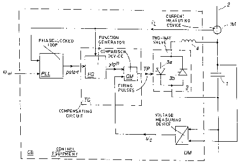
Figure 7 shows the fundamental configuration of control equip-
ment CE according to the invention, which is connected to a
series capacitor 1, connected into a power line 2, for control
of the capacitor. The control equipment comprises a two-way
.valve 3 and an inductor 4, which, connected in series with
each other, are connected in parallel with the capacitor 1. A
current measuring device IM, for example a current transformer
or a current measuring device with optical signal transmis-
sion., is connected into the power line and delivers a measured
signal iL' to the control equipment corresponding to the line
current iL. A voltage measuring device UM, for example a vol-
tage divider with optical signal transmission or a voltage
transformer, is connected across the capacitor and delivers a
~1~0319
. : ~. _
14
measured signal uC' corresponding to the capacitor voltage uC.
The control equipment comprises a phase-locked circuit (Phase-
Locked Loop) PLL, which by the signal iL' is synchronized with
the line current iL. The circuit supplies equidistant command
pulses pstart with a frequency which is twice the system
frequency of the network in which the power line 1 is inclu-
ded. The phase position of the command pulses in relation to
the line current iL is determined by a phase reference signal
eref. This signal is obtained preferably from a superordinate
control system, which controls the properties of the series
capacitor equipment at the fundamental tone of the system
frequency (see more detailed description below with reference
to Figure 10).
The phase-locked loop PLL is provided with suitable filter
means to limit or eliminate the effect of the subsynchronous
currents. The bandwidth of these filter means may be made so
low that the subsynchronous components are practically
entirely eliminated, but in practice it has proved to be
advantageous to have a relatively high bandwidth. The filter
means may, for example, consist of a low-pass filter arranged
in the signal path of the phase-difference signal formed in
the phase-locked loop.
The command pulses pstart are supplied, as are the measured
signals uC' and iL', to a compensating circuit TC. Based on
the measured instantaneous values of capacitor voltage and
line current, this circuit corrects the varying delay (between
the firing of the thyristor valve and the zero crossing of the
capacitor voltage) which arises because of the finite reversal
time of the thyristor-inductor-capacitor circuit. The compen-
sating circuit delivers firing pulses TP to the thyristor
valve.
It can be shown that the duration t1 of the conduction
interval of the thyristor valve is determined from the
relationship
~'~w t1 = 2'~
;,~.,~' ~2150319
where
~, = xc / xv
= arctan -uco
(xciL) /~
and -uCp is the capacitor voltage at the moment of firing.
As will be clear from Figure 8, the following applies for the
time tdp between the firing of the valve at t = tF and the
peak value of the current at t = tp
10 tdp = t1/2
that is,
tdp =
~'~N
The time tdp will have its highest value tdpp at a high
capacitor voltage and/or a low line current, and the quantity
~, then has its greatest value Amax= ~/2, that is,
n/2
tdpo a,O~N
According to the invention, the zero crossings of the
capacitor voltage, that is, the times of the maximum values of
the valve current, shall be equidistant, that is,
tp = tstart + tdp0
From these conditions, the relationship is obtained which
defines the firing time tF:
xcz ~ tF) tan [2 - ~,t~N(tF-tstart) l - -uc(tF)
The compensating circuit TC includes a function generator FG
which is adapted, in dependence on the magnitude of the line
current and starting at each starting pulse pstart~ to
generate a function
yfg(t) _ xcl~(t) tan [2 - a.ci~N(t-tstart) J
The value of this function is supplied to a comparison device
CM which is adapted to continuously compare this function with
the instantaneous values -uC(t) of the capacitor voltage. At
'. 2150319
.,,~~ _
16
t = tF, the value of the function and the capacitor voltage
are equally great, and the device CM is adapted to then supply
a signal TP for firing the thyristor valve.
The variation of the function yfg(t) and of the capacitor
voltage -uC is shown in Figure 9.
The line current iL, the measured value of which is included
in the above relationships, need not be measured continuously.
The firing of the valve is always performed near the zero
crossing of the capacitor voltage, that is, near the peak
value of the line current. Since the current then varies
slowly, one single sampling of iL, for example at t = tstart~
may provide sufficient accuracy for determining tF. The
determination of the firing time may, if desired, be refined
by correcting the measured value of the line current taking
into account the normally sinusoidal variation of the line
current.
In the control method described above with reference to
Figures 7-9, the voltage reversals (the zero crossings of the
capacitor voltage) of the capacitor will always occur at
equidistant times given by the phase-locked loop, indepen-
dently of the magnitude of the capacitor voltage, that is, of
the control state of the capacitor. Steady state occurs if the
total net charge, supplied by the line current to the
capacitor between two voltage reversals, is zero. If this
condition is fulfilled, the capacitor voltage has the same
value immediately before a voltage reversal as immediately
after the preceding reversal.
If, for example, the zero crossings occur somewhat earlier in
relation to the times which correspond to the steady state,
the line current will, during each interval between two rever-
sals, give a positive net addition to the charge of the capa-
citor, and the capacitor voltage will continuously increase.
If, on the other hand, the zero crossings occur somewhat later
in relation to the times which correspond to the steady state,
_2150319
,, .
17
the line current will, during each interval between two rever-
sals, give a negative net addition to the charge of the capa-
citor, and the capacitor voltage will continuously decrease. A
small deviation of the firing times from the times which
correspond to steady state will thus with an integrating
effect give an increasing or a decreasing control state of the
capacitor. The control equipment shown in Figure 7 is there-
fore supplemented, according to a preferred embodiment, by a
superordinate control circuit which maintains the capacitor
voltage, that is, the control state thereof, at the desired
level.
Figure 10 shows such control equipment. A second current
measuring device IMV delivers a measured signal iv' corre-.
sponding to the valve current iv. This signal is supplied to a
charge measuring device QM. In this device, by integration of
the valve current during the reversal process, a signal q is
formed which corresponds to the time integral of the valve
current, that is, the change of the charge of the capacitor
and hence of the voltage thereof, caused by the reversal. The
quantity q is thus a measure of the control of the capacitor
(cf. Figure 3 with associated description). To eliminate such
components in the measured signal as are caused by subsyn-
chronous resonance phenomena, the measured signal q is passed
through a low-pass filter LP with such a selected characte-
ristic that components of SSR frequency are eliminated. In a
summator S1 the filtered signal q' is compared with a refe-
rence signal qref which is obtained from a superordi.nate con-
trol system SR and which constitutes a reference for the con-
trol state of the capacitor. The deviation ~q is supplied to a
regulator QR, the output signal tcs of which in turn is supp-
lied to a time-delay circuit TF, which delays the pulses
Pstart obtained from the phase-locked loop proportionally to
the output signal of the regulator and in such a way that a
positive value of 0q results in the firing times occurring
earlier and negative value results in the firing times occurr-
ing later. The amplification of the circuit TF is influenced
by the amplitude of the line current and is, for example, in-
~. ..
_ 21503.9
18
versely proportional to the absolute value of the line
current. Because of the above-mentioned inherent integrating
function of the system, the regulator QR may be a pure propor-
tionality regulator. In practice, however, it has proved to be
suitable to design the regulator as a PI regulator with a
smaller integrating part, among other things to compensate for
the effect of circuit losses. In this way, that capacitor
voltage/control state which is given by the reference value
qref is automatically obtained and maintained. The pulses
obtained from the time-delay circuit TF are designated
P~start-
The superordinate control system SR is not part of the inven-
tion but may be a regulator or control equipment for control
of the power system in which the power line and the series
capacitor in question are included. The signal qref may thus
be varied by the superordinate system, for example in depen-
dence on the desired SSR damping, for damping electromecha-
nical low-frequency oscillations in the network, for controll-
ing the power flow in the network, or quite simply for setting
a certain desired reactance in the series capacitor.
In certain cases, there is no wish to use the control of the
series capacitor for any other purpose than to counteract SSR
oscillations. The control state of the capacitor (the voltage
boost) may then be adapted only in view of what is required
for this purpose. In general, it is then desirable to maintain
the control state as low as possible to reduce the harmonics
in the capacitor voltage and to reduce the thermal stresses on
the semiconductor valves and on the capacitor. To counteract
an SSR oscillation, however, a certain lowest level of the
capacitor voltage is required. According to one embodiment of
the invention, therefore, the control system is designed such
that, during undisturbed operation, it maintains the control
state at a very low value - possibly zero - but, on the
occurrence of an SSR oscillation, if need arises, raises the
control state to a sufficient degree for the system to give
the desired SSR damping.
210319
;~ w _
19
As is clear from Figure 9, for low capacitor voltages, no
intersectional point is obtained between the curve -uC(t) and
the curve yfg(t) during the interval tstart - tp and, there-
fore, no firing of the semiconductor valve. To obtain the
desired control function with equidistant zero crossings of
the capacitor voltage, the control state and hence the capa-
citor voltage must be so high that an intersectional point is
obtained during the time interval mentioned.
Figure 11 shows additional equipment which, together with the
equipment shown in Figure 10, provides the above-mentioned
function. The pulses pstart from the phase-locked loop PLL are
supplied to a delay circuit FC with the time delay tdp0 and
this circuit delivers the pulses pp at the times tp for the
desired equidistant zero crossings of the capacitor voltage
uc. The pulses are supplied to an input of an AND circuit AG.
The firing pulses TP from the compensating circuit TC are
supplied to a monostable flip-flop MV with the return time
tdpp. The flip-flop thus delivers signals ptp+ starting in
20. each received firing pulse and with the duration tdp0. These
signals are supplied to a negative input of the AND circuit
AG. If the capacitor voltage is so low that no intersectional
point has been obtained between -uc and yfg, the signal ptp+
is zero at t = tp, and the AND circuit delivers a pulse ~qref+
with a suitable amplitude which is supplied to a regulator DQR
with PI function. The output signal Oqref of the regulator is
supplied to the summator S1 in Figure 10 and is assumed to be
zero. The input signal qref to the summator has the value
which corresponds to the control state desired during undis-
30 turbed operation, thus preferably zero or a low value. The
pulse ~qref+ provides an instantaneous positive addition to
the output signal of the regulator, which addition acts as an
instantaneous increase of the reference qref bY the amount
~qref. If no intersectional point is obtained after the next
pulse pstart either, and hence no firing pulse, the increase
of qref is repeated until firing pulses are obtained and hence
the desired SSR-damping control of the capacitor. A weakly
negative signal ~qref- is supplied to a second input of the
. , ~- _ 215 0 319
regulator DQR and provides, because of the integrating com-
ponent of the regulator characteristic, a slow reduction of
the reference voltage addition ~qref. which causes this addi-
tion to be reduced to zero after cessation of an SSR oscilla-
tion.
As shown above, with the aid of control equipment according to
the invention, series capacitor equipment connected into a
power line may be caused to exhibit an inductive impedance
10 within the entire frequency range where SSR oscillations may
occur. This means that the power line vis-à-vis the remainder
of the network operates, from the SSR point of view, as an
uncompensated line, and hence SSR oscillations will be
efficiently counteracted. This advantageous function is
obtained independently of electrical data of the power line
and the surrounding network. The efficient SSR damping
therefore becomes independent of variations in the configura-
tion and data of the line or the remainder of the power net-
work, and since precise knowledge of line or network data is
20 not required, existing series capacitor equipment may be
simply supplemented by control equipment according to the
invention, or existing control equipment by redesigned accor-
ding to the invention. The SSR damping is obtained solely
through control actions, and it is therefore, in practice,
free of losses. These advantages are obtained while at the
same time a rapid and lossless control of the effective capa-
citance of the capacitor equipment at the system frequency of
the network is made possible.
The embodiments of the invention described above are only
examples, and control equipment according to the invention may
be designed in a plurality of alternative ways.
Thus, the inductor 4 may be connected into the power line 2 in
series with the capacitor 1, the semiconductor 3 thus being
connected in parallel with the series connection of the induc-
tor and the capacitor. As shown in Figures 2 and 3 in the
Swedish published patent application 465 596 mentioned above,
_ 2i~~~~~
21
an inductor may be connected in series with each one of two
oppositely directed parallel-connected semiconductor valves,
or the semiconductor valve or both the valve and the inductor
may be connected to the capacitor with the aid of a trans-
former for adaptation of the voltage and current levels of
these components.
In the examples described above, the semiconductor valve
consists of two antiparallel-connected thyristor valves
equipped with conventional thyristors. Alternatively, the
semiconductor elements included in the valves may consist of
other semiconductor elements, for example gate turn-off
thyristors (GTO thyristors) or high-power transistors.
For the sake of simplicity, only single-phase designs of
control equipment according to the invention are described
above. However, the invention is primarily intended for use in
three-phase power transmission lines. Each phase of the line
may then be provided with separate control equipment of the
kind described above, in which case the control members for
control of the firing of the semiconductor valves may to a
greater or lesser extent be common for the three phases.
The control members for control of the firing of the semicon-
ductor valves may be designed in many other ways that those
described above. Suitably, at least certain parts, for example
the function generator FG in Figure 7, may consist of an
appropriately programmed microprocessor or computer.
The quantities, for example the capacitor voltage, the line
current and the reversed capacitor charge, which are used for
control of the series capacitor may be obtained in other ways
than what is described above. Generally, these quantities may
be formed or calculated from other measured quantities. The
above embodiments thus show how the capacitor voltage is
measured directly across the capacitor. Alternatively, this
voltage may be measured across the semiconductor valve, the
voltage of which prior to firing of the valve is identical
. . ._
' ~ 215~3~9
22
with the capacitor voltage. Instead of forming a measure of
the reversed charge q (and hence the control state) by inte-
gration of the valve current, as described above, this charge
may be determined by measuring the difference between the
capacitor voltage before and after the reversal and by sub-
tracting, from the capacitor charge corresponding to this
voltage difference, the charge addition provided by the line
current during the voltage reversal interval.
In the embodiments described above, the control equipment
according to the invention is connected across the whole
series capacitor. A series capacitor comprises in a known
manner a large number of series- and parallel-connected
capacitor elements, and these may be regarded as constituting
two capacitors connected in series with each other. Control
equipment according to the invention may be connected in
parallel with only one of these parts, which makes possible a
narrower dimensioning of the control equipment. Through the
control, an inductive characteristic within the SSR range is
then only attained in this part, whereas the other capacitor
part has a purely capacitive characteristic both at the system
frequency and within the SSR range. The reduction of the total
capacitive impedance which is obtained in this way may,
however, be sufficient to counteract SSR oscillations to the
desired extent.
With reference to Figure 10 above, a regulator has been
described which controls the additional voltage which is
achieved by the reversal of the capacitor charge. Alterna-
lively, the total voltage of the capacitor may be controlled,
that is, the sum of the additional voltage and the capacitor
voltage caused by the line current.