Note : Les descriptions sont présentées dans la langue officielle dans laquelle elles ont été soumises.
WO 95/13663 2 1 5 2 8 ~ O PCT/U594/11290
EMBEDDED TRAN~MT~ ION LINE COUPLER
FOR RADIO FREQUENCY SIGNAL AMPLIFIERS
B~(~k~round of the Invention
The present invention is generally related to radio
frequency (RF) signal couplers, and more particularly to an
embedded tr~n~mi~sion line coupler for RF signal amplifiers
of cellular telephones.
In conventional cellular telephones, RF signal couplers
have been implemented by several methods, including by
means of capacitive couplers or tr~n~mi~sion line couplers.
Prior tr~n~mi.~ion line couplers typically have been designed
to be termin~te-l by fifty ohm loads at all ports. As a result, it
is necess~ry to include circuitry in the output of an RF signal
amplifier that provides a match to a fifty ohm load. Such
output matching circuitry usually includes one or more
tr~n~mission lines and several capacitors, resistors and/or
inductors, all of which require valuable circuit board space.
Furthermore, the overall insertion loss between the RF signal
amplifier and the antenna includes losses due to both the
output m~t~hing circuitry and the tr~nfimi~sion line coupler.
For the foregoing reasons, there is a need for an embedded
tr~nRmi.~sion line coupler that is integrated into the output
m~t-~hing circuitry of the RF signal amplifier.
P~rief Description of the Drawings
FIG. 1 is a block diagram of RF transmitter circuitry
100, which may advantageously utilize the present invention.
FIG. 2 is a block diagram of a cellular telephone 200
including RF transmitter circuitry 100.
FIG. 3 is a detailed circuit diagram of amplifier 103 and
power detect circuitry 109 in FIG. 1.
.
WO 9S/13663 ~ Q - 2 - PCT/US94/11290
FIG. 4 is a section of a circuit board of the transmitter
circuitry in FIG. 1, showing tr~n~mi~sion line coupler 115.
FIG. 6 is a top view of the top layer 321 of the circuit
board section in FIG. 4, showing an embodiment of
5 tr~n.~mi.~sion lines 201 and 202 of tr~n.cmi~ion line coupler
115.
FIG. 6 is a top view of the top layer 321 of the circuit
board section in FIG. 4, showing the preferred embodiment of
tr~n.cmi~ion lines 201 and 202 of tr~n~mi~ion line coupler
10 115. `
FIG. 7 is a top view of the top layer 321 of the circuit
board section in FIG. 4, showing an alternate embodiment of
tr~n~mi~ion lines 201 and 202 of tr~n~mi~ion line coupler
115.
Descril~tion of the Preferred ~mbodiment
Briefly described, the present invention encompasses RF
signal coupler circuitry for detecting an RF signal generated
20 by an amplifier and producing an RF detect sign~l. The
amplifier further has an output coupled to tr~n~mi.~sion line
matching circuitry. The RF signal coupler circuitry
comprises a substrate having top and bottom surfaces and a
predetermined dielectric constant; a through-path
25 tr~n~mi~sion line having a predetermined shape and b~ing
disposed on the top surface of the substrate, the througk-path
tr~n~mi~sion line coupled to the RF signal and included in the
tr~n~mi~sion line m~t~hin~ circuitry of the amplifier; and a
coupled-path tr~nsmission line being disposed on the bottom
30 surface of the substrate and having a coupled port coupled to a
first complex impedance and an isolated port coupled to a
second complex impedance, the coupled-path tr~nfimi~sion
line electrom~gnetically coupled to the through-path
tr~n~mi~.sion line for generating the RF detect signal at the
WO 95/13663 215 2 8 I ~ PCTtUS94/11290
coupled port having an amplitude related to the amplitude of
the RF æi~n~l.
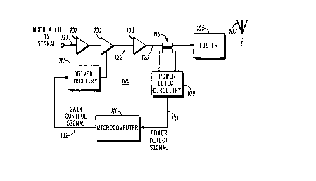
Referring to FIG. 1, there is illustrated a block diagram
of unique RF transmitter circuitry 100, which may
advantageously utilize the present invention. RF transmitter
circuitry 100 is part of cellular telephone 200 in FIG. 2, which
also includes receiver circuitry 141, user interface circuitry
151 coupled to a microphone 152, a speaker 153, and a keypad
154, all of which are controlled by microcomputer 111, and
which may be elements of any conventional cellular telephone,
such as, for example, the cellular telephone shown and
described in Motorola instruction manual number
68P81066E40, entitled "DYNATAC Cellular Mobile Telephone
800 MHZ Transceiver," published by and available from
Motorola C & E Parts, 1313 East Algonquin Road,
S~h~llmburg, Illinois 60196. The operation and features of
such conventional telephone are described in Motorola user's
manual number 68P81116E58, entitled "DYNATAC 6800XL
Cellular Mobile Telephone USER'S MANUAL," published by
and available from Motorola C & E Parts, 1313 East Algonquin
Road, S~h~llmburg, Illinois 60196.
RF transmitter circuitry 100 in FIG. 1 includes
cascaded amplifiers 101, 102, and 103 coupled by directional
coupler 115 and filter 105 to ~ntenn~ 107. RF transmitter
circuitry 100 together with microcomputer 111 and receiver 141
in FIG. 2 may all be implemented on a multi-layer printed
circuit board. Directional coupler 115 iS preferably a
tr~n~mi~sion line directional coupler as described
hereinbelow, and is coupled to power detect circuitry 109,
which produces power detect signal 131. Microcomputer 111 is
responsive to power detect signal 131 for adjusting the
magnitude of gain control signal 132 to produce the desired
power level of transmitter output signal 123. Gain control
signal 132 iS coupled to driver circuitry 113 (which may be
implemented as shown and described in US patent no.
WO 95/13663 2 l S 2 8 1~ PCTIUS94111290 ~
4,523,155, incorporated herein by reference) for adjusting the
voltage/current drive to amplifier 102 to correspondingly
adjust the amplification gain thereof. In analog cellular
telephones, tr~n~mit.ter output signal 123 may be set at one of
5 eight possible power levels in response to control message
from the cellular base st~t.ion~ (see US patent no. 4,523,155).
In digital cellular telephones, transmitter output signal 123
may be set at one of eight possible power levels during an
~si~ned time slot in response to control message from the
cellular base stations (see US patent no. 5,192,223,
incorporated herein by reference). Both analog and digital
cellular telephones may advantageously use the present
invention.
Referring to FIG. 3, there is illustrated a detailed circuit
diagram of final amplifier 103 and power detect circuitry 109
in FIG. 1. A~rlplifier 103 is preferably a field effect tr~n~iRtor
(OKI type KGF1321S FET) which is coupled to amplified 1
signal 122 by a capacitor and tr~n~mi~sion line 203 and
generates the transmitter output signal 123. The output
20 match of amplifier 103 consists of two low pass sections and
harmonic matching for the second and third harmonics. The
harmonic m~trhing is accomplished by tr~n~mi~io~ line 204
and capacitor 243. Tr~n~mi~sion line 205 and capacitor 245
provide one low pass filter section, and tr~n~mi~ion line 201
25 and capacitor 247 provide the other low pass filter section.
Tr~n~mission line 201 is also coupled to filter 105, which is in
turn coupled by two capacitors and an inductor to antenna 107.
According to a novel feature of the present invention,
tr~n~mi~sion lines 201 and 202 are embedded in the output
3~ match of amplifier 103. Since coupler 115 is embedded in the
output match of amplifier 103, the complex impedances at the
coupled port and its isolated port of coupled-path tr~n~mi~ion
line 202 (end connected to inductor 210) need to be carefully
selected such that the signal appearing at the coupled port of
35 coupled-path tr~n~mi~sion line 202 (end connected to inductor
215281~ t
WO 95/13663 PCT~S94/11290
- 5 -
212) includes sign~lq traveling only in the forward direction
and does not include signals traveling in the reverse direction.
In conventional directional couplers, the through-path
tr~nqmiqæion line and the coupled-path tr~nqmiqsion line are
5 designed for fifty ohm impedances at all ports. When ideally
termin~te-l by fifty ohm impetl~nces, a portion of the RF signal
appears at the coupled port of the coupled-path tr~nqmiqqion
line, and no signal appears at the isolated port of the coupled-
path tr~nqmiqfiion line. Also, no reflections of the RF signal
10 occur since the both ports of the through-path tr~nqmiqsion
line are ideally termin~ed by fifty ohm impedances. However,
since through-path tr~nqmi~qion line 201 of embedded coupler
115 iS not ideally termin~tell, but instead coupled between
capacitors 245 and 247, several reflections of transmitter
15 output signal 123 occur.
In coupler 115, a desired portion of transmitter output
signal 123 iS coupled to the coupled port of coupled-path
tr~nqmiqsio~ line 202. Tr~nqmitter output signal 123 travels
down tr~n~miqqion line 201 and a portion is reflected back by
~0 capacitor 247. The first reflected transmitter output signal 123
travels back and a portion is refiectetl back by capacitor 245.
An undesired portion of second reflected transmitter output
signal 123 is coupled to the coupled port of coupled-path
tr~nqmi.qæion line 202. A portion of first reflected transmitter
25 output signal 1 3 is also coupled to the isolated port of coupled-
path tr~nqmiqqion line 202 and travels back to the coupled port
of coupled-path trAnqmiqqion line 202. According to a novel
feature of the present invention, if the proper isolated-port
complex impedance termin~tes the isolated port of coupled-
30 path tr~nqmiq~qion line 202, the portion of first reflectedtransmitter output signal 123 that travels back to the coupled
port will cancel the coupled portion of second refiected
transmitter output signal 123. This proper isolated-port
complex impedance includes a real part and an im.qgin~ry
35 part, which is implemented in the preferred embodiment by
215281Q
WO 95113663 - PCT/US9~/11290
- 6 -
inductor 210 (15 nH) and resistor 222 (39 ohms) coupled in
series to the isolated port of coupled-path tr~n~mi~ion line
202. By utili7:ing the proper isolated-port complex impedance
to cancel l~n~esired portions of the reflected ~ , coupler
115 may be embedded in the output match of amplifier 103,
thereby resulting in subst~nti~l savings in both circuit board
space and the number of components. The proper coupled-
port complex impedance further enhances the desired
cancellation, and is implemented in the preferred embodiment
by inductor 212 (5 nH) coupled in series with inductor 211 (22
nH) and the resistance of diode 206 to the coupled port of
coupled-path tr~n~mi~ion line 202.
Tr~n~mi~sion line 201 provides a through-path for
transmitter output signal 123. Coupled-path tr~n~mi~sion
line 202 is electrom~gnetically coupled to tr~n~mi~ion line 201
for generating an RF detect signal having an amplitude
related to the amplitude of tr~n~mitter output signal 123. The
RF detect signal from tr~n~mi~sion line 202 is coupled by
inductors 212 and 211 to diode 206, which together with
capacitor 231 half-wave rectifies it to generate a DC voltage
proportional thereto that is stored on capacitor 231.
The DC voltage stored on .~p~cit.or 231 is coupled by
resistors 232-235 and capacitor 236 to provide power detect
signal 131. Resistor 224 and diode 207 generate a bias voltage
2~ from voltage V2 which is coupled by resistors 223 and 222 and
inductor 210 to tr~n~mi~sion line 202 for biasing diode 206 via
inductors 212 and 211. Diodes 207 and 206 are preferably hot
carrier diodes having subst~nt.i~lly the same electrical
characteristics, such as, for example, Motorola type
MMBD770T1 diodes. Diode 207 temperature compensates
diode 206 so that power detect signal 131 does not vary with
changes in temperature.
According to a novel feature of power detect circuitry
109, an impedance implemented as inductor 211 (22 nH) is
coupled to diode 206 for m~t~hing the inherent diode resistance
2i~2810
WO 95113663 PCT/US94/11290
- 7-
and c~p~- it~nce (1.5 pF), thereby enhancing the sensitivity of
power detect circuitry 109 by as much as a factor of two.
Although implemented with inductor 211, the ms3tching
impedance may also be implemented by corresponding
5 capacitive circuitry. The matching imper~nce m~imi~es
power transfer to diode 206 and is preferably optimi~e-l for
operation at the low power levels (e.g., at power levels below a
predetermined one of the eight possible power levels), where
sensitivity is most important. Since power detect circuitry 109
10 is more sensitive, less signal is needed for detection and a
coupler 115 with 20 dB of coupling can be used inqte~l of 15 dB
of coupling used in detector circuits without inductor 211.
Coupler 115 with 20 dB of coupling reduces the insertion loss
by apprr~im~tely 0.1 dB, tr~nql~ting into a current drain
15 savings of appro~im~tely 8 mA, thereby substantially
extending the battery talk time.
Referring to FIG. 4, there is illustrated a section of a
circuit board of the transmitter circuitry 100 in FIG. 1,
showing tr~nqmiqsion line coupler 115. Transmitter circuitry
20 100 is implemented on a multi-layer circuit board or substrate
having three substrate layers, 321, 322 and 323, which, in the
preferred embodiment, are comprised of FR-4 fiberglass
material having a dielectric con~t~nt of 4.66. The substrate
material may also be any other suitable material, such as, for
25 example, alllmin~, duroid, and quartz. Layer 321 includes
forward-path tr~nqmiqsion line 201 comprised of conductive
material plated on its top surface 301, and coupled-path
tr~n~miqæion line 202 comprised of conductive material plated
on its bottom surface 302. Other circuitry plating (not shown)
90 may be included on other parts of the top and bottom surfaces
301 and 302 of layer 321 of the circuit board. Layer 322 is an
intermediate layer that does not have any circuitry plating.
Layer 323 has ground plating on its top surface 303 providing a
ground plane for tr~nqmiqæion lines 201 and 202, and has
35 other circuitry plating (not shown) on its bottom surface 304.
W095/13663 2 ~ 5 2 ~ 8 - PCT~S94/11290 ~
Layers 321,322 and 323 are plated with the corresponding
circuitry and bonded together by l~min~tion processes or other
suitable processes to form circuit board.
Referring to FIG. 5, there is illustrated a top view of the
5 top layer 321 of the circuit board section in FIG. 4, showing an
embodiment of tr~n~mi~sion lines 201 and 202 of tr~n~mi~ion
line coupler 115. According to a novel feature of tr~n~mi~sion
line coupler 115, tr~n~mi~sion line 202 iS formed in a
serpentine-like manner such that portions 341,342 and
portions 343,344 are on opposite sides of tr~n~mi~sion line 201
when viewed from the top, as in FIG. 5.
Tr~n~mi~ion line coupler 115 iS preferably sensitive
enough to detect low signal levels of transmitter output signal
123, and also relatively low loss to avoid unnecessary
attenuation of tr~n~mitter output signal 123 and
corresponding unnecessary current drain from the battery.
By ut.ili~ing the tr~n~mi~sion line coupler 115, electrom~Fnetic
coupling of 20 dB may be achieved in the 825 mHz to 925 mHz
frequency band with an insertion loss of less than 0.15 dB.
The amount of electrom~gnet,ic coupling between
tr~n~mi~ion line 201 and tr~n~mi~sion line 202 iS dependent
on a number of factors, including the width of tr~n~mi~sion
line 202, the thickness of layer 321, and the distance portions
341,342,343 and 344 are offset from, and parallel to the edges
of tr~n~mi~ion line 201. Portions 341,342,343 and 344 in FIG.
5 have a width less than the width of tr~n~mi~sion line 201,
and are offset from the edges of tr~nsmi~sion line 201 by
substantially the same a-m--ount. The length of portions 341 and
342 taken together is subst~nti~lly the same as the length of
portions 343 and 344 taken together. The coupling provided by
portions 341 and 342 taken together is substantially equal to the
coupling provided by portions 343 and 344 taken together.
Electrom~gnetic coupling between tr~n~mi~sion line 201 and
tr~n~mi~ion line 202 iS at a miq~rimum between tr~n~mi~sion
line 201 and portions 341,342,343 and 344, and is minim~l
21~2810
WO 9~i/13663 PCT/US94/11290
_9_
between tr~n~mi~sio~ line 201 and the perpendicular portions
crossing under tr~n~mi~ion line 201. As a result, small
vari~tion~ in the registration between the circuitry plating on
the top surface 301 and circuitry plating on the bottom surface
302 of layer 321 do not degrade overall electrom~gnetic
coupling between tr~n~mi~sion line 201 and tr~n~mi~ion line
202, since coupling for portions 341, 342 increase when
coupling for portions 343, 343 decrease, and vice versa. Many
other configurations and shapes of tr~n~mi~sion line 202 are
possible including sawtooth, semi-circular, and elliptical
configur~tion~, as well as the configurations in FIG. 6 and
FIG. 7 described herein below.
Referring to FIG. 6, there is illustrated a top view of the
top layer 321 of the circuit board section in FIG. 4, showing the
preferred embodiment of tr~n~mi~ion lines 201 and 202 of
tr~n~mi~cio~ line coupler 115. Tr~n~mi~æion line 201 is U-
shaped, and tr~n~mi~ion line 202 includes portions 641 and
642 that electrom~netically couple to the parallel sides of U-
shaped tr~n~mi~æio~ line 201, and portions 643 and 644 that
couple to the middle side of U-shaped tr~n~mi~sion line 201.
Portions 641, 642, 643 and 644 are spaced apprt)~rim~tely 0.004
inches from tr~nRmi~.sion line 201. Portions 641 and 642 are
substantially the same length, and portions 643 and 644 are
substantially the same length. The total length of portions 641,
642, 643 and 644 taken together is appro~im~tely 0.4 in~hes
The coupling provided by portion 641 is substantially equal to
the coupling provided by portion 642, and the coupling provided
by portion 643 is substantially equal to the coupling provided by
portion 644. Portions 641 and 644 provide at least 23 dB of
coupling, and portions 642 and 643 provide at least 23 dB of
coupling, to produce electrom~gnetic coupling of at least 20 dB
in the 825 mHz to 925 mHz frequency band with an insertion
loss of less than 0.15 dB. In this embodiment in FIG. 6, small
vari~tion~ in the registration between the circuitry plating on
the top surface 301 and circuitry plating on the bottom surface
wo 95,l3662 ~ 5 ? 8 ~- PCT/US94111290
- 10-
302 of layer 321 may occur in both the X and Y directions
without degrading overall coupling between tr~n~mi~ion line
201 and tr~n~mi~ion line 202.
Referring to FIG. 7, there is illustrated a top view of the
5 top layer 321 of the circuit board section in FIG. 4, showing an
alternate embodiment of tr~n.cmi~ion lines 201 and 202 of
tr~n~mi~sion line coupler 115. Tr~n~ ion line 202 includes
parallel portions 741 and 742 that are parallel to, and
electrom~gnetically couple to tr~n~mi~sion line 201. Portions
10 741 and 742 are substantially the same length, and the
coupling provided by portions 741 and 742 is substantially
equal.
In sllmm~ry, a unique tr~n~mi~sion line coupler 115
includes forward-path tr~n~mi~sion line 201 and a coupled-
15 path tr~n~mi~ion line 202, which are embedded in the outputmatch of amplifier 103. Tr~n~mi~.~ion line 201 acts as a low
pass filter section of the output match of amplifier 103, and
also serves as forward-path tr~n~mi~ion line of coupler 115,
thereby resulting in substantial savings in both circuit board
20 space and the number of components, and reducing the
overall insertion loss in the path between amplifier 103 and
~ntenn~ 107.