Note : Les descriptions sont présentées dans la langue officielle dans laquelle elles ont été soumises.
E-255
CONTROL SYSTEM FOR AN ELECTRONIC POSTAGE METER
HAVING A PROGRAMMABLE PRINT HEAD CONTROLLER
Background of the Invention
The present invention relates to electronic postage metering systems,
and like systems, having digital printing system.
There are several types of digital printing techniques, for example, ink
jet and thermal ink transfer, potentially suitable for application in
electronic
postage meter printing systems. Generally, both ink jet and thermal ink
transfer involve employing a print head driver circuit under the control of a
microprocessor control system and a print head responsive to the driver
circuit.
In electronic postage meter, it is known to develop a unique control
system for each meter model, i.e., each meter module has a control system
incorporating a different microprocessor, different ASIC, different memory
devices and a variety of other electrical components. The most conventional
printing techniques used by electronic postage meters for postage indicia
printing is letter press employing either rotary drum or flat bed printing
techniques. Because of the unique security requirements of an electronic
postage meter, it is customary for the meter manufacturer to manufacture
their own unique printing systems. As a result, the control systems for each
meter model series is relatively standard.
One of the concerns in applying alternative printing techniques to the
postage meter environment, is that unlike the conventional printing
techniques employed in electronic postage meters, there can be substantial
variation in the print quality between like print heads, even among those in
the same manufactured process batch. In non-metering applications, the
variation in print quality is not a critical system consideration. However, in
postage metering application, it is required that the print quality of the
postage indicia, as evidence of funds transfer, be maintained relatively
consistent between meters and over large number of print cycles. The
problem of obtaining predictable print quality is further complicated in
regards
to digital printing in that the print heads are supplied by a variety of
sources.
CA 02152836 2001-07-05
2
Summary of the Invention
It is an object of an aspect of the present invention to present an electronic
postage meter microprocessor control system suitable for controlling the
operation of
a variety of printing systems wherein the microprocessor control system may be
easily programmed to control any one of a variety of print heads or printing
types.
It is a further object of an aspect of the present invention to present an
electronic postage meter microprocessor control system suitable for
controlling the
operation of a variety of printing systems wherein the microprocessor control
system
may be easily programmed to control any one of a variety of print
technologies, e.g.,
thermal printing, impact printing, ink jet or laser, to produce uniform print
quality
wherein the microprocessor control system includes an ASIC having a
programmable printer module for transmitting control parameters to the print
driver
system.
The control system for an EPM is comprised of a programmable
microprocessor in bus communication with a plurality of non-volatile memory
units
for accounting for the postage printed by a printing unit responsive to the
programming of the microprocessor. The programmable microprocessor is also in
bus communication with a ROM or program memory, a random access memory
(RAM), and an application specific integrated circuit (ASIC). The ASIC is
comprised
of a number of system modules, i.e., microprocessor interface module, address
decoder module, interrupt controller module, clock module, timer module, non-
volatile memory security module, printer module, communication module, print
head controller mule, graphical interface module and CCD interface module.
The ASIC also includes a plurality of addressable registers which, upon
system power-up, are accessed by the microprocessor and into which the various
operating parameters for each module are written including the operating
parameters of the printer module. 'The programmability of the ASIC in this
manner
allows the ASIC to be customized under software control for the particular
postage
metering system.
The print module is comprised of a 32 bit buffer for receiving printer data
and
a plurality of assigned registers. Information written to the registers sets
various
CA 02152836 2000-12-06
-3-
control parameters for the print head driver; for example, message size (8
bit, 16 bit
or 34 bit) which will be transmittf:d to the driver in a single message frame,
selected
clock rate and the selected stroke width of the strobe signal sent to the
print driver.
It should now be appreciated, that the printer module can be prograrnmed to
accommodate a wide variety of printing systems. Further, specific types of
digital
printing for the specific operating parameters for the print head may be
measured,
for example, the specific resistance of a given thermal print head and unique
control
parameters specifically adjusted to optimize performance. For example, with a
thermal printing system, the strobe signal may b~ uniquely defined to assure
that the
print head delivers the desired print quality.
Therefore, in accordance with the present invention there is provided a
control
system for a postage meter capable of driving any one of a plurality of
different types
of printers. The control system is comprised of a printer control module
including
memory and in communication vvith a printer unit. The printer control module
provides control signals for driving the printer unit. The control system also
comprises a computer in communication with the printer control module for
automatically writing data into the memory of the printer control module upon
each
power-up of the postage meter and prior to any printing taking place. The data
includes parameters which configure the printer control module to produce
control
signals for the printer unit corresponding to a selection of the plurality of
different
types of printers.
Brief Description of the Drawings
Fig. 1 is a schematic of a microcontroller system for a thermal printing EPM
in
accordance with the present invention.
Fig. 2 is a schematic of a programmable ASIC in accordance with the present
invention.
Fig. 3 is a schematic of a ASIC print head controller module in accordance
with the present invention.
Fig. 4 is a discrete logic schematic of the control sub modules of the print
head controller module in accordance with the present invention.
CA 02152836 2001-07-05
3a
Detailed Description of the Preferred Embodiment
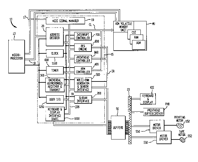
Referring to Fig. 1, a microprocessor control system, generally indicated as
11,
which is preferably intended to control a thermal printing postage meter (not
shown), is comprised of a microprocessor 13 in bus 17 and 18 communication
with
an application specific integrated circuit (ASIC) 15 and a plurality of memory
units
generally indicated as MU. The memory units MU includes non-volatile units
(NVM) and Random Access Memory (RAM). The ASIC 15 is comprised of a number
of integrated circuit modules, for example, ASIC signal manager 19, address
decoder
20, clock 1100, timer module 600, UART module 300, user I/O 1200, keyboard and
display interface 1000, interrupt controller 700, print head controller module
900,
encryption and decryption engine 800, memory controller 400, mufti-PWM
generator
and sensor interface 500 and a slogan interface 200. It should be appreciated
that it is
within the contemplation of the present invention that the IC modules which
make
up the ASIC 15 may vary and the modules here identified are intended to
illustrate
the preferred embodiment of the invention.
The ASIC 15 has an internal data bus (IDB) and a plurality of control lines
CL.
Certain of the modules are in communication with a buffer 50 via an internal
bus
(IR). The buffer 50 is in bus communication with a coupler 23. The coupler 23
is in
communication with various meter devices, such as, the keyboard display drive
KDI,
print head buffer/driver PHB and motor drivers
CA 02152836 2001-07-05
4
550 which drive respective motors 552 the printhead buffer/driver PHB drives a
printer unit PH. In Fig.1, the bus lines IDB and IB, and control lines CL are
depicted
in simplified manner for the purpose of clarity.
Referring to Figs. 1 and 2, the microprocessor 13, in the preferred
embodiment, is a Motorola Module MC68EC000 which passes the control signals
and
data between the microprocessor 13 and the microprocessor interface circuit 19
and
address decoder 20 of the ASIC. The control system address bus is received by
the
ASIC address decoder 20 which generates the necessary control signal on
internal
ASIC control bus CL for enabling the respective modules in accordance with the
address instruction from the microprocessor 13. Low order data from the system
data bus 17 is received by the interface 19 and placed on the internal data
bus to be
placed in the ASIC registers 8 when enabled by the address decoder 20 in
response to
address instructions from the microprocessor. The data placed in the ASIC
registers
8 represents the operating parameters for the respective modules which is
accessed
by the respective modules during when the respective modules have been enabled
by the address decoder 20. A more complete description of the microprocessor
control system is presented in Canadian Patent Application Serial No. 2137495,
entitled "Control System For An Electronic Postage Meter Having A Programmable
Application Specific Integrated Circuit", filed December 7,1994, commonly
assigned.
Referring to Figs. 3 and 4, the print head control module 900 includes a
buffer
903, which in the preferred embodiment is 32 bytes buffer, a shift control
section 913,
a strobe control section 960 and a plurality of registers. The registers are
the control
register 905, status register 907, mode register 909 and strobe register 911.
The strobe
control section 960 is of any suitable conventional configuration and includes
a 8-bit
counter 962 and an N-divider 964. The control section 913 is comprised of a
control
section 930, multiplex section 920, shift section 940 and latch section 950.
Referring also to Fig. 4, in operation, the print controller 900 is provided
with
one of four shift clock values, e.g., 8MHz, 4MHz, 2MHz, lMHz from the timer
module 600. The timer module 600 of any suitable configuration which receives
a
signal clock and suitably divides that signal to produce the desired shift
clock values
as an output. The shift clock values are directed to the muliplexer 920 which
depend
on the state of data bites PMRQ2 and PMRQ3 stored in the mode register 909.
The
selected output from the multiplexer 920 represents the system clock signal
CLOCK.
The system clock signal CLOCK is directed to the print head buffer/ driver PHB
CA 02152836 2001-07-05
and to the clock input of a counter 932 which is part of the control section
930. The
output from the counter 932, which represents the message bit count length of
256
bytes,128 bytes, 64 bytes and 32 bytes, is directed to the input side of a
multiplexer
934. The selection of the appropriate message byte length of the particular
print head
5 buffer/driver PHB is determined by the multiplexer 934 and depends on the
data bit
PMRQO and PMRQ1 of the mode register 909. The output of the multiplexer 934 is
directed to the input of a flip-flop 936 and the rest to the input of a flip-
flop 938. It
should now be appreciated that the output of the flip-flop 938 goes active
when a
data shift is completed to produce a shift complete interrupt which is
directed to the
interrupt controller 700 which informs the microprocessor to indicate a
complete
data transfer. A detailed description of a preferred interrupt controller
system is
described in Canadian Patent Application Serial No. 2137507, filed December
7,1994,
commonly assigned and herein incorporated by reference.
In order to enable data transfer, the output PHCLK from the shift section 940
is driven active in response to the data bit PCRQ(1) in the control register
and, in like
manner, the latch enable signal from the control register 905 is driven active
in
response to the data bit PCRQ(2).
Referring more particularly to Figs. 2 and 3, during system start-up, the
microprocessor 13 addresses the address decoder 20 to enable the writing of
data to
the ASIC registers 8. In particular, data is written to the control register
905, status
register 907, mode register 909 and strobe width register 911. To initiate a
write
cycle, the microprocessor properly addresses the address decoder 20 which
outputs a
control signal PIRB which enables writing of data to the buffer 903. In the
preferred
embodiment, this data represents the necessary data print head driver to cause
printing of a postage indicia by a suitable digital printer. Printing is
commenced by
the microprocessor 13 enabling printing data to be written to the buffer 903
and then
addressing the address decoder to enabling control lines PCRB, PMRB, and SWRB.
As previously noted, the multiplexer 920 responds to provide the selected
shift clock signal to the controller section 930 which then provides the
appropriate
clock signal to the buffer 930 for data transfer to the print head buffer/
driver PHB.
The output from the control register 905 is directed to the shift section 940
to initiate
the actual data transfer from the buffer 903 and to the latch section 950 to
latch enable
the buffer/driver PHB in a conventional manner. The data bit stored in a
strobe
width register determines the value of the N-driver 964 through which a lMHz
signal is
CA 02152836 2001-07-05
6
directed. The output signal is directed to a 8-bit counter 960 through an OR
gate 966.
Also, directed to the OR gate 966 is a control signal from the control
register which
enables the OR gate 966. The strobe signal out put from the strobe section 960
is
directed to buffer/driver PHB. As previously noted, when the data from the
buffer
903 has been transferred, the flip-flop 938 of the control section 960 (refer
to Fig. 4)
issues a shift complete interrupt signal to the microprocessor.
It should now be appreciated that the above printer controller 900 has an
architecture which will allow the printer controller to control both contact
printer
and non-contact printers such as ink jet, laser and thermal transfer. The
printer
controller 900 is suited to provide the printer drivers with the necessary
print data in
a compatible byte size. As a result, an ASIC using a printer controller as
described
has suitable versatility to be employed with a variety of printing
technologies.
The above description represents the preferred embodiment and should not
be viewed as limiting. The scope of the invention is presented in the appendix
claims.