Note : Les descriptions sont présentées dans la langue officielle dans laquelle elles ont été soumises.
2153111
AIR CONDITIONING DEVICE
FIELD OF THE INVENTION
The present invention relates to an air
conditioning device including an inverter circuit that
changes the frequency of a power compressor in an
outdoor device to yield an optimal power for a load,
and more particularly, to an air conditioning device
furnished with an active filter that improves a power
factor and suppresses a higher harmonic current from a
power source.
BACKGROUND OF THE INVENTION
An air conditioner realizing a refrigerating cycle
by sequentially operating a compressor, a condenser, a
decompressor, and an evaporator has been known. A
2~531I1
_ - _ 2 _
recent air conditioner additionally includes an
inverter circuit for supplying an alternating current
driving power to the compressor to control the output
frequency thereof according to a load. This structure
enables the air conditioner to operate at an optimal
power for a load, thereby increasing the
comfortableness of air conditioning while saving
energy.
As shown in Fig. 49, a conventional air
conditioner rectifies an output from a commercial
alternating current power source 501 using a bridge
rectifier circuit 502 composed of four diodes, and
smoothens the rectified voltage using a smoothing
condenser 503 to convert the same into a direct
current, and thus operates as a condenser input type
power supply circuit. The direct current from the
smoothing condenser 503 is converted into an
alternating current of an arbitrary frequency by an
inverter circuit 504 and supplied to a power compressor
505 serving as a load.
The inverter circuit 504 includes a three-phase
transistor bridge circuit composed of six transistors
511- 516 connected to each other through three-phase
bridge connection, and six diodes 521-526 provided in
2153111
- - _ 3
parallel with the transistors 511-516, respectively.
Each of the transistors 511-516 supplies a three-phase
alternating current power to the power compressor 505
when it is turned on at the timing at which a control
signal from an inverter control section 506 is supplied
to the control terminal thereof. The inverter circuit
504 operates most efficiently for a load by controlling
the output frequency according to the load.
In case of the above condenser input type power
supply circuit, an input current flows when an input
voltage is higher than a DC smoothed voltage vo and
stops flowing when the input voltage is lower than Vo
as shown in Fig. 50. As a result, the above condenser
input type power supply circuit presents problems that
more power is lost due to a decrease in the power
factor of the power supply circuit and an increase in a
higher harmonic current, and that the higher harmonic
current adversely affects an AC power line. Also, with
the above-mentioned air conditioner, the power
compressor 505 outputs a large power of 1-2 kW, and the
smoothing condenser 503 correspondingly has a large
capacity, thereby making the above problems more
pronounced.
To eliminate these problems, the IEC
21x3111
- - 4 -
(International Electrotechnical Commission) will impose
a regulation on the higher harmonics current of the
power source in 1996, and some actions must be taken to
comply with the regulation.
Although a structure that employs a passive filter
using a reactor (choke coil) is known as a higher
harmonic current suppressing technique, this structure
is not a perfect countermeasure because it can not
maintain the higher harmonic current under the
regulated value.
Alternately, an air conditioner including an
active filter 507 as shown in Fig. 49 is disclosed in
Japanese Laid-open Patent Application Nos. 4-26374/1992
and 5-68376/1993. To be more precise, the active
filter 507 includes a choke coil 531, a fast recovery
diode 532, and a power transistor 533 between the
bridge rectifier circuit 502 and the smoothing
condenser 503. The switching action of the power
transistor 533 is controlled by a switching control
section 508.
The switching control section 508 controls the
switching action of the power transistor 533 in the
following way.
As shown in Fig. 51, a direct current voltage
213111
- - 5 -
being generated by the smoothing condenser 503 is
detected in resistors 561 and 562 (see Fig. 53) in an
output voltage detecting section 541 in a decompressed
(divided) state. The voltage difference between the
voltage thus detected and a reference voltage generated
by a reference voltage source 542 is outputted from an
error amplifier 543. The reference voltage is set to a
value corresponding to the rated value of the direct
current voltage.
On the other hand, a signal voltage corresponding
to an input voltage to the active filter 507 is
generated by an input voltage detecting section 544
based on an output voltage from the bridge rectifier
circuit 502. Accordingly, a multiplier 545 multiplies
the voltage difference from the error amplifier 543 by
the signal voltage from the input voltage detecting
section 544. As a result, in the multiplier 545, and
the waveform of the input voltage is corrected by the
output from the error amplifier 543. Thus, the output
from the multiplier 545 includes the components
corresponding to both the direct current voltage and
input voltage, and matches with an increase of the
voltage boosted by the active filter 507.
An input current is detected by an input current
CA 02153111 1999-04-27
- 6 -
detecting section 546. The input current thus detected
is amplified in sync with the output of the multiplier
545 by an amplifier 547, thereby making a synchronous
waveform with the input voltage.
The output from the amplifier 547 is compared with
a periodic chopping wave generated by an oscillator 548
by a comparator 549. As shown in Fig. 52, the compara-
for 549 outputs a pulsewise PWM (Pulse Width Modulation)
signal only when the output from the amplifier 547 is
higher than the chopping wave. The PWM signal is ampli-
fied by a driving circuit 550 and supplied to a control
electrode of the power transistor 533. The driving
circuit 550 switches the output of a switching control
signal to on or off by an ON/OFF control signal output-
ted from an output ON/OFF circuit 551 based on a driving
signal.
The active filter 507 is generally known as a
voltage rise chopper type active filter, and it boosts
the output voltage higher than a smoothed voltage
yielded only by the bridge rectifier circuit 502 and
smoothing condenser 503 by exploiting the energy stored
in the choke coil 531. An increase in the boosted
voltage is controlled to be a predetermined rated value
by the switching control section 508.
_ 21531.1
..
The active filter 507 supplies the energy stored
in the choke coil 531 to the smoothing condenser 503
gradually by turning on or off the power transistor 533
at regular frequencies (tens of kilohertz) using the
switching control signal outputted from the switching
control section 508. As a result, the waveform of the
input current is locked with that of the input voltage,
and becomes an approximate sine wave. Thus, the input
power factor is improved while the harmonic distortion
is suppressed, and the utilization efficiency of the
input power is upgraded as a consequence.
In case of the air conditioner such as the one
shown in Fig. 49, it is general to insulate the
inverter control section 506 from the switching control
section 508 and to drive each by their respective power
sources. Thus, signals are sent between the inverter
control section 506 and switching control section 508
through a photo-coupler. Also, the switching control
section 508 has an additional function to detect an
unusual event occurring in the active filter 507, and
upon detecting such an unusual event, it turns on the
photo-coupler by outputting a detection signal to
notify the inverter control section 506 of the unusual
event.
2153111
- - _8_
However, with the above structure, once the
switching control section 508 stops because of an
unusual event, or namely, the power supply to the same
is stopped for. some reason, the switching control
section 508 can not output the detection signal,
thereby making it impossible to notify the inverter
control section 506 of the unusual event. Thus, the
inverter control section 506 can not stop the power
compressor 505, and the power compressor 505 keeps on
operating although the active filter 507 has already
stopped. Moreover, the overcurrent may damage the
devices composing the inverter circuit 504.
It is general to use the above voltage rise
chopper type active filter 507 for an air conditioner
because of its advantages in terms of cost saving and
noise reduction. However, the active filter 507 always
outputs a voltage higher than the input voltage because
of the boosting by the choke coil 531 and power
transistor 533, and the output voltage easily increases
or decreases according to the balance with respect to a
load.
To eliminate this drawbacks, the feedback is
provided by the switching control section 508, so that
the output voltage from the active filter 507 maintains
2153111
_ g _
a constant value. To be more specific, should the
output voltage from the active filter 507 change, the
switching control section 508 controls the switching
action of the power transistor 533 by changing the
pulse width of the PWM signal based on the detected
output voltage from the active filter 507, so that the
output voltage from the active filter 507 will have a
set value demanded by the inverter control section 506.
The output voltage thus detected is also supplied
to the inverter control section 506 as information.
Accordingly, when the output voltage exceeds a certain
range from the set value, the inverter control section
506 judges that either the power compressor 505 has
stopped or something is wrong with the inverter circuit
504, and forcibly stops the active filter 507 to boost
the voltage. Also, an overvoltage protection circuit
which will be described in the next paragraph forcibly
stops the active filter 507 to boost the voltage when
the output voltage exceeds a predetermined protection
voltage.
The overvoltage protection circuit shown in Fig.
53 detects the output voltage from the active filter
507 using a voltage divided by resistors 561~562
provided as voltage dividing circuits of the output
2153111
- - 10 -
voltage detecting section 541, and the detected voltage
is used to judge the overvoltage by a comparator 563.
The comparator 563 compares the detected voltage with a
protection voltage generated by resistors 564.565, and
stops the output action of the driving circuit 550 when
the detected voltage is higher than the protection
voltage.
On the other hand, another overvoltage protection
circuit shown in Fig. 54 uses the output voltage from
the active filter 507 divided by resistors 566.567,
which are different from the resistors 561.562, as the
detected voltage.
However, when the active filter 507 boosts the
output voltage to the set value in activating the
driving action, the output voltage becomes unstable or
exceeds the set value momentarily during a certain
period, such as when the inverter circuit 504 starts or
stops the operation, or the power compressor 505 is
activated or deactivated. The inverter control section
506 judges such a condition as an unusual event even
though the inverter circuit 504, active filter 507,
etc. operate normally, and stops the active filter 507
to boost the voltage, thereby making the operation of
the air conditioner unstable.
2153111
_ -
In particular, when the active filter 507
activates the voltage boosting action, there is a
considerable difference between an initial voltage and
a target voltage of the output voltage, and thus the
gain of the feedback control by the switching control
section 508 becomes greater. Thus, the output voltage
is boosted so rapidly from the start that it overshoots
the target voltage.
Once the active filter 507 has activated the
voltage boosting action, the output voltage from the
active filter 507 drops instantaneously because of the
current flowing through the power compressor 505 at the
time its activation. Correspondingly, the active filter
507 boosts the output voltage using the feedback
control by the switching control section 508 to
compensate such a drop in voltage.
However, once the power compressor 505 has
started, the current flows constantly and hence the
voltage is stabilized. Thus, the boosted output
voltage overshoots the target voltage by an increase
therein. Then, the output voltage drops more than
necessary by the feedback to reduce the overshooted
voltage, and undershoots the target value this time.
The following output voltages remain in a stable
CA 02153111 1999-04-27
- 12 -
condition because the ringing continues with the time
constant of a feedback control system.
Thus, the conventional air conditioner is
disadvantageous in that it stops if the active filter
507 stops when the overvoltage protection circuit
operates on an overshooted output voltage as has been
explained.
The increase value in the overshooted output
voltage is large in an absolute value level, however, it
is generated only in tens of milliseconds. Thus, the
increase of this degree does not exceed the maximum
rated values of the active filter 507, the switching
element of the inverter circuit 504, and the smoothing
condenser 503, and there occurs no problem such as
damaging the elements, limiting the duration of life,
and degrading the performance.
Thus, the operating level of the overcurrent
protection circuit may be raised to prevent the air
conditioner from being stopped by the change in the
input current as a result of the overshoot.
However, by so doing, the overcurrent which should
be detected is not detected, and it becomes impossible
to protect the element from being damaged by the
overcurrent.
213111
- 13 -
Since the protection voltage, which is compared
with the detected voltage by the overvoltage protection
circuit, is yielded by dividing the direct current
voltage by the resistors 564.565, the affect of the
output voltage to the same is negligible. Therefore,
the output voltage and a reference voltage used in the
overvoltage protection circuit are determined
separately. However, variations in the resistor values
of the resistors 561.562 or the resistors 564.565
provided to detect the voltage may reduce the detection
margin (protection voltage minus output voltage) of the
overvoltage protection circuit.
To be more specific, when the resistor values of
the resistor 561 vary in large numbers while those of
the resistors 562 in small numbers, the voltage
dividing circuit detects an output voltage lower than
the normal voltage. Thus, if the output voltage is
controlled based on the value thus detected, the output
voltage is boosted higher than the normal voltage. On
the other hand, when the resistor value of the resistor
564 varies in large numbers while that of the resistor
565 in small numbers, the protection voltage becomes
lower than the normal voltage. Accordingly, the
detection margin lessens, thereby making it easier for
~1~31~11
- 14 -
the overvoltage protection circuit to start the
operation when the output voltage from the active
filter 507 overshoots the normal voltage.
As a result, the overvoltage protection circuit
operates frequently, which presents a problem that the
air conditioner can not operate continuously.
Presently, the detection margin of each air conditioner
is evaluated before the delivery to eliminate this
problem. However, evaluating the detection margin
individually causes problems during the manufacturing
process, such as decreasing yield and making the
inspection troublesome, and makes the resulting air
conditioner expensive.
The conventional air conditioner controls the air
conditioning power by changing the operating frequency
of the power compressor 505 from 15 Hz to 120 Hz.
According to a typical specification, a compressor for
the inverter operates at 60 Hz for the first one minute
from the activation to stabilize the activation and
refrigerating cycle. When the power compressor 505 is
operated under such a specification, the load current
of the same increases because the activation frequency
of 15 Hz increases linearly to the operating frequency
of 60 Hz as shown in Fig. 55.
CA 02153111 1999-04-27
- 15 -
Accordingly, the output voltage from the active
filter 507 decreases as the load current increases.
Then, to compensate such a decrease in the output
voltage, the switching control section 508 boosts the
voltage value under the feedback control, so that the
output voltage is maintained at the constant level.
The above change in the output voltage does not
occur instantaneously as has been explained but it
occurs significantly and continuously over a long time
period. Thus, the feedback control is delayed and
causes a low frequency wave in the output voltage, and
as shown in Fig. 56, the waveform of the input current
to the active filter 507, which is regular in general,
correspondingly shifts to the one having an irregular
fluctuation. As a result, the input current to the
active filter 507 increases over the rated current, and
the overcurrent protection circuit operates to stop the
air conditioner.
To prevent the air conditioner from being stopped
by the change in the input current, the operating level
of the overcurrent protection circuit may be raised.
However, by so doing, the overcurrent caused by an
unusual event which should be detected is not detected,
thereby making it impossible to protect the
21~3~,~11
'' ~ - 16 -
element from being damaged by the overcurrent.
The conventional air conditioner changes the
operating frequency of the power compressor 505 from 10
Hz to 120 Hz (180 Hz in some case) depending on a load
of air-conditioning. However, the ON/OFF action of the
power transistor 533 of the active filter 507 is
controlled independently of the load condition of the
power compressor 505. Thus, the fluctuation of the
output current becomes too large.
As a result, the output voltage from the active
filter 507 decreases under heavy-duty operation, and
the terminal voltage of the smoothing condenser 503, or
namely, the applied voltage to the inverter circuit
504, also decreases. In contrast, the output voltage
from the active filter 507 increases under light-duty
operation, and the applied voltage to the inverter
circuit 504 also increases. Note that, under the
light-duty operation, the voltage applied to the
smoothing condenser 503 and inverter circuit 504 is
above the maximum rated value, thereby possibly causing
damages to the same.
Under the no-load operation, the output voltage
from the active filter 507 increases more than it does
under the light-duty operation. Thus, the smoothing
CA 02153111 1999-04-27
- 17 -
condenser 503 and inverter circuit 504 are more
susceptible to the damages compared with the light-duty
operation.
In addition, the conventional air conditioner has
the following disadvantage in terms of air conditioning
power.
An induction motor is generally used as the
compressor for the inverter, as shown in Fig. 57, the
induction motor has the operating characteristics that
the number of rotations is set to a value at which a
load and a torque are balanced, because the torque is
nil at the synchronous rotational speed No. The
difference between the synchronous number of rotations
and the actual number of rotations is known as slip,
which affects the rotation of the motor significantly.
To be more specific, when the load increases, a
load curve shifts from T1 to T2, and the current in the
motor increases to I1 to I2. Accordingly, the slip also
increases, and the air conditioning power degrades as
the operating frequency, i.e., the number of rotations,
of the power compressor 505 decreases from N1 to N2.
The air conditioning power degrades also when the
current in the motor increases more than the
2.53111
_ 18 _
rated value, because a command value of the operating
frequency of the power compressor 505 is lowered to
reduce the current in the motor.
In the active filter 507, the switching frequency
and switching loss of the power transistor 533,
inductance and ripple current of the choke coil 531,
input current, etc. have close correlation. More
specifically, the ripple current oI in the coil current
is expressed by Equation (1) below.
aI = «/(fsw~L) .....(1)
where « is a constant,
fsw is the switching frequency of the power
transistor 533,
L is the inductance of the choke coil 531.
Hence, given a certain value to the inductance of
the choke coil 531, then multiplying fsw by oI yields a
constant value (fsw x oI = a constant value). Thus, as
shown in Fig. 58, increasing the switching frequency
fsw reduces the ripple current; on the other hand, it
increases the switching loss of the power transistor
533. Therefore, the switching frequency fsw is
generally determined based on the current capacity and
inductance of the choke coil 531.
When the switching frequency fsw is fixed, the
213111
_ _ _ 19 _
number of switching times per period of the power
source output becomes in inversely proportional to the
power source frequency. Thus, there occurs a problem
that the ripple current in the choke coil 531 increases
as the power source frequency becomes lower. For
example, when comparing the case of the power source
frequency of 50 Hz and the power source frequency of 60
Hz, the number of switching per one cycle of the power
source output is greater in the former case than the
latter case. Thus, the former case of the power source
frequency of 50 Hz has a greater ripple current and has
a greater switching loss compared with the latter case
of the power source frequency of 60 Hz. Further, there
occurs a problem that the peak value of the current,
which affects the maximum capacity of the power
transistor 533, increases as the ripple current does
so.
When the direct current level in the coil using a
core is changed, magnetic saturation occurs at a
certain level and the inductance drops abruptly, which
is known as coil's direct current super-imposing
characteristics. In particular, in case of an air
conditioner of a 230-V model, the choke coil 531 used
to boost the voltage has a large maximum coil current
2~~31110_
up to 7 to 8 A rms, and it is almost impossible to make
the direct current super-imposing characteristics flat.
In actual, the inductance of the direct rnrrant
super-imposing characteristics decreases as the coil
current increases as shown in Fig. 59.
It is understood from Equation (1) that the ripple
current increases as the inductance decreases. Thus,
as shown in Fig. 60, the larger the coil current, the
larger the ripple current.
To be more specific, a ripple current oIl is small
when the coil current is small as shown in Fig. 61, and
a ripple current oI2 is fairly large when the coil
current is large as shown in Fig. 62.
The ripple current thus increased can not be
removed by a noise filter and flows through the AC
power supply line, thereby presenting a problem that
the noise level of noise terminal voltage, noise power,
unnecessary radiation, etc. is increased.
The switching control section 508 demands a power
source, such as a power source which outputs a voltage
of +15 V or more, for the amplifier 547 or the like.
Thus, the switching control section 508 is large in
size and fairly expensive.
Further, the switching control section 508
CA 02153111 1999-04-27
- 21 -
controls the switching action in such a manner that the
phase of the input current becomes in sync with that of
the input voltage to approximate to the sine wave.
However, the actual waveform of the input voltage is
distorted because a strain is likely to occur in input
current as it increases, which presents a problem for it
is difficult to approximate the input current to the
sine wave.
The switching control section 508 mainly comprises
a single integrated circuit. Thus, if the integrated
circuit breaks, the output voltage detecting section 541
can not detect an excess increase in the output voltage
when the output value increases more than necessary,
thereby making it impossible to suppress an increase in
the output voltage.
The switching control section 508 finds the
increase in the output voltage by calculating the
voltage balance between the rated value and detected
output voltage, and outputs the PWM signal such that
makes the voltage balance nil. However, there is a
considerable voltage balance at the time of activation
of the active filter 507, and the output voltage changes
after some time has passed since the switching control
signal was outputted to the power transistor
Hz, the number of s
213 x,11
- 22 -
533. Thus, if the switching control signal generated
based on such a considerable voltage balance is
supplied to the power transistor 533 after some time
since the activation of the active filter 507, the
output voltage is boosted higher than the rated value.
Further, when less power is consumed due to the
light-duty operation, the output voltage exceeds the
rated value only by slightly widening the pulse width
of the switching control signal from the switching
control section 508 from a certain pulse width. Thus,
it is required to output the switching control signal
with a narrower range than the certain pulse width. To
meet this requirement, the pulse width of the switching
control signal can vary only in a limited range,
thereby making it difficult to approximate the current
waveform to the voltage waveform. Accordingly, neither
the higher harmonic components in the power supply
current can be suppressed, nor the power factor can be
improved.
Since the voltage balance reaches its maximum at
the activation of the active filter 507, the switching
control signal is outputted with a widened pulse width,
and if the active filter 507 starts up at the crest
value of the input voltage, the current value to be
CA 02153111 1999-04-27
- 23 -
determined by the switching control signal reaches its
maximum pulse width. Since the maximum rated value of
the power transistor 533 is determined by the maximum
current value under such conditions, it is necessary to
secure the maximum rated value for the power transistor
533 even when the maximum current value is far larger
than the current value under the normally controlled
conditions except for the activation. For this reason,
the air conditioner demands a power transistor 533 with
a fairly large maximum rated value, and makes the
resulting air conditioner expensive.
The air conditioner includes a 100V model driven by
a power source voltage of 100V, and a 200V model driven
by a power source voltage of 200V. As shown in Fig. 63,
the former yields a direct current voltage of 280V by
boosting a 100V voltage from the commercial power source
501 through a smoothing coil 561 using a voltage double
rectifier circuit 571 comprising diodes 571a~571b and
condensers 571c ~ 571d. On the other hand, as shown in
Fig.64, the latter yields a direct current voltage by
rectifying a 200V voltage from the commercial power
source 501 using the bridge rectifier circuit 502.
Thus, although it is not shown in the drawing, the
CA 02153111 1999-04-27
- 24 -
air conditioner of the 200V model includes one active
filter 507 like the air conditioner shown in Fig. 49.
However, the air conditioner of the 100V model needs two
active filters 507 for two capacitors 571c and 571d.
Thus, the latter is disadvantageous compared with the
former because it is more expensive.
DESCRIPTION OF THE DRAWINGS
Fig. 1 is a schematic depicting the circuit diagram
of an air conditioner in accordance with the first
embodiment of the present invention.
Fig. 2 is a schematic depicting the circuit diagram
of a circuit for sending a signal between a
microcomputer and a switching control section in the air
conditioner of Fig. 1.
Fig. 3 is a view showing a waveform representing
the operation of an active filter and an inverter
circuit in the air conditioner of Fig. 1.
Fig. 4 is a schematic depicting another circuit
diagram of the air conditioner of Fig. 1 to compensate
an applied voltage to a power compressor when the active
filter breaks down.
Fig. 5(a) is a graph showing the relation between
an operating frequency of the power compressor set
-- 2131115 _
invariably whether the active filter is broken or not
and an effective value of the output from the inverter
circuit.
Fig. 5(b) is a graph showing the relation between
the operating frequency and an applied voltage of the
power compressor when the active filter operates
normally and the same is broken.
Fig. 6(a) is a graph showing the relation between
the operating frequencies of the power compressor set
separately when the active filter operates normally and
the same is broken, and the effective value of the
output from the inverter circuit.
Fig. 6(b) is a graph showing the relation between
the operating frequency and an applied voltage of the
power compressor when the active filter operates
normally and the same is broken.
Fig. 7 is a schematic circuit diagram depicting
the structure of an air conditioner in accordance with
the second embodiment of the present invention.
Fig. 8 is a view showing a waveform representing
the operation of an overvoltage protection circuit at
the activation of the active filter or power compressor
in the air conditioner of Fig. 7.
Fig. 9 is a block diagram depicting the structure
21~3~.11
- 26 -
of a switching control section in the air conditioner
of Fig. 7 when a low-pass filter is provided.
Fig. 10 is a view showing a waveform explaining
how the ringing of the output voltage from the active
filter is deteriorated by the low-pass filter.
Fig. 11 is a schematic circuit diagram depicting
the structure of the switching control section when a
time constant changing section is provided.
Fig. 12 is a view showing a waveform explaining
how the ringing of the output voltage from the active
filter is deteriorated by the time constant changing
section.
Fig. 13 is a schematic circuit diagram depicting
the structure of another overvoltage protection circuit
in the air conditioner of Fig. 7.
Fig. 14 is a graph showing how the operating
frequency of the power compressor is changed by
different changing speed in every predetermined periods
by an inverter control section in the air conditioner
of Fig. 7.
Fig. 15 is a view showing a waveform representing
the an input current to the active filter, which
changes before and after the operating frequency is
changed based on the characteristics shown in Fig. 14.
- 27 -
Fig. 16 is a view showing a waveform representing
the relation between a switching frequency and a ripple
current.
Fig. 17 is a view showing a waveform representing
the relation between a coil current and the switching
frequency.
Fig. 18 is a schematic circuit diagram depicting
the structure to control an oscillating frequency of an
oscillator provided in the switching control section in
accordance with a load current.
Fig. 19 is a graph showing the relation between
the coil current and ripple current indicating that an
increase in the ripple current is suppressed by the
structure shown in Fig. 18.
Fig. 20 is a view showing a waveform of the ripple
current when the coil current is large.
Fig. 21 is a schematic circuit diagram depicting
the structure to boost the output voltage from the
active filter based on the load current and slip of the
power compressor.
Fig. 22 is a view showing the characteristics of
the power compressor improved by the structure of Fig.
21.
Fig. 23 is a schematic circuit diagram depicting
2153111
'L
- 28 -
the structure of an air conditioner in accordance with
the third embodiment of the present invention.
Fig. 24 is a detailed schematic circuit diagram
depicting the structure of a load detecting section in
the air conditioner of Fig. 23.
Fig. 25 is another detailed schematic circuit
diagram depicting the structure of the load detecting
section in the air conditioner of Fig. 23.
Fig. 26(a) is a graph showing the relation between
a load condition of the power compressor and the output
voltage from the active filter.
Fig. 26(b) is graph showing the relation between a
load condition of the power compressor and the output
voltage from the active filter when a set value of the
output voltage from the active filter is changed in
accordance with the load condition of the nnwPr
compressor.
Fig. 27 is a schematic circuit diagram depicting
the structure to change the inductance of a choke coil.
Fig. 28 is another schematic circuit diagram
depicting the structure to change the inductance of the
choke coil.
Fig. 29 is a graph showing the relation between
the load condition of the power compressor and the
2~~3~,11
- - 29 -
output voltage from the active filter when the
inductance of the choke coil is changed by the
structures of Figs. 27 and 28.
Fig. 30 is a schematic circuit diagram depicting a
modified structure of an air conditioner in accordance
with the third embodiment of the present invention.
Fig. 31 is a view explaining a correspondence
between the increased voltage value in the active
filter to be changed and the output voltage (alternate
current voltage) of a commercial power source in case
of the air conditioner of Fig. 30.
Fig. 32 is a schematic circuit diagram depicting
the structure of an air conditioner in accordance with
the fourth embodiment of the present invention.
Fig. 33 is a schematic circuit diagram depicting
the structure of a peak current detecting section in
the air conditioner of Fig. 32.
Fig. 34 is a schematic circuit diagram depicting
the structure of an average current detecting section
in the air conditioner of Fig. 32.
Fig. 35 is a schematic circuit diagram depicting
the structure of an excess voltage rise detecting
section in the air conditioner of Fig. 32.
Fig. 36 is a view showing a waveform representing
2~~3111
- 30 -
a current flowing in the active filter in the air
conditioner of Fig. 32.
Fig. 37 is a schematic circuit diagram depicting
the structure of an air conditioner in accordance with
the fifth embodiment of the present invention.
Fig. 38 is a view showing a waveform representing
the relation between the input voltage and input
current in the air conditioner of Fig. 37.
Fig. 39 is a graph showing the relation between
the input current to the active filter and a switching
frequency when a power source frequency changes in the
air conditioner of Fig. 37.
Fig. 40 is a schematic circuit diagram depicting a
modified structure of an air conditioner in accordance
with the fifth embodiment of the present invention.
Fig. 41 is a schematic circuit diagram depicting
the structure of an air conditioner in accordance with
the sixth embodiment of the present invention.
Fig. 42 is a block diagram depicting the structure
of a major part of another switching control section in
the air conditioner of Fig. 41.
Fig. 43 is a graph showing how the output voltage
from the active filter reaches a target voltage at the
time of activation.
~1~31~~1 _
Fig. 44 is a block diagram depicting the structure
of a major part of another switching control section in
the air conditioner of Fig. 41.
Fig. 45 is a view showing a waveform representing
the relation between the input voltage and a PWM signal
during the operation of the switching control section
of Fig . 44 .
Fig. 46 is a block diagram depicting the structure
of a major part of still another switching control
section in the air conditioner of Fig. 41.
Fig. 47 is a view showing a waveform representing
the relation between the input voltage and the PWM
signal during the operation of the switching control
section of Fig. 46.
Fig. 48 is a schematic circuit diagram depicting
the structure of the air conditioner of Fig. 41 when it
includes another type of active filter.
Fig. 49 is a schematic circuit diagram depicting
the structure of a conventional air conditioner.
Fig. 50 is a view showing a waveform representing
an input voltage and an input current to a condenser
input type power source circuit.
Fig. 51 is a detailed schematic circuit diagram
depicting the structure of a switching control section
213111
- 32 -
in the air conditioner of Fig. 49.
Fig. 52 is a view showing a waveform representing
the operation of a PWM circuit.
Fig. 53 is a schematic circuit diagram depicting
the structure of an overvoltage protection circuit
employed in the conventional air conditioner.
Fig. 54 is a schematic circuit diagram depicting
the structure of another overvoltage protection circuit
employed in the conventional air conditioner.
Fig. 55 is a graph showing how the operating
frequency of a power compressor is changed at a regular
changing speed in the conventional air conditioner.
Fig. 56 is a view showing a waveform representing
an input current to the active filter, which
correspondingly changes before and after the operating
frequency is changed.
Fig. 57 is a view showing the characteristics of a
typical power compressor.
Fig. 58 is a graph showing the relation among a
switching frequency and switching loss of the power
transistor, and a ripple current in the active filter.
Fig. 59 is a graph showing the relation between a
coil current and the inductance of a choke coil.
Fig. 60 is a graph showing the relation between
213111
- 33 -
the coil current and ripple current.
Fig. 61 is a view showing a waveform of the ripple
current when the coil current is small.
Fig. 62 is a view showing a waveform of the ripple
current when the coil current is large.
Fig. 63 is a schematic circuit diagram depicting
the structure of a conventional air conditioner of 100V
model.
Fig. 64 is a schematic circuit diagram depicting
the structure of a conventional air conditioner of 200V
model.
SUMMARY OF THE INVENTION
An object of the present invention is to provide
an air conditioning device which permits a stable
operation, for example, when starting up, and a
protection of components against an abnormality.
Another object of the prevent invention is to provide
an air conditioning device having a simplified
structure by using some components in common.
In order to achieve the above objects, the first
air conditioning device in accordance with the present
invention includes:
rectification means for rectifying an AC voltage
213111
- 34 -
outputted from an AC power source;
smoothing means for smoothing an AC voltage
rectified by the rectification means to be converted
into a DC voltage;
a DC voltage-AC voltage conversion means for
converting by chopping the DC voltage from the
smoothing means into an AC voltage whose variable
voltage and frequency to be applied to a power
compressor;
control means for controlling an output of the DC
voltage-AC voltage conversion means according to a load
state of the power compressor;
an active filter formed between the rectification
means and the smoothing means, for shaping an input
current to be an approximate sine wave almost in phase
with an input voltage;
active filter control means for controlling the
active filter in response to an instruction from the
control means, the active filter control means being
actuated by a power source separately provided from a
power source for the control means; and
abnormality detection means for detecting an
abnormality or a shut-off of at least one of the active
filter and the active filter control means and
213111
- 35 -
detecting a shut-off of a power to be supplied to the
active filter control means as an abnormality.
According to the first air conditioning device,
when an abnormality or a shut off occurs at least in
one of the active filter and the active filter control
means, the occurrence of abnormality or the shut off is
detected by the abnormality detection means. The
abnormality detection means also detects a shut off of
a power to be supplied to the active filter control
means as an abnormality. Since this enables the
control means to detect the shut off of the active
filter control means caused by the stoppage of the
power to be supplied thereto, a necessary operation can
be taken such as stopping the power compressor.
In order to achieve the above objects, the second
air conditioning device in accordance with the present
invention includes:
rectification means for rectifying an AC voltage
outputted from an AC power source;
smoothing means for smoothing an AC voltage
rectified by the rectification means to be converted
into a DC voltage;
a DC voltage-AC voltage conversion means for
converting by chopping the DC voltage from the
213111
- 36 -
smoothing means into an AC voltage whose variable
voltage and frequency vary;
an active filter formed between the rectification
means and the smoothing means, for shaping an input
current to be an approximate sine wave almost in phase
with an input voltage; and
overvoltage preventing means which shuts off the
active filter upon detecting that an output voltage
from the active filter is an overvoltage in excess of a
predetermined threshold, and which does not detect the
overvoltage in excess of the predetermined threshold
for a predetermined time immediately after a turn-on
time and a turn-off time of the DC voltage-AC voltage
conversion means or for a predetermined time
immediately after a turn-on time of the active filter.
According to the second air conditioning device,
the excess output voltage from the active filter will
not be detected by the overvoltage preventing means for
each of the described periods. Therefore, even if an
overshoot occurs in output voltage of the active filter
in the period, the overvoltage preventing means will
not stop the active filter. This enables the second
air conditioning device to be operated under a stable
condition even when the overshoot occurs in output
2153111
_ 37 _
voltage. Under the steady state of the output voltage,
upon detecting the excess output voltage by the
overvoltage preventing means, the active filter is
stopped, thereby preventing an output abnormality of
the active filter.
In order to achieve the above objects, the third
air conditioning device in accordance with the present
invention, include:
rectification means for rectifying an AC voltage
outputted from an AC power source;
smoothing means for smoothing an AC voltage
rectified by the rectification means to be converted
into a DC voltage;
a DC voltage-AC voltage conversion means for
converting by chopping the DC voltage from the
smoothing means into an AC voltage whose voltage and
frequency vary;
an active filter formed between the rectification
means and the smoothing means, for shaping an input
current to be an approximate sine wave almost in phase
with an input voltage; and
overvoltage preventing means which shuts off the
active filter upon detecting that an output voltage
from the active filter is an overvoltage in excess of a
2153111
... . _
- 38 -
predetermined threshold, and which raises the
predetermined threshold for a predetermined time when
starting up the active filter and the power compressor.
According to the third air conditioning device,
the predetermined threshold is raised by the
overvoltage preventing means. Thus, an overshoot does
not occur in the output voltage of the active filter
generated in the described period above the
predetermined threshold, and thus the overvoltage
preventing means will not stop the active filter. This
enables the third air conditioning device to be
operated under a stable condition even when generating
an overshoot of the output voltage. In the stable
condition of the output voltage, upon detecting an
output voltage in excess of a predetermined threshold
of the normal overvoltage by the overvoltage preventing
means, the active filter is stopped, thereby preventing
an occurrence of abnormality in output of the active
filter.
In order to achieve the above objects, the fourth
air conditioning device of the present invention
includes:
rectification means for rectifying an AC voltage
outputted from an AC power source;
213111
= 39 -
smoothing means for smoothing an AC voltage
rectified by the rectification means to be converted
into a DC voltage;
a DC voltage-AC voltage conversion means for
converting by chopping the DC voltage from the
smoothing means into an AC voltage whose voltage and
frequency vary;
an active filter formed between the rectification
means and the smoothing means, for shaping an input
current to be an approximate sine wave almost in phase
with an input voltage;
active filter control means including output
voltage detection means for detecting an output voltage
from the active filter, voltage difference detection
means for outputting a difference between an output
detected by the output voltage detection means and a
reference voltage, and waveform rounding means for
rounding an output from the voltage difference
detection means, the active filter control means
controlling the active filter so as to maintain an
output voltage therefrom constant based on the
difference detected by the voltage difference detection
means; and
overvoltage preventing means which shuts off the
2153111
- 40 -
active filter upon detecting that an output voltage
from the active filter is in excess of a predetermined
threshold.
According to the fourth air conditioning device,
since the waveform of the output from the differential
voltage detection means is shaped to be obtuse by the
waveform obtuse means, the output voltage from the
active filter when starting up the active filter or the
power compressor changes gradually until it reaches the
steady state. Therefore, an occurrence of the
overshoot of the output voltage can be eliminated, and
the overvoltage preventing means will not stop the
active filter. Therefore, even when starting the
active filter or the power compressor, the fourth air
conditioning device can be operated under the stable
condition. Moreover, under the steady state of the
output voltage, as in the case of the third air
conditioning device, an occurrence of abnormality in
output from the active filter can be prevented by the
overvoltage preventing means.
In order to achieve the above objects, the fifth
air conditioning device of the present invention
includes:
rectification means for rectifying an AC voltage
2153111
"' ' - 41 -
outputted from an AC power source;
smoothing means for smoothing an AC voltage
rectified by the rectification means to be converted
into a DC voltage;
a DC voltage-AC voltage conversion means for
converting by chopping the DC voltage from the
smoothing means into an AC voltage whose voltage and
frequency vary;
control means for controlling an output frequency
from the DC voltage-AC voltage conversion means
according to a load state of the power compressor and
lowers a rate of changing speed of an operating
frequency of the power compressor for a predetermined
time immediately after starting an alteration and
immediately before completing the alternation when
altering the operating frequency; and
active filter formed between the rectification
means and the smoothing means, for shaping an input
current to be an approximate sine wave almost in phase
with an input voltage.
According to the fifth air conditioning device,
the operating frequency is altered, for example, when
activating the power compressor, etc., by the control
means at a lower variable speed for a predetermined
_2153111
- 42 -
time immediately after the start of the alteration and
for a predetermined time immediately before the
completion of the alteration. As described, by
providing the period where the variable speed of the
operating frequency is low, large fluctuations of the
input voltage of the active filter can be prevented.
In order to achieve the above object, the sixth
air conditioning device in accordance with the present
invention is arranged so as to include:
rectification means for rectifying an AC voltage
outputted from an AC power source;
smoothing means for smoothing an AC voltage
rectified by the rectification means to be converted
into a DC voltage;
a DC voltage-AC voltage conversion means for
converting by chopping the DC voltage from the
smoothing means into an AC voltage whose voltage and
frequency vary;
an active filter formed between the rectification
means and the smoothing means, for shaping an input
current to be an approximate sine wave almost in phase
with an input voltage;
a load detection means for detecting a load state
of the power compressor;
_2153111
- 43 -
output voltage setting means for setting an output
voltage from the active filter according to the load
state of the power compressor; and
active filter control means for controlling the
active filter based on a predetermined output voltage.
According to the sixth air conditioning device,
upon detecting the load state of the power compressor
by the load state detection means, the output voltage
to be applied to the active filter control means is set
by the output voltage setting means according to a
detection value of the load state detection means.
Then, the active filter control means controls the
active filter based on the set value.
Therefore, even if the output voltage from the
active filter drops due to an increase in load of the
power compressor, by increasing the output voltage
according to the load by the active filter control
means, a drop in output voltage can be prevented. On
the other hand, when the load of the power compressor
becomes lighter, by lowering the output voltage by the
active filter control means according to the load, a
rise in output voltage can be prevented. Therefore,
the described arrangement enables the output voltage to
be maintained constant irrespectively of variations in
_21~31I1
.,._ _ 4 4 _
load.
In order to achieve the above object, the seventh
air conditioning device in accordance with the prevent
invention includes:
rectification means for rectifying an AC voltage
outputted from an AC power source;
smoothing means for smoothing an AC voltage
rectified by the rectification means to be converted
into a DC voltage;
a DC voltage-AC voltage conversion means for
converting by chopping the DC voltage from the
smoothing means into an AC voltage whose voltage and
frequency vary to be applied to the power compressor;
an active filter formed between the rectification
means and the smoothing means, for shaping an input
current to be an approximate sine wave almost in phase
with an input voltage, a ground potential thereof
matching that of the DC voltage-altering voltage
conversion means;
active filter control means for controlling the
active filter; and
power supply means for supplying a driving power
to the DC voltage-AC voltage conversion means through a
power supply output terminal, the power supply means
2153111
- 45 -
supplying a driving power also to the active filter
control means through another power source output
terminal.
According to the seventh air conditioning device,
in the power source means, the ground potential of the
DC voltage-AC voltage conversion means and the ground
potential of the active filter are identical, the power
source for the active filter control means and the
power source for the DC voltage-AC voltage conversion
means are used in common. As the power source means
has a separately provided power source output,
respective power sources for use exclusive use in the
active filter control means and the DC-AC conversion
means are not needed.
In order to achieve the above object, the eighth
air conditioning device in accordance with the present
invention includes:
rectification means for rectifying an AC voltage
outputted from an AC power source;
smoothing means for smoothing an AC voltage
rectified by the rectification means to be converted
into a DC voltage;
a DC voltage-AC voltage conversion means for
converting by chopping the DC voltage from the
215436111
smoothing means into an AC voltage whose voltage and
frequency vary to be applied to the power compressor;
an active filter formed between the rectification
means and the smoothing means, the active filter
including a choke coil, the active filter shaping an
input current to be an approximate sine wave almost in
phase with an input voltage by adjusting a flow of
current into the smoothing means through the choke coil
by switching a switching element; and
switching control means for varying a switching
frequency of the switching element according to at
least one of a current flowing through the choke coil
and an output frequency of the AC power source.
According to the eighth air conditioning device,
for example, when a switching frequency is raised
according to an increase in current flowing through the
choke coil by the control of the switching control
means, even if the inductance of the choke coil is
lowered due to the direct current superimposing
characteristic, an increase in ripple current can be
prevented. This is true also in the case of raising
the switching frequency when the output frequency of
the alternating source is raised.
In order to achieve the above objects, the ninth
21x3111
- 47 -
air conditioning device in accordance with the present
invention includes:
rectification means for rectifying an AC voltage
outputted from an AC power source;
smoothing means for smoothing an AC voltage
rectified by the rectification means to be converted
into a DC voltage;
a DC voltage-AC voltage conversion means for
converting by chopping the DC voltage from the
smoothing means into an AC voltage whose voltage and
frequency vary to be applied to the power compressor;
an active filter formed between the rectification
means and the smoothing means, for shaping an input
current to be an approximate sine wave almost in phase
with an input voltage;
active filter control means for controlling the
active filter;
overvoltage detection means for detecting that an
output voltage from the active filter is an overvoltage
of not less than a predetermined voltage; and
power supply stop means for stopping a power to be
supplied to the active filter control means when the
output voltage from the active filter is an
overvoltage.
CA 02153111 1999-04-27
- 48 -
According to the ninth air conditioning device,
upon detecting an excess output voltage from the active
filter by the overvoltage detection means, the power
supply to the active filter control means is stopped by
the power supply stop means. Then, the active filter
control means stops the control of the active filter by
stopping the power to be supplied thereto. As a result,
the active filter can be surely prevented from
overheating even if an overheat of the output voltage
occurs by any cause.
In order to achieve the above objects, the tenth
air conditioning device in accordance with the present
invention includes:
rectification means for rectifying an AC voltage
outputted from an AC power source;
smoothing means for smoothing an AC voltage
rectified by the rectification means to be converted
into a DC voltage;
a DC voltage-AC voltage conversion means for
converting by chopping the DC voltage from the smoothing
means into an AC voltage whose voltage and frequency
vary to be applied to a power compressor;
an active filter formed between the rectification
means and the smoothing means, for shaping an input
21311 1
current to be an approximate sine wave almost in phase
with an input voltage;
output voltage detection means for detecting an
output voltage from the active filter;
error detection means for detecting a difference
between an output voltage and a reference voltage set
beforehand;
output control means for controlling an output
voltage from the active filter to be maintained
constant based on the difference; and
limiting means for limiting the difference between
the output voltage and the reference voltage to be not
more than a predetermined value when starting up the
active filter.
According to the tenth air conditioning device, a
difference between the output voltage detected by the
output voltage detection means and the reference
voltage is detected by the error detection means.
Then, the output voltage from the active filter is
maintained constant under the control of the output
control means. On the other hand, when starting up the
active filter, the control means limits the difference
to be not more than a predetermined value. As a
result, since the difference between the output voltage
2153111
-- . - - 50 -
and a reference voltage becomes smaller than the actual
value, an excess rise in output voltage due to a great
difference between the output voltage at turn-on time
and the target voltage of the output voltage can be
prevented.
In order to achieve the above objects, the
eleventh air conditioning device in accordance with the
present invention includes:
rectification means for rectifying an AC voltage
outputted from an AC power source;
smoothing means for smoothing an AC voltage
rectified by the rectification means to be converted
into a DC voltage;
a DC voltage-AC voltage conversion means for
converting by chopping the DC voltage from the
smoothing means into an AC voltage whose voltage and
frequency vary to be applied to a power compressor;
an active filter formed between the rectification
means and the smoothing means, the active filter
shaping an input voltage to be an approximate sine wave
almost in phase with an input voltage by adjusting a
flow of current into the smoothing means by switching a
switching element;
zero cross detection means for detecting a zero
213111
-51-
cross point of the input voltage of the active filter;
and
activation means for starting up the active filter
at a zero cross point of the input voltage.
According to the eleventh air conditioning device,
upon detecting a zero cross point of the input voltage
by the zero cross detection means, the active filter is
activated by the activation means at the zero cross
point. Since the amplitude of the input voltage
becomes zero at a zero cross point, the switching width
of the switching element is minimized. Therefore, when
starting up the active filter at which the difference
between the actual output voltage and the target
voltage is maximized, the current flowing through the
switching element becomes small, and the maximum
current of the switching element can be made smaller.
Therefore, the maximum rate of the switching element
can be reduced, and the reduction in cost of the
switching element and an improved reliability can be
achieved.
In order to achieve the above object, the twelfth
air conditioning device in accordance with the present
invention includes:
rectification means for rectifying an AC voltage
215111
- 52 -
outputted from an AC power source;
smoothing means for smoothing an AC voltage
rectified by the rectification means to be converted
into a DC voltage;
a DC voltage-AC voltage conversion means for
converting by chopping the DC voltage from the
smoothing means into an AC voltage whose voltage and
frequency vary to be applied to a power compressor;
an active filter formed between the rectification
means and the smoothing means, the active filter
including a choke coil and shaping an input current to
be an approximate sine wave almost in phase with an
input voltage by adjusting a flow of current into the
smoothing means through the choke coil by switching a
switching element; and
inductance alternation means for increasing an
inductance of the choke coil for a predetermined time
after starting up the active filter.
According to the twelfth air conditioning device,
since the inductance of the choke coil increases for a
predetermined time after starting up the active filter
by the inductance alteration means, the current flowing
through the choke coil for the period becomes smaller.
Therefore, when activating the active filter, the
213111
- 53 -
current flowing through the switching element becomes
smaller, thereby enabling a smaller maximum current of
the switching element. Therefore, a reduction in cost
of the switching element and an improved reliability
can be achieved as in the case of the eleventh air
conditioning device.
In order to achieve the above object, the
thirteenth air conditioning device in accordance with
the present invention include:
rectification means for rectifying an AC voltage
outputted from an AC power source;
smoothing means for smoothing an AC voltage
rectified by the rectification means to be converted
into a DC voltage;
a DC voltage-AC voltage conversion means for
converting by chopping the DC voltage from the
smoothing means into an AC voltage whose voltage and
frequency vary to be applied to a power compressor;
an active filter formed between the rectification
means and the smoothing means, for shaping an input
current to be an approximate sine wave almost in phase
with an input voltage;
an AC voltage detection means for detecting an AC
voltage of the AC power source;
CA 02153111 1999-04-27
- 54 -
voltage rise setting means for setting a voltage
rise value for an output from the active filter
according to the AC voltage of the AC power source; and
active filter control means for controlling the
output voltage from the active filter based on a
predetermined voltage rise value.
According to the thirteenth air conditioning
device, upon detecting an AC voltage by the AC voltage
detection means, a voltage rise value for the output
voltage is set according to the AC voltage detected by
the voltage rise setting means. Here, the voltage rise
value is set such that, for example, the voltage rise
value for the 100 V air conditioning device is twice as
much as that of the 200 V air conditioning device. In
this way, the active filter is controlled by the active
filter control means based on the set value.
The described arrangement enables the output
voltage from the active filter to be maintained constant
irrespective of the AC voltage. Therefore, among
different kinds of the AC voltage, the active filter can
be used in common, thereby reducing the number of
components.
In order to achieve the above object, the
fourteenth air conditioning device in accordance with
213111
- 55 -
the present invention includes:
rectification means for rectifying an AC voltage
outputted from an AC power source;
smoothing means for smoothing an AC voltage
rectified by the rectification means to be converted
into a DC voltage;
a DC voltage-AC voltage conversion means for
converting by chopping the DC voltage from the
smoothing means into an AC voltage whose voltage and
frequency vary to be applied to a power compressor;
an active filter formed between the rectification
means and the smoothing means, the active filter
shaping an input current to be an approximate sine wave
almost in phase with an input voltage by adjusting a
flow of current into the smoothing means by switching a
switching element;
input voltage detection means for detecting an
input voltage to the active filter;
waveform generation means for generating a sine
wave like waveform according to a phase angle of the
input current of the active filter; and
phase synchronization means for synchronizing the
sine wave like waveform with a phase of the input
voltage of the active filter; and
CA 02153111 1999-04-27
- 56 -
switching control means for controlling a switching
of the switching element based on the sine wave like
waveform in synchronous with the input voltage.
According to the fourteenth air conditioning
device, the sine wave like waveform generated from the
wave generation means is used in place of the waveform
of the actual input current. The sine wave like
waveform is made in phase with the input voltage. Then,
the switching of the switching element is controlled by
the switching control means based on the sine wave like
waveform in phase with the input voltage by the
switching control means.
Therefore, even when a large distortion of the
input current occurs, by adopting the sine wave like
waveform, the switching can be controlled to achieve the
target value being affected. In general, the described
sine wave like waveform is generated in a digital form
by the calculation by the computer, etc. As a result,
an improved noise resistance of the waveform can be
achieved, thereby enabling a stable switching control.
For a fuller understanding of the nature and
advantages of the invention, reference should be made
213111
-.... _ 5 7 _
to the ensuing detailed description taken in
conjunction with the accompanying drawings.
DESCRIPTION OF THE EMBODIMENTS
[FIRST EMBODIMENT]
The following descriptions will discuss one
embodiment of the present invention in reference to
Fig. 1 through Fig. 3.
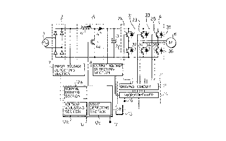
As shown in Fig. 1, an air conditioning device in
accordance with the present embodiment includes a
bridge rectifying circuit 2, a smoothing condenser 3,
an inverter circuit 4 and an active filter 5 as a power
source system. The air conditioning device also
includes an input voltage detecting section 7, an
output voltage detecting section 8, an inverter control
section 11, a switching control section 12 and an
interface section 13 (I/F in figures) as a control
system. The inverter control section 11 is composed of
a microcomputer 14 and a driving circuit 15.
The power source system is provided for generating
a DC voltage by rectifying an output from a commercial
power source 1 in a bridge rectifying circuit 2 and
smoothing it by the smoothing condenser 3. Further,
based on the DC voltage , an AC voltage of three phases
2153111
- ~ - - 5s -
is generated by the inverter circuit 4 to be applied to
a power compressor 6.
The inverter circuit 4 includes six transistors 21
through 26 and six diodes 31 through 36. The
transistors 21 and 22, the transistors 23 and 24 and
the transistors 25 and 26 are respectively connected in
series between two AC power source lines. On the other
hand, the diodes 31 through 36 are respectively
connected to the transistors 21 through 26 in parallel.
The inverter circuit 4 outputs an AC voltage of three
phases by switching the transistors 21 through 26 under
the control of the microcomputer 14.
The power compressor 6 is connected to respective
junctions between the transistors 21 and 22, the
transistors 23 and 24 and the transistors 25 and 26.
The power compressor 6 is actuated by the AC voltage of
three phases from the inverter circuit 4.
In the power source system, the active filter 5 is
connected between the bridge rectifying circuit 2 and
the smoothing condenser 3. The active filter 5
includes a choke coil 41, a fast recovery diode 42 and
a power transistor 43. In the present embodiment, an
insulating gate bipolar transistor is adopted as the
power transistor 43. However, other high speed
215311
_ 59 _
switching element may be used.
The choke coil 41 and the fast recovery diode 42
are provided in series on the positive electrode side
of the power source line. The power transistor 43
(switching element) is arranged such that a collector
thereof is connected to a junction of one end of the
choke coil 41 and an anode of a fast recovery diode 42,
and an emitter thereof is connected to the power source
line on the negative electrode side.
The active filter 5 is provided for improving a
harmonic suppression and a power factor. The active
filter 5 controls a current flowing through the choke
coil 41 with respect to the current flowing into the
smoothing condenser 3 through the choke coil 41 and the
fast recovery diode 42 by switching the power
transistor 43.
In the control system, the microcomputer 14
controls switching of the transistors 21 through 26
according to an air conditioning load so as to control
an output frequency of the inverter circuit 4. The
microcomputer 14 activates the switching circuit 12 in
synchronous with a starting time of the power
compressor 6.
On the other hand, the switching control section
213111
- 60 -
12 controls an output voltage from the active filter 5
by controlling the pulse width of the switching control
signal to be applied to a control electrode of the
power transistor 43. The switching control section 12
performs a feedback control so as to maintain the
output voltage from the active filter 5 constant.
The input voltage detecting section 7 includes a
voltage dividing circuit composed of, for example, a
resistor. The input voltage detecting section 7
divides and detects an input voltage to the active
filter 5 generated between the rectifying power source
lines. The output voltage detecting section 8 also
includes the same voltage dividing circuit. The output
voltage detecting section 8 divides and detects an
output voltage from the active filter 5 generated
between the DC power source lines.
The switching control section 12 includes a normal
driving section 12a, a voltage adjusting section 12b
and a state detecting section 12c.
Based on the control signal from the microcomputer
14 (to be described later), the normal driving section
12a generates a switching control signal based on the
input voltage detected by the input voltage detecting
section 7. More specifically, the normal driving
213111
- 61 -
section 12a controls the ON/OFF of the power transistor
43 so as to adjust the current flowing into the
smoothing condenser 3 from the choke coil 41 through
the fast recovery diode 42 in synchronous with the
input voltage waveform from the bridge rectifying
circuit 2. By the operation of the normal driving
section 12a, the input current waveform is shaped to be
an approximate sine wave.
The voltage adjusting section 12b controls an
output voltage by varying the time duration of the
ON/OFF of the power transistor 43 according to a change
in output voltage detected by the output voltage
detecting section 8. The output voltage of the active
filter 5 is adjusted to the voltage value set by the
microcomputer 14.
The state detecting section 12c detects if an
abnormality has occurred in the active filter 5 based
on the output voltage detected by the output voltage
detecting section 8. More specifically, the state
detecting section 12c outputs an abnormality detecting
signal when the detection voltage from the output
voltage detecting section 8 is set below a
predetermined level so as to detect the active filter 5
in the abnormal state or the stop state.
. 213111
- - 62 -
The microcomputer 14 controls each section of the
air conditioner based on the content set by the
operating section (not shown) provided in a main body
of the air conditioner of the present embodiment. The
microcomputer 14 outputs a drive control signal to the
driving circuit 15 based on the output voltage detected
by the output voltage detecting section 8. The driving
circuit 15 generates a drive signal to be applied to a
base of the transistors 21 through 26 at a timing based
on the control signal.
The microcomputer 14 stops the inverter circuit 4
upon detecting the occurrence of abnormality in the
active filter 5 by the state detecting section 12c.
Further, the microcomputer 14 determines that the power
compressor 6 is in the stop state or an abnormality has
occurred in the inverter circuit 4 when a detected
voltage by the output voltage detecting section 8
exceeds a predetermined value, and is further raised
above a predetermined voltage value and stops the
active filter 5.
A circuit for connecting the microcomputer 14 and
the switching control section 12 will be explained.
The microcomputer 14 and the switching control
section 12 are electrically insulated, and are driven
213111
. . _
- 63 -
independently respectively by the power sources 16 and
17. A communication of the signal is performed
optically through the interface section 13 between the
microcomputer 14 and the switching control section 12.
As shown in Fig. 2, the interface section 13 is
composed of the photocouplers 13a and 13b. The
photocoupler 13a is composed of a light emitting diode
18 and a photo transistor 19. The photocoupler 13b is
composed of a light emitting diode 45 and a photo
transistor 46. The photocoupler 13a and the state
detecting section 21c constitute abnormality detection
means.
The light emitting diode 18 is arranged such that
an anode thereof is connected to the power source 17,
and a cathode thereof is connected to the state
detecting section 12c. The photo transistor 19 is
arranged such that the collector is connected to an
abnormality detection port (hereinafter simply referred
to as a port ) S of the microcomputer 14 and the power
source 16.
The light emitting diode 45 is arranged such that
an anode thereof is connected to the power source 16
and a cathode thereof is connected to the control
signal output port (hereinafter simply referred to as a
-- ~ _ 215 311s
port) T of the microcomputer 14 through the transistor
47. The photo transistor 46 is arranged such that the
collector is connected to the power source 17 and to
the normal driving section 12a through the transistor
48.
In the state where the switching control section
12 is normally operated by the power supplied from the
power source 17, the photocoupler 13a is set in the ON
position in the described circuit. As a result, a low
level signal is always inputted to the port S in the
microcomputer 14.
In response to the low level signal inputted to
the port S, the microcomputer 14 determines that the
active filter 5 and the switching control section 12
are in the normal state, and transmits a high level ON
signal from the port T. In response to the ON signal,
the photocoupler 13b is set in its ON position, and the
power is supplied to the normal driving section 12a
from the power source 17. As a result, the normal
driving section 12a is set in the operable state.
On the other hand, if an abnormality has occurred
which cause the power supply to the switching control
section 12 to stop, the photocoupler 13a is set in its
OFF position. As a result, the high level signal is
- 21~31~~
inputted to the port S of the microcomputer 14. Even
when the switching control section 12 is in the normal
state, if an abnormality in the active filter 5 is
detected by the state detecting section 12c, the
photocoupler 13a is set in the OFF position, and a high
level signal is inputted to the port S.
In response to the signal of the high level
inputted to the port S, the microcomputer 14 determines
that an abnormality has occurred in at least one of the
active filter 5 and the switching control section 12,
and transmits a low level OFF signal from the port T.
Then, the photocoupler 13b is turned OFF by an OFF
signal, and a power is not supplied to the normal
driving section 12a from the power source 17. As a
result, the normal driving section 12a is set in an
inoperable state.
According to the air conditioner in accordance
with the present invention, upon pressing a start
button of the operational unit, a high level ON signal
is transmitted from the port T of the microcomputer 14
so as to set the photocoupler 13b in the ON position.
Then, the power is supplied to the switching control
section 12. As a result, as shown in Fig. 3, the
active filter 5 starts driving, and after an elapse of
2153111
- - 66 -
a predetermined time, the inverter circuit 4 also
starts driving.
In the power source system, the AC voltage from
the commercial power source 1 is full wave rectified by
the bridge rectifying circuit 2, and then inputted to
the active filter 5. The switching control section 12
switches ON/OFF the power transistor 43 according to a
control signal from the microcomputer 14 so that the
output voltage from the active filter 5 becomes the set
value.
Since the power transistor 43 is set in the OFF
position when the current flowing through the choke
coil 41 is set to a predetermined value, the power is
stored in the choke coil 41. On the other hand, since
the power transistor 43 is turned ON when the current
flowing through the collector and the emitter becomes
higher than a predetermined value, the power stored in
the choke coil 41 is released.
As a result, the input current waveform becomes a
sine wave in phase with the input voltage waveform, and
the output voltage from the active filter 5 is raised
to a predetermined value. The raised output voltage is
smoothened by the smoothing condenser 3, and then
supplied to the inverter circuit 4. As a result, the
_ 21~3~.11
- 67 -
generation of the harmonic current can be suppressed,
and the power factor can be improved, thereby achieving
an effective use of the power source.
On the other hand, when the inverter circuit 4
starts driving, a drive control signal is outputted
from the microcomputer 14 to the driving circuit 15.
Then, the driving circuit I5 switches the six
transistors 21 through 26. As a result, the output
voltage from the active filter 5 is chopped. The power
compressor 6 is driven with an application of the
chopped voltage (PWM waveform). By driving the power
compressor 6 in the described manner, the air
conditioner of the present invention starts driving.
During the operation of the air conditioner in
accordance with the present invention, the switching
control section 12 always detects an output voltage
from the active filter 5 by the output voltage
detecting section 8. The switching control section 12
adjusts the output voltage by varying the time duration
of the ON/OFF of the power transistor 43 according to
the change in the output voltage.
The photocoupler 13a is always set in the ON
position by the state detecting section 12c, and thus a
low level signal is inputted to the port S of the
213111
- 68 -
microcomputer 14. Then, from the low level signal, the
microcomputer 14 determines that the active filter 5 or
the switching control section 12 is in the normal
state, and continues the normal operation of the air
conditioner of the present embodiment.
By stopping the supply of the power, for example,
when an abnormality occurs in the active filter 5 or
the switching control section 12, the photocouplers 13a
and 13b are turned OFF in the interface section 13.
Thus, the active filter 5 is stopped driving, and the
application voltage to the power compressor 6 becomes
short, thereby presenting the problem that the power
compressor 6 is easily locked, or may even stop
operating.
In order to counteract the above-mentioned
problem, the photocoupler 13a is set in the OFF
position, so that the signal of the high level is
inputted to the port S. In response to the input
signal, the microcomputer 14 determines that an
abnormality has occurred in the active filter 5 or the
switching control section 12, and stops the operation
of the inverter circuit 4 immediately.
The shortage of the application voltage to the
power compressor 6 due to the abnormality occurred in
213111
- 69 -
the active filter 5 can be prevented by other
arrangements (to be described later).
Furthermore, the microcomputer 14 always detects
the output voltage from the active filter 5 by the
output voltage detecting section 8. For example, when
the operation of the power compressor 6 is stopped, or
the abnormality has occurred in the inverter circuit 4,
the output voltage would exceed the set value and is
further raised above an overvoltage detection value
(shown in Fig. 3). Then, a low level OFF signal is
sent from the port T of the microcomputer 14. In
response to the low level OFF signal, the photocoupler
13b is set in the OFF position. When the photocoupler
13b is set in the OFF position, as the power supply to
the normal driving section 12a is stopped, the active
filter 5 would be stopped operating.
Additionally, when the active filter 5 or the
inverter circuit 4 is stopped due to the abnormality
occurred therein, the user would be informed by an LED,
buzzer, etc., formed on the indoor unit of the air
conditioner of the present embodiment. In the case
where the air conditioner of the present embodiment is
stopped by pressing the stop button in the operational
unit, or by automatically stopping the air conditioner
- 21531~~ _
by the timer, the inverter circuit 4 also stops
driving. After a predetermined time has elapsed after
stopping the inverter circuit, the active filter 5 is
also stopped driving, thereby terminating the operation
of the air conditioner.
As described, a signal is transmitted and received
between the microcomputer 14 and the switching control
section 12 through the interface section 13 composed of
the photocouplers 13a and 13b. Therefore, when an
abnormality has occurred in the active filter 5 or the
switching control section 12, a signal of the high
level is inputted to the port S so as to inform the
microcomputer 14 of the occurrence of the abnormality.
As a result, the active filter 5 can be prevented from
being driven by the microcomputer 14 even when the
abnormality has occurred.
The microcomputer 14 stops the inverter circuit 4
upon detecting the abnormal state or the stop state of
the active filter 5 or the switching control section
12. As a result, the power compressor 6 can be
prevented from being locked due to the shortage of the
application voltage.
Furthermore, when the output voltage from the
active filter 5 is raised above the overvoltage
21531.1
- 71 -
detection value, the microcomputer 14 determines that
the inverter circuit 4 is in the abnormal state or the
stop state and stops the operation of the active filter
5. As a result, the smoothing condenser 3 and the
inverter circuit 4 can be prevented from breaking due
to the overvoltage, and the occurrence of the secondary
fault can be prevented.
When the active filter 5 starts driving, the
output voltage is raised with respect to the input
voltage. Here, in response to the time lag of the
feedback through the output voltage detecting section
8, as shown in Fig. 3, the output voltage may be raised
above the overvoltage detection value for an instant.
Furthermore, since a steady output voltage cannot be
achieved also when the inverter circuit 4 starts and
stops driving, the overvoltage may be generated as in
the aforementioned case. In this case, although each
section is being driven in a normal condition, the
microcomputer 14 determines it to be in the abnormal
condition by the overvoltage protecting function and
stops the active filter 5.
As shown in Fig. 3, in the microcomputer 14, an
abnormality detection inhibiting period t, in which the
detection of the abnormality is not performed, is set
CA 02153111 1999-04-27
- 72 -
immediately after starting and stopping the driving of
the inverter circuit 14 or immediately after starting
the driving of the active filter 5. Therefore, even if
the high level signal is inputted to the port S in the
abnormality detection inhibiting period t, neither the
active filter 5 nor the inverter circuit 4 would be
stopped. As a result, the problem that the active
filter 5 and the inverter circuit 4 are stopped in the
normal operation can be prevented, thereby driving the
air conditioner of the present invention in a stable
condition.
In the present embodiment, the state detecting
section 12c is formed in the switching control section
12. However, the present invention is not limited to
this, and the state detecting section 12c may be
actuated by a separately provided power source from the
microcomputer 14 or the switching control section 12.
Alternatively, it may be also arranged such that the
microcomputer 14 also serves as the state detecting
section 12c for directly detecting the state of the
active filter 5 or the switching control section 12.
Another arrangement for preventing the shortage of
the power of the power compressor 6 will be explained.
As shown in Fig. 4, the described arrangement
2153111
- 73 -
includes a fault detecting section 51 for detecting the
fault of the active filter 5 and the pattern change
section 52.
The fault detecting section 51 may be the circuit
for detecting the fault of the active filter 5, for
example, by detecting the load state of the power
compressor 6. The fault detecting section 51 may be an
output voltage detecting section 8 or the circuit for
detecting the load current. When using the output
voltage detecting section 8 as the fault detecting
section 51, the stoppage of the power compressor 6 is
detected by a drop in output voltage.
The pattern change section 52 changes the table of
the V/F pattern which represent the correlation between
the driving signal voltage to be applied to the
inverter circuit 4 from the inverter control section 11
and the operating frequency.
Normally, the correlation between the effective
value of the output voltage from the inverter circuit 4
and the operating frequency is on the assumption that
the active filter 5 is being operated. Therefore, as
shown in Fig. 5(a), the correlation is determined by
the V/F pattern. However, when the active filter S is
in failure, since the voltage rising operation by the
_213111
- 74 -
active filter 5 cannot be performed, as shown in Fig.
5(b), the voltage to be actually applied to the power
compressor 6 would drop.
On the other hand, in the event of a failure in
the active filter 5, the pattern change section 52
changes the V/F pattern (the linear line representing
the off position of the active filter) as shown in Fig.
6(a). As a result, when a failure occurs in the active
filter 5, the output voltage of the active filter 5
becomes higher than the normal operation state, and the
effective value of the output voltage from the inverter
circuit 4 with respect to the operating frequency of
the power compressor 6 becomes higher than the normal
operation state of the active filter 5.
As a result, the correlation between the voltage
to be actually applied to the power compressor 6 and
the operating frequency is maintained constant
irrespectively of the state of the active filter 5
(normal or abnormal) as shown in Fig. 6(b). Therefore,
even if a failure occurs in the active filter 5, the
operation of the air conditioner can be continued
without stopping the power compressor 6.
However, in the described state, since the
operation is continued, it is required to inform the
213111
- 75 -
user of the failure of the active filter 5. As
previously mentioned, the LED, the buzzer, etc., is
used for informing the user that it is not in the
normal operational mode. Since this enables the
operation of the air conditioner to be continued as an
emergency operation until the serviceman arrives, the
user can manage the failure more efficiently.
[SECOND EMBODIMENT
The following description will discuss the second
embodiment of the present invention in reference to
Fig. 7 through Fig. 22. For convenience in
explanations, members having the same functions as the
first embodiment will be designated by the same
reference numerals, and thus the description thereof
shall be omitted here.
As shown in Fig. 7, an air conditioner in
accordance with the present embodiment is provided with
the switching control section 60. The switching
control section 60 is provided for controlling the
output voltage from the active filter 5 by controlling
a pulse width of a switching control signal to be
applied to a control electrode of the power transistor
43. The switching control section 60 performs a
CA 02153111 1999-04-27
- 76 -
feedback control so as to maintain an output voltage
from the active filter 5 constant.
The switching control section 60 includes an input
voltage detecting section 61, an output voltage
detecting section 62, a reference power source 63, an
error amplifier 64, an input current detecting section
65, a multiplier 66, an amplifier 67, an oscillator 68,
a comparator 69 and a driving circuit 70. The switching
control section 60 includes resistors 71 through 73, a
comparator 74 and a switch 75 as an overvoltage
protection circuit.
Other than the resistors 71 through 73, the
comparator 74 and the switch 75, the overvoltage
protecting circuit includes resistors 76 and 77. The
resistors 76 and 77 are formed between the active filter
and the smoothing condenser 3 in the power source
system, for dividing and detecting the output voltage
from the active filter 5.
A main control section composed of the input
voltage detecting section 61, the output voltage
detecting section 62, the reference power source 63, an
error amplifier 64, the input current detecting section
65, the multiplier 66, the amplifier 67, the oscillator
68, the comparator 69 and the driving
CA 02153111 1999-04-27
_ 77 _
circuit 70 has almost the same function as the switching
control section in the aforementioned conventional air
conditioner (see Fig. 50).
Namely, in the main control section, the DC voltage
generated in the smoothing condenser 3 is detected by
the output voltage detecting section 62, and the voltage
difference between the detected value and the reference
voltage generated from the reference power source 63 is
outputted from the error amplifier 64. In the
multiplier 66, the difference voltage from the error
amplifier 64 is multiplied by the voltage waveform from
the input voltage detecting section 61, while the
current to be inputted to the active filter 5 is fetched
from the emitter side of the power transistor 43 , and
the signal voltage according to the current value is
detected by the input current detecting section 65.
In the amplifier 67, the difference between the
detection value and the output from the multiplier 66 is
amplified. The output from the amplifier 67 is
converted to a PWM signal by the PWM circuit composed of
the comparator 69 and the oscillator 68. The PWM signal
is amplified by the driving circuit 70 to be applied to
the control electrode of the power
Z1~3111
...... . _ 7 8 _
transistor 43.
The main control section varies the pulse width of
the PWM signal so as to maintain the output voltage
constant by the applying the feedback control to the
output voltage from the active filter 5. The main
control section performs a switching control so that
the input current of the active filter 5 becomes a sine
wave in phase with the input voltage.
In the overvoltage protecting circuit, the output
voltage (detection voltage) from the active filter 5
divided by the resistors 76 and 77 is compared with the
DC voltage (protective voltage) divided by the
resistors 71 and 72 in the comparator 74. As a result
of comparison, if the detection voltage is greater than
the protective voltage, the output from the driving
circuit 70 is forced to be stopped by the output from
the comparator 74.
In the overvoltage protection circuit, for a
predetermined time from the start of the active filter
or the power compressor 6, the switch 75 is closed in
response to an instruction from the inverter control
section 11. In this period, as shown in Fig. 8, the
resistor 73 is added to the resistor 71, and the
protective voltage is raised. As a result, even if an
CA 02153111 1999-04-27
_ 79 _
overshoot occurs in the output voltage from the active
filter 5, the overvoltage protection circuit will not be
operated.
In this state, although the absolute level of the
rise in output voltage due to the overshoot is large,
since this occurs for only a several tens of
milliseconds, the rise is within the maximum rates of
the active filter 5, the transistors 21 through 26 of
the inverter circuit 4 and the smoothing condenser 3.
Therefore, the problem of an element failure, a shorter
duration of life, a lower performance, etc., can be
prevented. Therefore, the protective voltage can be
temporarily raised without problem.
In order to prevent the operation error of the
overvoltage protecting circuit due to the overshoot, the
air conditioner in accordance with the present
embodiment may include a low pass filter 81 formed in
the secondary stage of the output voltage detecting
section 62 as shown in Fig. 9. According to this
arrangement, as shown in Fig. 10, a high frequency
component of the ringing of the output voltage from the
active filter 5 is cut by the low pass filter 81, and
thus when the output voltage is inputted to the error
amplifier 64, it is already rounded. Therefore, the
213111
- ~ - - 80 -
feedback system which is mainly composed of the error
amplifier 64 shown in Fig. 9 can be prevented from over
reacting to the ringing. As a result, the outputs from
the error amplifier 64 and the multiplier 66 can be
prevented from varying greatly, thereby preventing the
overshoot of the output voltage from the active filter
5.
Furthermore, the air conditioner of the present
embodiment includes a time constant change section 82
as shown in Fig. 11 for preventing the operation error
of the overvoltage protection circuit due to the
overshoot.
The time constant change section 82 includes the
resistor 82a and the condensers 82b and 82c which are
connected in parallel between the input terminal and
the output terminal of the error amplifier 64.
The switch 82d is arranged so as to be closed by
the control signal which is generated from the inverter
control section 11 for a predetermined time from the
start of the power compressor 6. The time constant
change section 82 having the described arrangement
alters the time constant of the feedback system to a
greater value in the described period.
As a result, as shown in Fig. 12, the feedback
CA 02153111 1999-04-27
- 81 -
system will not over react to the ringing. Therefore,
the output voltage from the active filter 5 changes
smoothly until it reaches the normal state. Therefore,
when starting the power compressor 6, an occurrence of
overshoot in the output voltage from the active filter
can be prevented.
Another arrangement of the overvoltage protection
circuit is shown in Fig. 13, wherein a voltage dividing
circuit composed of resistors 86 through 88 connected in
series is adopted. The voltage dividing circuit is used
also as means for detecting an output voltage from an
output voltage detecting section 62 and determines an
output voltage based on the resistor 88. The voltage
dividing circuit determines the output voltage for the
overvoltage protection circuit by the resistors 87 and
88.
The difference between the output voltage and the
protective voltage is determined by the voltages on both
sides of the resistors 88. Therefore, when starting the
active f filter 5 , an output voltage is detected by the
output voltage detecting circuit 62a in the output
voltage detecting section 62. Then; by setting the
protective voltage based on the output voltage by the
protective voltage setting circuit 89,
CA 02153111 1999-04-27
- 82 -
the difference between the output voltage and the
protective voltage, i.e., the detection margin can be
maintained constant irrespective of the level of the
output voltage. As a result, the problem that the
overvoltage protection circuit is likely to reduce the
detection margin in operation, can be eliminated.
According to the air conditioner of the present
invention, the inverter control section 11 (Fig. 11)
controls the operating frequency so as to alter a change
rate of the operating frequency at a predetermined time
period when it is required to greatly alter the
operating frequency, for an emergency, for example, when
the power compressor 6 is started or a sudden change
occurs in load.
For example, when starting the power compressor 6,
as shown in Fig. 14, the operating frequency increases
from 15 Hz to 20 Hz in a time period tl (for 15 seconds
elapsed after the start time). Thereafter, it is raised
to 55 Hz in a time period t2 (for 30 seconds from 15
seconds to 45 second after the start time), and further
raised to 60 Hz at a time period t3 (for 15 seconds from
45 seconds to 60 seconds after the start time). In the
time periods tl and t3, the change rate of
2153111
- 83 -
the operating frequency is 0.33 Hz/s which is by far
lower than the constant change rate (0.75 Hz/s) of the
conventional arrangement.
Therefore, in the time periods t~ and tz, an
increase in load current of the power compressor 6 is
greatly suppressed. Therefore, even if the change rate
at the time period tz is higher than the conventional
change rate, the input current of the active filter 5
is amplified without showing fluctuations from the
start time as shown in Fig. 15.
In order to reduce the ripple current, the air
conditioner of the present embodiment adopts the
following arrangement.
As previously described, the ripple current has
the following characteristic. When the coil current
flowing through the choke coil 41 increases, the
inductance of the choke coil 41 reduces. As a result,
the ripple current increases. On the other hand, as
shown in formula (1) and Fig. 16, as the switching
frequency of the power transistor 43 increases, the
ripple current reduces. Therefore, as shown in Fig.
17, by increasing the switching frequency as the coil
current increases, an increase in ripple current can be
suppressed.
2153111
_ _ 84 _
As shown in Fig. 18, in the air conditioner of the
present invention, the oscillation frequency of the
oscillator 68 is controlled based on the input current
(coil current) detected by the input current detecting
section 65. Therefore, as the coil current increases,
the oscillation frequency for determining the switching
frequency based on the coil current can be raised.
As a result, as shown in Fig. 19, the ripple
current can be suppressed to a predetermined level even
when the coil current is increased. Additionally, as
shown in Fig. 20, the ripple current oIa at a large
coil current is not very different from the ripple
current oI~ at a small coil current (shown by an
alternate long and two short dashes line in the
figure ) .
When the switching frequency increases, the
switching loss also increases. Therefore, in the
described arrangement, when both the coil current and
the ripple current are small, the switching frequency
is set low in order to avoid an increase in switching
loss.
In order to maintain the operation capacity of the
power compressor 6 according to the air conditioning
load, the air conditioner of the present embodiment
_213111
'" - 85 -
includes a current detector 91, such as a Hall element,
a current transformer, etc., a load current detecting
circuit 92, an N-multiplier 93 and an operating
frequency detecting circuit 94 as shown in Fig. 21.
In the described arrangement, upon detecting the
current flowing through the power compressor 6 by the
current detector 91, the detection value is outputted
to the N-multiplier 93 in a form of a voltage signal
according to a current value from the load current
detecting circuit 92 including the voltage dividing
resistor. On the other hand, in the power compressor
6, by the number of rotations detector adopting the
Hall element, etc., (not shown), the actual operating
frequency of the power compressor 6 is detected. In
the operating frequency detector 94, generated is a
signal according to a difference between the detected
operating frequency and the instruction value for the
operating frequency generated from the inverter control
section 11, i.e., the slip.
In the steady initial operating state (in the
state where the operating frequency of the power
compressor 6 is stable), the current amount of slip and
the load current are stored in the inverter control
section 11. During the operation, as - the air
213111
- - 86 -
conditioning load becomes heavier, the load current and
the amount of slip becomes larger. In this state, in
the N-multiplier circuit 93, the output from the error
amplifier 64 is multiplied by a number set according to
the difference between the actual values and the stored
values for the load current and the amount of slip. As
a result, the gain of the error amplifier 64 is kept
altering until the difference is eliminated.
When the gain of the error amplifier 64 is altered
in the described manner, the switching of the power
transistor 43 is controlled so as to increase the
output voltage from the active filter 5. As a result,
as shown in Fig. 22, the torque curve r~ is changed to
the torque curve r 2 so as to be raised at the maximum
point. Therefore, even if the load is increased from
T1 to Tz, the number of rotations remains N1, and the
load current is also maintained I~.
As described, by raising the output voltage from
the active filter 5 based on the actual number of
rotations and the load current, the number of rotations
(air conditioning capacity) of the power compressor 6
can be maintained constant irrespectively of the air
conditioning load.
Additionally, since the load current and the
2153111
._
_8~_
amount of slip can be controlled independently, the
described control is enabled using only one of them.
The position of the current detector 91 is not limited
to the input terminal side of the inverter circuit 4,
and it may be formed on the output side of the inverter
circuit 4.
[THIRD EMBODIMENT]
The following descriptions will discuss the third
embodiment of the present invention in reference to
Fig. 23 through Fig. 31.
As shown in Fig. 23, an air conditioner in
accordance with the present invention includes a load
detecting section 101 and an output voltage setting
section 102.
The load detecting section 101 as the load
detection means is a circuit for detecting the load
state of the power compressor 6. For example, as shown
in Fig. 24, the load detecting section 101 is a voltage
dividing circuit composed of resistors 103 and 104.
The load detecting section 101 divides a terminal
voltage of the smoothing condenser 3, i.e., an output
from the active filter 5 by the resistors 103 and 104.
As shown in Fig. 25, the load detecting section 101 is
CA 02153111 1999-04-27
_ 88 _
composed of a current transformer 105 formed between the
fast recovery diode 42 and the smoothing condenser 3.
The load detecting section 101 detects the current
flowing through the DC power source line.
As the means for detecting the load current, the
Hall element may be used in place of the current
transformer 105.
As shown in Fig. 26(a), when the load is heavy,
since the operating frequency of the power compressor 6
becomes high, the flow of current increases. As a
result, the output voltage from the active filter 5 is
lowered. On the other hand, when the load is light,
since the operating frequency of the power compressor 6
becomes low, the flow of current reduces. As a result,
the output voltage from the active filter 5 is raised.
Therefore, by detecting the output voltage or the
current, the load state of the power compressor 6 can be
detected.
The output voltage setting section 102 is a circuit
for setting the output voltage from the active filter 5
according to an instruction from the inverter control
section 11. The set value outputted from the output
voltage setting section 102 is applied to the switching
control section 12.
CA 02153111 1999-04-27
- 89 -
Based on the detection value from the load
detecting section 101, the inverter control section 11
increases the output voltage from the active filter 5 as
the load in the power compressor 6 becomes heavier. As
already mentioned in the first embodiment, the inverter
control section 11 stops the active filter 5 when the
power compressor 6 is in its stopped position. Concrete
examples of the methods of stopping the active filter 5
include a method of applying an OFF signal to an enable
input terminal of the control IC which constitutes the
switching control section 12, and a method of turning
OFF the power of the active filter control section 13.
In the air conditioner having the described
arrangement, the load state of the power compressor 6 is
always detected by the load detecting section 101. In
this state, when the load is heavy, the terminal voltage
of the smoothing condenser 3 is lowered. Upon
recognizing the change in terminal voltage, the inverter
control section 11 gives an instruction for raising the
set value to the output voltage setting section 102 as
shown by a solid thin line in Fig. 26(b). Then, the
switching control section 12 increases the output from
the active filter 5,
CA 02153111 1999-04-27
- 90 -
for example, by setting the ON time duration of the
power transistor 43 longer.
On the other hand, when the load is light, as the
terminal voltage of the smoothing condenser 3 is high,
the inverter control section 11 gives an instruction for
lowering the set value. In response to the instruction,
the switching control section 12 lowers the output
voltage from the active filter 5.
As a result, as shown by the solid line in Fig. 26
(b), the output voltage becomes constant irrespective of
the load state of the power compressor 6. Therefore,
when the load is heavy, the drop in voltage can be
prevented. As a result, the problems which are likely
to occur when the load is heavy that the vibrations of
the power compressor 6 become greater, or the power
compressor 6 is locked can be prevented. On the other
hand, when the load is light, an increase in output
voltage can be suppressed. Therefore, the inverter
circuit 4 and the smoothing condenser 3 can be prevented
from breaking due to an increase in voltage.
In the state where no load is incurred where the
power compressor 6 is in its stoppage position, the
output voltage from the active filter 5 is raised.
2153111
.,. _ 91 _
When the stoppage of the power compressor 6 is detected
by the inverter control section 11, by supplying a stop
signal to the switching control section 12, the
switching control section 12 stops the active filter 5.
As a result, an increase in output voltage when no load
is incurred can be suppressed. Additionally, when the
power compressor 6 is stopped, almost no current flows
in all the power lines. Therefore, the harmonic
current is small and would not cause a problem even
when the active filter 5 is in the stoppage.
In the described arrangement, the set value of the
output voltage from the active filter 5 is varied
according to the load state of the power compressor 6.
In order to control the output voltage to fall within
the set value irrespectively of the change in load, the
raised voltage of the active filter 5 may be varied
according to the load state other than the described
arrangement. Since the output voltage and the
inductance of the choke coil 41 are in proportion, by
lowering the inductance of the choke coil 41, the
output voltage can be lowered. The arrangement for
varying the inductance will be explained below.
In the arrangement shown in Fig. 27, two choke
coils 41a and 42b having different inductances are
CA 02153111 1999-04-27
- 92 -
formed in parallel in place of the choke coil 41 in the
active filter 5. The connection between the choke coils
41a and 41b and the bridge rectifying circuit 2 is
switched by the switch 106. Namely, when the load is
heavy, the choke coil 41b having a high inductance is
connected to the bridge rectifying circuit 2, while when
the load is light, the choke coil 41a having a low
inductance is connected to the bridge rectifying circuit
2.
In the arrangement shown in Fig. 28, in the active
filter 5, plural taps are formed on the choke coil 41.
Each tap is switched by the switch 107.
In the described arrangement, the inductance is
switched according to the state of the load as shown in
Fig. 29. As a result, when the load is light, by
lowering the inductance, the raise in voltage of the
active filter 5 can be suppressed. On the other hand,
when the load is heavy, by lowering the impedance, the
rise in voltage of the active filter 5 becomes greater.
Therefore, an increase in voltage when the load is light
can be suppressed.
In the arrangement shown in Fig. 27, the two choke
coils 41a and 41b having different inductances are
adopted. However, the present invention is not limited
CA 02153111 1999-04-27
- 93 -
to this arrangement. For example, it may be arranged
such that plural choke coils are adopted so that the
load can be finely switched according to the load. In
this way, the output from the active filter 5 can be set
still closer to a constant value.
A modified example of the air conditioner in
accordance with the present embodiment will be
explained.
As shown in Fig. 30, the air conditioner in
accordance with the modified example includes a power
source voltage detecting section 111 and a voltage rise
change section 112.
The power source voltage detecting section 111 is
a circuit detecting an AC voltage output from the
commercial power source 1. The power source voltage
detecting section 111 divides and detects the AC
voltage. The voltage rise change section 112 determines
whether the AC voltage is 100 V or 200 V based on the
voltage detected by the power source voltage detecting
section 111. Based on the result of determination, the
voltage rise change section 112 changes the value for
setting the output voltage from the active filter 5.
More precisely, when the AC voltage is 100 V, the
voltage rise change section 112
CA 02153111 1999-04-27
- 94 -
sends a value for setting the voltage rise of the active
filter 5 which is twice as high as that when the
alternating current is 200 V to the switching control
section 12.
Other than changing the set value, the voltage rise
change section 112 may be arranged so as to change the
impedance of the choke coil 41 (41a and 41b) by
switching the switch 106 and 107 shown in Fig. 27 and
Fig. 28.
In the air conditioner of the modified example, by
altering the set value of the output voltage from the
active filter 5 or switching the inductance, as shown in
Fig. 31, the voltage rise when the AC voltage is 100 V
becomes twice as high as the voltage rise in the case
where the AC voltage is 200 V. As a result, the output
voltage from the active filter 5 can be maintained
constant irrespective of the level of the AC voltage.
According to the described arrangement, a single active
filter 5 can be used in common when the AC voltage is
100 V and when the AC voltage is 200 V.
In the described preferred embodiment, the power
source voltage detecting section 111 is used for
determining the kind of the commercial power source 1.
However, it may be used for detecting the variations in
CA 02153111 1999-04-27
- 95 -
the power source voltage. By using this function, the
set value and the voltage rise in the output voltage
from the active filter 5 can be altered according to
the variations in power source voltage, and the output
voltage from the active filter 5 can be maintained
constant. Therefore, the operation of the power
compressor 6 can be stabilized, and the reliability of
the air conditioner can be improved.
[FOURTH EMBODIMENT)
The following description will discuss the fourth
embodiment of the present invention in reference to Fig.
32 through Fig. 36. For convenience in explanations,
members having the same functions as aforementioned
embodiments will be designated by the same reference
numerals, and thus the descriptions thereof shall be
omitted here.
As shown in Fig. 32, an air conditioner in
accordance with the present embodiment includes a
switching control section 201 for controlling a
switching of the power transistor 43.
The switching control section 201 includes an input
voltage detecting section 61, an output voltage
detecting section 62, an input current phase detecting
2153111
'- - 96 -
section 202, a peak current detecting section 203, an
average current detecting section 204, an excess
voltage rise detecting section 205, an integrating
circuit 206, a target value setting section 207, an
arithmetic unit 208, a flip flop (FF in the figure)
209, an oscillator 210 and a driving circuit 70.
The input current phase detecting section 202
converts a current into a voltage by the voltage
dividing resistor, and detects an input current
waveform as a phase of the input current. The input
current phase detecting section 202 may be arranged
such that an input current is detected by other current
transformer, etc.
The peak current detecting section 203 detects a
peak current in excess of a predetermined threshold
based on a current value converted into a voltage value
by the current detecting resistor 44. The current
detecting resistor 44 is an overcurrent detecting
resistor having a very small resistance value of around
20 mst. The current detecting resistor 44 is formed on
the power source line in the active filter 5.
As shown in Fig. 33, the peak current detecting
section 203 includes resistors 221 and 222 for use in
generating a reference voltage, a comparator 223 and an
213111
.._. _ 9 7 _
input resistor 224. The peak current detecting section
203 detects an overcurrent when the detection voltage
(current value) to be inputted through the input
resistor 224 is above the reference voltage generated
by the resistors 221 and 222.
The average current detecting section 204 is
provided for detecting an average current in excess of
a predetermined threshold based on the current value
converted into the voltage value by the current
detecting resistor 44. As shown in Fig. 34, the
average current detecting section 204 includes
resistors 225 and 226 for use in generating the
reference voltage, a comparator 227 and an input
resistor 228. The average current detecting section
204 detects an overcurrent when the detection voltage
(current value) to be inputted through the input
resistor 228 is above the reference voltage generated
by the resistors 225 and 226.
The reference voltage to be generated from the
average current detecting section 204 is set to a low
voltage different from the reference voltage generated
from the peak current detecting section 203.
As shown in Fig. 35, the excess voltage rise
detecting section 205 includes resistors 231 through
213111
_ 98 _
234, and the comparator 235. The resistors 231 and 232
constitute the voltage dividing circuit for dividing an
output voltage from the active filter 5. The resistors
233 and 234 constitute a reference voltage circuit for
generating a reference voltage by dividing a direct
current. The comparator 235 detects an excess voltage
rise when the detected voltage by the resistors 231 and
232 is above a reference voltage.
The integrating circuit 206 is composed of a
resistor 206a and a condenser 206b. The integrating
circuit 206 outputs an integral value of the detection
signal from the average current detecting section 204
and the excess voltage rise detecting section 205.
The target value setting section 207 is basically
composed of an error amplifier. The target value
setting section 207 generates a value in proportion to
a difference between the reference voltage VREF and an
output from the output voltage detecting section 62.
The target value setting section 207 is arranged such
that the integrating circuit 206 is connected to the
same terminal as the terminal to which the reference
voltage VREF is to be inputted.
The arithmetic unit 208 outputs a calculated value
IM by the arithmetic expression IM = AB/C wherein A is
CA 02153111 1999-04-27
- 99 -
an output from the target value setting section 207, B
is an output from the input phase detecting section 202
and C is an output (effective value) from the input
voltage detecting section 61. The arithmetic unit 208
compares a differential signal between the calculated
value IM and the input current with a triangular wave
from the oscillator 210, and outputs the PWM signal.
Here, the input current to be compared with the
calculated value IM is detected by, for example, the
input current detecting section 65 (see Fig. 7) of the
second embodiment.
The flip flop 209 includes three input terminals
R1, R2 and S and a single output terminal Q. In the
flip flop 209, the detection signal from the peak
current detecting section 203 and the calculated value
from the arithmetic unit 208 are respectively inputted
to the input terminals R1 and R2, while a pulse signal
having a predetermined frequency is inputted from the
oscillator 210. The flip flop 209 is a RS flip flop for
outputting drive data based on an input signal from the
input terminal S and an input signal from the input
terminal R1 or the input terminal R2.
In the air conditioner having the described
arrangement of the present invention, based on an
CA 02153111 1999-04-27
- 100 -
output from the bridge rectifying circuit 2, the input
voltage from the active filter 5 is detected by the
input voltage detecting section 61, and the input
current to the active filter 5 is detected by the input
current phase detecting section 202. These detection
values are inputted to the arithmetic unit 208.
The output voltage from the active filter 5 is
detected by the output voltage detecting section 62
based on the terminal voltage of the smoothing condenser
3. The existence of the excess voltage rise of the
active filter 5 is determined by the excess voltage rise
detecting section 205. The detection value of the
output voltage is inputted to the target value setting
section 207.
Furthermore, based on the voltage converted from
the current in the current detecting resistor 44, the
overcurrent is detected by the peak current detecting
section 203, and the overcurrent is detected by the
average current detecting section 204. The detection
signal from the excess voltage rise detecting section
205 and the detection signal from the average current
phase detecting section 204 are inputted to the target
value setting section 207 through the integrating
circuit 206 where a noise component is removed.
CA 02153111 1999-04-27
- 101 -
In the target setting section 207, the detection
value from the output voltage detecting section 62 is
corrected by the reference voltage VREF. After the
correction, the detection value is sent to the
arithmetic unit 208 as a target value. In this state,
if an overcurrent or an overvoltage generates in the
active filter 5, the detection signal from the
integrating circuit 206 becomes low level, and thus the
reference voltage VREF drops, and the target value
becomes smaller.
In the arithmetic unit 208, the following
calculation is performed based on a detection value from
the input voltage detecting section 61, the detection
value from the input current phase detecting section 202
and the target value from the target value setting
section 207. The result of calculation is outputted as
a value for determining a switching width of the power
transistor 43.
In the flip flop 209, drive data is determined
based on an output from the arithmetic unit 208 and a
pulse signal outputted at a switching frequency from the
oscillator 210. Then, the driving circuit 70 drives a
power transistor 43 by outputting a driving signal based
on the drive data thus obtained.
213111
102 -
Upon detecting the excess voltage rise by the
excess voltage rise detecting section 205 or detecting
the overcurrent by the average current detecting
section 204, a target value drops. Thus, the driving
circuit 70 stops an output from the power transistor
43. Furthermore, in the flip flop 209, in response to
a peak current detecting signal outputted from the peak
current detecting section 203, the drive data which
forces the power transistor 43 to be stopped is
determined based on the peak current detection signal
and the pulse signal.
The air conditioner in accordance with the present
embodiment includes the excess voltage rise detecting
section 205. Therefore, even if the output voltage
detecting section 62 is not in the normal operation
state due to some problem, an abnormality in output
from the active filter 5 is detected by the excess
voltage rise detecting section 205. Therefore, since
in the switching control section 201, the protection
function is activated so as to eliminate the
abnormality in output, an application of an overvoltage
to components such as the smoothing condenser 3, etc.,
can be promptly eliminated.
In general, the air conditioner is arranged such
_213111
'' - 103 -
that the inverter circuit includes switching power
devices such as a transistor, etc., for commutating a
large current, and the commutation is repetitively
performed by these devices. For this reason, the
commutation noise generated with the commutation
appears along the AC power source line of the active
filter.
On the other hand, the overcurrent protection
circuit of the active filter 5 in the air conditioner
of the present invention detects a voltage generated
from the current detecting resistor 44 as a current,
and performs a protecting operation by comparing the
peak value of the detection value with the reference
value. However, since the peak current shown by the
solid line in Fig. 36 and the average current shown by
the broken line flow in the current detecting resistor
44, in order to detect the overcurrent also with
respect to the average current, it is required to lower
the detection level of the overcurrent.
However, when the overcurrent detection level is
lowered, the problem is presented in that the
overcurrent protecting circuit may be activated by the
commutation noise.
In order to counteract the described problem, the
213111
'" - 104 -
air conditioner in accordance with the present
embodiment is provided with the average current
detecting section 204 which permits a higher
overcurrent detection level of the peak current
detecting section 203 to be set. As a result, the peak
current detecting section 203 can be prevented from
being operated by mistake by the line noise generated
from the active filter 5.
The average current detecting section 204 and the
excess voltage rise detecting section 205 perform
detecting operations by the comparators 227 and 235 as
described earlier. The level of the noise generated
from the active filter 5 is raised by the line noise.
Therefore, when the output from the comparator 227 and
235 is directly applied to the feedback system, the
feedback control is either dispersed or stopped.
On the other hand, the air conditioner in
accordance with the present embodiment is provided with
the integrating circuit 206. Therefore, a detection
signal having a smaller width as being outputted by
mistake due to the noise is removed from the detection
signal from the average current detecting section 204
and the excess voltage rise detecting section 205
almost completely. Therefore, the dispersion or the
213111
'' -~ 105 -
stoppage of the feedback control caused by the noise
can be prevented.
Furthermore, in the air conditioner in accordance
with the present invention, based on the detection
value from the output voltage detecting section 62,
which is corrected by the detecting signal from the
average current detecting signal 204 by the target
value setting section 207, the ON time duration of the
power transistor 43 is determined. As a result, within
the operable range of the air conditioner, when the
load is suddenly varied, or when a heavy load is
incurred, the ON time duration of the power transistor
43 is set shorter so as to reduce the load incurred to
the power transistor 43. Therefore, even in the
described state, the active filter 5 can be operated
under the stable condition, and the operation of the
air conditioner of the present embodiment can be
continued.
[FIFTH EMBODIMENT]
The following description will discuss the fifth
embodiment of the present invention in reference to
Fig. 37 through Fig. 40.
As shown in Fig. 37, the air conditioner in
213111
'- - 106 -
accordance with the present embodiment is provided with
a noise filter 301 and an input current detecting
section 302 formed between the commercial power source
1 and the bridge rectifying circuit 2 along the AC
power source line. The air conditioner in accordance
with the present invention also includes a switching
control section 303 for controlling a switching of the
power transistor 43 and a power source section 304 for
the inverter circuit 4. The active filter 5 is
provided with a resistor 45 for use in detecting an
overcurrent on the emitter side of the power transistor
43. The noise filter 301 is a filter for eliminating a
line noise from the commercial power source 1. The
input current detecting circuit 302 is a circuit for
detecting an input current to be supplied to the
inverter circuit 4 from the commercial use power source
1.
The basic configuration of the switching circuit
303 is the same as that of the switching control
section 60 (see Fig. 7) of the second embodiment. The
switching circuit 303 includes the input voltage
detecting section 61, the output voltage detecting
section 62, the reference power source 63, the error
amplifier 64, the multiplier 66, the amplifier 67, the
213111
-- 107 -
oscillator 68 and the driving circuit 70. The air
conditioner of the present embodiment also includes
resistors 76 and 77, an overvoltage protection circuit
311, an overcurrent protection circuit 312, a
comparator 313, a frequency divider 314, a power source
frequency detecting circuit 315, a microcomputer 316,
etc. The input voltage detecting section 61 and the
output voltage detecting section 62 are constituted
respectively by voltage dividing resistors.
The overvoltage protection circuit 311 corresponds
to the circuit (see Fig. 7) composed of the resistors
71 and 72 and the comparator 74. The overvoltage
protection circuit 311 compares the output voltage
(detection voltage) from the active filter 5 detected
by the resistors 76 and 77 with the protective voltage
generated from the resistors 71 and 72, and if the
detection voltage is above the protective voltage, the
output from the driving circuit 70 is forced to be
stopped.
The overcurrent protection circuit 312 is a
circuit for outputting an overcurrent protecting signal
when the current flowing through the power transistor
43 detected by the resistor 45 is an overcurrent.
The comparator 313 compares an output from the
213111
'- - 108 -
oscillator 68 divided by the frequency divider 314, the
output from the amplifier 67, the output from the
overvoltage protection circuit 311 and the output from
the overcurrent protection circuit 312 so as to output
a PWM signal.
The power source frequency detecting circuit 315
is a circuit for detecting the power source frequency
of the commercial power source 1. The microcomputer
316 is a control section including a switching
frequency determining circuit 317 (fSy,~ determining
circuit). The switching frequency determining circuit
317 determines the switching frequency of the power
transistor 43 based on outputs from the input current
detecting circuit 302 and the load current detecting
circuit 92.
The power source section 304 generates a control
signal to be applied to the base of the transistors 21
through 26 of the inverter circuit 4. The power source
section 304 also generates a power source voltage for
the switching control section 303. The power source
section 304 is constituted by a DC/DC converter
including a high frequency transformer 321.
The primary coils 321a and 321b of the high
frequency transformer 321 are connected via a switching
213111
- 109 -
transistor 322 connected in series, and are also
connected to the power source line on the output side
of the active filter 5. On the secondary side of the
high frequency transformer 321, secondary coils 321c
through 3218 are provided. In each of the secondary
coils 321c through 321g, a rectifying circuit 323
composed of a diode and a condenser is formed.
The U-phase, V-phase or W-phase power circuits
respectively composed of the secondary coils 321c
through 321e and the rectifying circuits 323 are
connected to respective bases of the transistors 21, 23
and 25.
In the voltage rise tap of the secondary coil
321f, another rectifying circuit 324 composed of a
diode and a condenser is provided. The power source
for the switching control section 303 is composed of
the rectifying circuit 324 and the secondary coil 321f.
The control power source for generating the control
voltage Vc of the inverter circuit 4 is composed of the
secondary coil 321g and the rectifying circuit 323.
According to the air conditioner having the
described arrangement, an error of the output voltage
from the active filter 5 is outputted with respect to
the reference voltage is outputted by the error
(2I~3~~1
- llo -
amplifier 64. In the multiplier 66, the input voltage
is corrected by the error. As a result, the input
voltage waveform corrected by the output voltage
waveform is obtained.
The output current from the bridge rectifying
circuit 2 is detected by the current detecting resistor
44, and is amplified by the amplifier 67 in synchronous
with the input voltage waveform from the multiplier 66.
Therefore, the output from the amplifier 67 has a
waveform in synchronous with the input voltage waveform
from the multiplier 66.
In the comparator 313, the output from the
amplifier 67 is compared with a triangular wave
obtained by dividing the frequency of the output from
the oscillator 68 by the frequency divider 314 so as to
generate the PWM signal. The power transistor 43
switches a current by the PWM signal applied to the
control electrode through the driving circuit 70. As a
result, as shown in Fig. 38, the current of the active
filter 5 becomes a sine wave in phase with the input
voltage waveform.
The switching frequency fsw of the power
transistor 43, the switching loss and the ripple
current oI of the choke coil 41 have the following
21~3I~.~
- ~ 111 -
correlation. Namely, as described earlier in reference
to Fig. 58, when the switching frequency fsw is raised,
the ripple current oI is suppressed; however, the
switching loss increases on the contrary.
According to the air conditioner of the present
embodiment, a change in ripple of the input current due
to changes in power source frequency, input current,
load current, etc., is suppressed by controlling the
frequency dividing ratio of the frequency divider and
altering the switching frequency fSW.
When the input current is detected by the input
current detecting circuit 302, the load current is
detected by the load current detecting circuit 92 or
the power source frequency is detected by the power
source frequency detecting circuit 315, the value or
the change is inputted to the microcomputer 316 as a
detection value. Based on the data set beforehand, the
microcomputer 316 determines a frequency dividing ratio
by applying arithmetic operation to these values, and
outputs a signal for determining the frequency dividing
ratio from the switching frequency determining circuit
317.
Then, the frequency dividing ratio of the
frequency divider 314 is altered based on the signal,
2~3-~~I
and thus the frequency of the triangular wave to be
applied to the comparator 313 is also altered. As a
result, the switching frequency fsw increases (or
decreases) in proportion to the input current or the
output current.
When the power source frequency detecting circuit
315 detects that the power source frequency is high
(low), the microcomputer 316 controls so as to vary the
switching frequency fsw in proportion to the power
source frequency based on the data set beforehand as
shown in Fig. 39. For example, when the power source
frequency is raised from 50 Hz to 60 Hz, the
microcomputer 316 outputs a signal for multiplying the
frequency dividing ratio by 1.2.
When two or more detection values are outputted at
one time from the input current detecting circuit 302,
the load current detecting circuit 92 and the power
source frequency detecting circuit 315, the
microcomputer 316 determines a frequency dividing ratio
of the frequency divider 314 by calculating based on
the data stored beforehand. Therefore, the power
transistor 43 can be driven at an optimal switching
frequency.
On the other hand, in the power source section
.. 2 ~ I 1
- - 113 -
304, the DC output from the active filter 5 is applied
to the primary coil 321a of the high frequency power
transformer 321 and the switching transistor 322 to be
converted into a high frequency current. Then, the
high frequency current is rectified by the secondary
coils 321c through 321f of the high frequency
transformer 321 to be supplied to respective bases of
the transistors 21 through 26 of the inverter circuit
4.
In the high frequency transformer 321, the U-phase
power source, the V-phase power source and the W-phase
power source obtained from the secondary coils 321c
through 321e are insulated from one another to be
independent power sources. The output from each power
source is supplied to the respective bases of the
U-phase transistor 21, the V-phase transistor 23 and
the W-phase transistor 25.
On the other hand, the respective emitters of the
X-phase transistor 22, the Y-phase transistor 24 and
the Z-phase transistor 26 in the inverter circuit 4 are
connected to ground. Therefore, a common power source
is used for driving the transistors 22, 24 and 26. The
power source composed of the secondary coil 321f and
the rectifying circuit 323 is an XYZ-phase power source
CA 02153111 1999-04-27
- 114 -
which is in common among the X-phase, the Y-phase and
the Z-phase. The output from the XYZ-phase power source
is supplied to the bases of the transistors 22, 24 and
26 in common.
Additionally, since the respective points connected
to ground of the active filter 5 and the inverter
circuit 4 have the same potential, the point connected
to ground of the power source of the active filter 5 is
in common with the point connected to ground of the X-
phase, Y-phase and Z-phase power source of the inverter
circuit 4. In the air conditioner of the present
embodiment, the voltage rise tap is formed in the
secondary coil 321f, and the output from the voltage
rise tap is rectified to be supplied to the switching
control section 303.
In the described arrangement, the output from the
coil 321f is fetched by the voltage rise tap. However,
in place of the voltage rise tap, the output may be
fetched by the voltage drop circuit (not shown).
Generally, it is required that the power source for
a comparator 313, etc., in the switching control section
303 outputs a voltage of not less than 15 V. In the
described arrangement, the power source can be used in
common with the X-phase, Y-phase and Z-phase
CA 02153111 1999-04-27
- 115 -
power source of the inverter circuit 4. Therefore, a
simplified circuit, and a reduction in cost can be
achieved.
The active filter 5 has the problem that a
distortion in the input voltage may occur by the effect
of the input current. In order to eliminate this
problem, the arrangement shown in Fig. 40 is adopted
wherein the waveform generating circuit 331, the
synchronizing circuit 332 and the ON-time duration
control circuit 333 are provided in place of the input
voltage detecting section 61, the output voltage
detecting section 62, the reference voltage source 63,
the error amplifier 64 and the multiplier 66, the
amplifier 67 and the oscillator 68.
The waveform generating circuit 331 is, for
example, composed of a microcomputer. The waveform
generating circuit 331 stores a value of a sine wave
(sin 8) beforehand with respect to the phase angle B of
the input current, and generates the waveform like the
sine wave. The synchronizing circuit 332 is provided
for synchronizing the waveform like the sine wave with
the phase of the input voltage detected by the input
voltage detecting section 61. The ON-time duration
control circuit 333 controls the power transistor 43 so
CA 02153111 1999-04-27
- 116 -
that the ON-time duration Ton with respect to the
switching period T of the power transistor 43 satisfies
Ton = kT (1 - sin B) (k is a constant) by the outputs
from the synchronizing circuit 332 and the on time
control circuit 333.
By the described arrangement, based on the waveform
like the sine wave generated at a phase angle of 8, the
ON time duration of the switching of the power
transistor 43 is controlled by the digital system. In
the described manner, the input current can be shaped in
a form almost like the sine wave even in a strain occurs
in the input current, thereby preventing the strain of
the input voltage by the effect of the input current.
[SIXTH EMBODIMENT]
The following description will discuss the sixth
embodiment of the present invention with reference to
Fig. 41 through Fig. 48.
As shown in Fig. 41, the air conditioner in
accordance with the present embodiment includes an
overvoltage detecting circuit 401 and a switch 402 other
than the switching control section 60. The switching
control section 60 further includes an output
.. 21~3I~1
-- - 1i7 -
ON/OFF circuit 403. The output ON/OFF circuit 403 is
provided for switching ON or OFF an output from the
driving circuit 70 based on an active filter seizing
signal from an inverter control section (not shown).
The overvoltage detecting circuit 401 is a circuit
having an almost same function as the overvoltage
protection circuit composed of resistors 71 through 73,
76 and 77 and the comparator 74 (see Fig. 7) in the air
conditioner of the second embodiment. The overvoltage
detecting circuit 401 outputs a detection signal when
the output voltage from the active filter 5 is above a
predetermined level. The switch 402 is a switch for
interrupting and connecting the power source supply
line from and to the switching control section. The
switch 402 is set in the OFF position in response to
the detection signal supplied thereto.
i~ccording to the described arrangement, even if an
abnormality in output voltage has occurred in the
output voltage from the active filter 5 due to a fault
of the switching control section 60, the supply of the
power to the switching control section 60 is stopped by
turning OFF the switch 402. As a result, the
occurrence of the PWM signal from the comparator 69 can
be surely stopped, and the voltage rise by the active
CA 02153111 1999-04-27
- 118 -
filter 5 is stopped.
As shown in Figure 42, in the switching control
section 60, the voltage dividing circuit 411 (1/N in the
figure), the limiter 412 and a switch 413 are provided.
The voltage dividing circuit 411, the limiter 412
and the switch 413 are connected in series between the
error amplifier 64 and the multiplier 66. The voltage
dividing circuit 411 is a circuit for dividing the
output from the error amplifier 64 by N. The limiter
412 is a circuit for limiting the output from the
voltage dividing circuit 411 so as not to be less than
a predetermined value.
The switch 413 connects the limiter 412 and the
multiplier 66 at a starting period of the active filter
5. On the other hand, the switch 413 connects the error
amplifier 64 and the multiplier 66 while the active
filter 5 is being activated except for the starting
period. The operation of the switch 413 is controlled
by a control signal indicating whether the active filter
is started or not.
Here, the starting period is defined as a time
period from immediately after the switching control
signal starts generating from the switching control
CA 02153111 1999-04-27
- 119 -
section 43 until the output voltage from the active
filter 5 reaches a vicinity of the target voltage.
In the described arrangement, the output from the
error amplifier 64 is directly input to the multiplier
66 except for the starting period of the active filter
5. In this case, the PWM signal is generated as in the
switching control section 60 of the second embodiment.
The output from the error amplifier 64 is input to
the multiplier 66 through the voltage dividing circuit
411 and the limiter 412 at the starting period of the
active filter 5. As described, as the voltage dividing
circuit 411 divides the output from the error amplifier
64 to 1/N, the target output voltage from the active
filter 5 appears to be low.
In the air conditioner shown in Figure 41, the
output voltage reaches a target value after it is once
raised beyond the target value from the initial voltage
as shown by the short dashed line in Figure 43. On the
other hand, in the air conditioner provided with the
voltage dividing circuit 411, the output voltage is
gradually raised from the initial voltage to the target
value as shown by an alternate short dashed line in
Figure 43. As a result, the time required for the
output voltage to reach the target voltage becomes
longer than
CA 02153111 1999-04-27
- 120 -
that in the air conditioner shown in Fig. 41. However,
it is less likely that the output voltage is over-raised
beyond the target voltage.
In the described arrangement, if the divided output
from the voltage dividing circuit 411 is still too
large, the output voltage is reduced to not more than
the predetermined value by the limiter 412. As a
result, the rise in output voltage per unit time can be
reduced to not more than the predetermined value.
Therefore, the possibility of having an excess output
voltage can be still reduced.
In the steady state where the output voltage
reaches the target voltage, in response ~to the output
voltage varying according to the variation in power
source or load, the variation is suppressed
instantaneously by the feedback control of the switching
control section 60. Therefore, in the steady state of
the output voltage, in order to prevent a delay of the
response rate caused by operating the voltage dividing
circuit 411 and the limiter 412, the switch 413 is
switched to the error amplifier 64.
The air conditioner of the present embodiment is
depicted in another configuration of the switching
control section 60 shown in Fig. 44. In this
arrangement, the
. 213111
- 121 =
oscillation frequency of the oscillator 68 varies in
response to the output from the input current detecting
section 65.
According to the described arrangement, the
oscillation frequency varies according to the weight of
the load. Namely, when the load current is large, the
oscillation frequency is low, and when the load current
is small, the oscillation frequency is high.
Here, the output from the multiplier 66 includes
the DC voltage, i.e., the terminal voltage of the
smoothing condenser 3 and the input voltage waveform
from the input voltage detecting section 62.
Therefore, irrespectively of the value of the load
current of the oscillator 68, when the oscillator 68
oscillates at a constant oscillation frequency, in the
case where the load current is small, i.e., a drop in
DC voltage due to consumption in load per unit time is
small, the voltage drop becomes smaller than the
voltage rise by the active filter 5.
Therefore, the direct current is kept increasing.
However, since the output from the multiplier 66 has a
priority over the element of the DC voltage, the effect
of the element of the input voltage waveform is
reduced. As a result, it becomes difficult or even
213111
- 122 -'
becomes impossible to shape the current waveform to be
closer to the input voltage waveform.
As shown in Fig . 45 , in the state where the load
current is not small, the target value of the PWM
signal by the element of the DC voltage is H, and even
if the element of an input voltage waveform is added,
the target value is shown entirely on the wave. On the
other hand, when the load is small, as shown by the
dashed line, the target value of the PWM signal by the
element of the DC voltage becomes J. Therefore, when
adding the element of the input voltage waveform, the
target value is made narrower to a part R of the
waveform.
On the other hand, if the oscillation frequency of
the oscillator 68 becomes high when the load current is
small, the period of the switching control signal to be
outputted from the driving circuit 70 may become
shorter, or the duty ratio of the switching control
signal may become smaller. Therefore, a rise in DC
voltage due to a signal pulse of the switching control
signal can be suppressed. As a result, the variation
range of the target value from H to J shown in Fig. 45
becomes smaller, and the width of the R becomes wider,
and the PWM signal is obtained almost entirely on the
213111
"" - 123 -
input voltage waveform. Therefore, even when the load
current is small, the harmonic current can be
suppressed, and the power factor can be improved.
When the load current is large, the PWM signal can
be obtained throughout the input voltage waveform
without varying the oscillation frequency. On the
other hand, if the oscillation frequency becomes high
when the load current is large, the loss in the power
transistor 43 increases, and the amount of loss becomes
greater as the load current increases. Since this
causes a rise of the specification of the power
transistor 43, i.e., an increase in cost, it is
preferable to increase the oscillation frequency only
when the load current is small.
The air conditioner of the present invention
adopts a switching control section 60 having a still
another arrangement shown in Fig. 46. In this
arrangement, the phase detecting circuit 421 is
provided between the input voltage detecting section 62
and the output ON/OFF circuit 403. The phase detecting
circuit 421 is a circuit for detecting the phase at a
zero cross point in the waveform of the input voltage
detected by the input voltage detecting section 62.
The switching control section 60 controls a
CA 02153111 1999-04-27
- 124 -
switching of the power transistor 43 so as to
approximate the current waveform to the input voltage
waveform, and the waveform of the input voltage. Here,
each waveform of the input voltage, the PWM signal and
the current flowing across the power transistor 43 are
as shown in Fig. 47. In the figure, the current flowing
across the power transistor 43 increases at a peak point
of the input voltage.
When starting the active filter 5, the difference
between the output voltage and the target voltage is
maximized, and accordingly the duty ratio of the PWM
signal is also maximized. In this state, the current
flowing through the power transistor 43 is also
maximized.
The maximum current value is a factor of
determining the maximum rate of the power transistor 43.
More specifically, when the maximum current value
(maximum rate) becomes high, the cost of the power
transistor 43 increases. Therefore, by suppressing the
maximum current value, the cost of the power transistor
43 can be reduced.
In the described arrangement, the active filter 5
is activated at a zero cross point of the input voltage.
More precisely, this process is performed in
(21~3I~1
'- - 125 -
the following manner. The phase detecting circuit 421
outputs a detection pulse upon detecting a zero cross
point of the input voltage. The output ON/OFF circuit
403 sends a control signal for turning ON the output
with respect to the driving circuit 70 upon generating
a first detection pulse.
Therefore, the active filter 5 is started at a
timing of the zero cross point of the input voltage.
Therefore, the maximum current value flowing through
the power transistor 43 can be minimized, and the
maximum current value flowing through the power
transistor 43 can be made smaller, and the maximum rate
of the power transistor 43 can be set low. As a
result, the cost of the power transistor 43 can be
reduced, and the reliability can be improved.
According to the air conditioner shown in Fig. 48,
in order to reduce the current flowing through the
power transistor 43, as in the arrangement shown in
Fig. 46, the inductance of the choke coil 41 varies
when starting the active filter 5.
The active filter 5 controls the flow of the input
current by switching the power transistor 43.
Therefore, with a fixed duty ratio of the PWM signal,
the current value flowing through the power transistor
~I~3I~1
--- - 12 6 -
43 becomes large when the inductance of the choke coil
41 is low, while becomes smaller when the inductance is
high. Therefore, in the described arrangement, by
setting the inductance high when activating the active
filter 5, the current value flowing through the power
transistor 43 is reduced.
More concretely, in the active filter 5, the choke
coil 41 and the choke coil 411 are connected in series,
and the choke coil 441 and the transistor 442 are
connected in parallel. The transistor 442 is turned
ON/OFF based on the output from the ON/OFF control
circuit 443. The ON/OFF control circuit 443 sends an
OFF control signal to the transistor 442 only for a
predetermined time duration after having the active
filter seizing signal inputted thereto, while sends the
ON control signal to the transistor 442 during the
operation of the air conditioner other than the
described time duration.
According to the described arrangement, when
activating the active filter 5, the transistor 442 is
turned OFF only for a predetermined time period by the
output from the active filter 5. Then, as the choke
coil 441 is connected to the choke coil 41 in series,
the inductance of the active filter 5 increases. As a
__ _ 127 _ 21~31~1
result, the current value flowing through the power
transistor 43 becomes smaller.
After a predetermined time has elapsed, the
transistor 442 is turned ON under the control of the
ON/OFF control circuit 442. Thus, the choke coil 441
is separated from the choke coil 41. As a result, the
inductance of the active filter 5 becomes only the
inductance of the choke coil 41.
The invention being thus described, it will be
obvious that the same may be varied in many ways. Such
variations are not to be regarded as a departure from
the spirit and scope of the invention, and all such
modifications as would be obvious to one skilled in the
art are intended to be included within the scope of the
following claims.