Note : Les descriptions sont présentées dans la langue officielle dans laquelle elles ont été soumises.
2153'798
- 1 -
OPTICAL DEVICE PACKAGING
This invention relates to the packaging of optical
devices, and in particular to the packaging of optical
devices which are photosensitive.
Photosensitive optical devices have been known for a
large number of years, and in the case of photosensitive
optical fibres, for over twenty years. For example, in 1978
Hill et al reported the optical writing of a Bragg reflection
grating into an optical fibre core. Hill K 0, Fujii Y,
Johnson D C & Kawasaki B S, "Photosensitivity in optical
fibre waveguides: Application to reflection filter
fabrication!', Appl Phys Lett, 32 (10), 647-649, 15 May 1978.
There are many applications of photosensitive optical
devices, particularly in the fields of telecommunications and
sensing, as demonstrated by the following publications:
Hill K 0, Malo B, Vineberg K A, Bilodeau F, Johnson D
C and Skinner I, "Efficient mode conversion in
telecommunication fibre using externally written
gratings", Electron Lett 26 (16), 1270, 1990.
Morey W W, Meltz G and Glenn W H, "Fiber optic Bragg
grating sensors", SPIE 1169, Fiber and Optic and Laser
Sensors VII 1989, pp 98-107.
Park H G and Park B Y, "Inter-modal coupler using
permanently photo-induced grating in two-mode optical
fibre", Electron Lett 25 (12), 797, 1989.
Ball G A, Morey W W and Waters J P, "Nd3+ fibre laser
utilising intra-core Bragg reflectors", Electron Lett
26 (21), 1829, 1990.
Bird D M, Armitage J R, Kashyap R, Fatah R M A, K H,
"Narrow line semiconductor laser using fibre grating",
Electron Lett 27 (13), 1115, 1991.
AMENDED SHEET
IPEA/EP
~1~3798
- 2 -
"Formation of Bragg gratings in optical fibers by a
transverse holographic method", G Meltz, W W Morey,
and W H Glenn. "Optics Letters, Vol. 14, No. 15, 1st
August 1989, pages 823-825.
Davey R P, Smith K, Kashyap R, Armitage J R, "Mode-
locked Er fibre laser with wavelength selection by
means of a Bragg grating reflector", Electron Lett 27
22), 2087, 1991.
Many of these devices require some form of packaging
before they can be used outside of a laboratory, for example
for a telecommunications or sensing application. The purpose
of the packaging may be to facilitate the input or output of
electrical or optical signals to or from the device, and/or
may be to provide protection to the device from the operating
environment, eg from moisture, dust, temperature fluctuations
etc.
Hitherto, photosensitive optical devices have been
packaged in the same conventional manner as non-
photosensitive optical devices. The present invention is
based on the realisation that significant advantages can be
gained by packaging photosensitive devices in a manner so as
to allow optical radiation to reach the photosensitive part
of the device after packaging.
According to a first aspect of the present invention
there is provided a method of assembling a package comprising
a container having a window substantially transparent to
optical frequency electro-magnetic radiation, and a
photosensitive optical device, the method comprising the
steps of
1) mounting the optical device within the container,
and then subsequently,
2) directing optical frequency electro-magnetic
AMENCE~ SHEET
IrEA~''EP
215379
- 2A -
radiation to pass through the window in the container
and impinge upon a photosensitive part of the optical
device, and
3) allowing the electro-magnetic radiation to cause a
semi-permanent change in the refractive index of
the photosensitive part of the optical device.
AMENDED SHEET
IPEA/EP
~~.537~~
WO 94/1'7448 PCT/GB94/00180
- 3 -
According to a second aspect of the present invention
there is provided a package comprising a container having a
window substantially transparent to optical frequency
electromagnetic radiation and a photosensitive optical device
mounted within said container, so that optical frequency
electromagnetic radiation passing through the window in the
container may impinge upon a photosensitive part of said
optical device, wherein the photosensitive part of the
optical device is susceptible to a semi-permanent change in
refractive index upon illumination by optical frequency
electro-magnetic radiation.
A semi-permanent change in refractive index is one
which is not merely transient, but one which is effective for
a substantial portion of the lifetime of the optical device.
The semi-permanent change in the refractive index of the
photosensitive part of the optical device may, however, be
reversed and a further, perhaps different, semi-permanent
change in the refractive index may be induced.
The ability to define the photosensitive aspects of
the optical device's functions fter the device has been
mounted in a container allows the performance of a package
comprising both the container and an optical device to be
optimised.
Thus detrimental effects on the performance of the
optical device due to mounting within the container may be
taken into account and overcome when the photosensitive part
of the optical device is subsequently exposed to optical
frequency radiation passing through the window in the
container. This is not possible when utilising conventional
assembling methods and packages which do not allow the
optical device to be illuminated by optical frequency
radiation after packaging. If conventional packages and
packaging techniques are employed the performance of the
optical device must be optimised in isolation from the
container, and no account can be taken of the, possibly
unpredictable, effects of subsequently mounting the device in
a container. This may result in the performance of the
21~37~8
WO 94/17448 PCT/GB94/00180
- 4 -
optical device within the container being optimum, but the
performance of the optical device and container combination
being non-optimum.
A further advantage provided by the present invention
relates to the stocking of packaged photosensitive devices.
If such devices are packaged in a conventional manner a
manufacturer or user of the device must stock at least~one
device of a particular type, for example an optical source of
a particular wavelength, for each perceived requirement. In
some circumstances the number of different device types may
be very great, for example for devices for use in a fine
grain wavelength division multiplex optical communications
system, several hundred optical sources of slightly different
wavelength may be needed. Furthermore, despite a large stock
holding of conventionally packaged optical devices a need may
arise, for example from a customer requiring an optical
source of a particular wavelength falling between the stocked
wavelengths, which cannot be met, except by manufacturing and
packaging an optical device specifically on demand. Thus
resulting in a slow response to requests for particular
device types, and, if manufacturing and packaging of the
devices do not have high yields, in the need to manufacture
and package more than the one device requested in order to
ensure at least one working example is available.
Similar difficulties arise in stocking optical filters
which are required to operate at a particular wavelength.
By utilising a method of assembly, and a package
according to the present invention these problems are
considerably ameliorated. A number of a generic type of
optical device, packaged in a container according to the
present invention, may be stocked prior to defining the
photosensitive aspects of the device's function. When a
particular device type is requested, for example a particular
wavelength optical source or optical filter, one of the
stocked devices may be selected, and by illuminating the
photosensitive part of the optical device through the window
in the container, the device may be configured to have
2~.~3'~~8
vV0 94/17448 - 5 - PCT/GB94/00180
precisely the characteristics required.
The present invention is particularly advantageous
when the optical device to be packaged comprises two or more
sub-assemblies (at leas t one of which has a photosensitive
parti between which, in use, optical radiation is to be
coupled. In this case if a prior art container not having a
window is used the photo-sensitive sub-assembly must be
exposed to optical radiation to define its function before it
is mounted within the container, and thus before the degree
of coupling between the two sub-assemblies is known. This
presents particular difficulties when the performance of the
optical device as a whole depends critically on both the
degree of coupling between the two sub-assemblies and the
function served by the photosensitive sub-assembly, as for
example is the case when one~sub-assembly is a semiconductor
source of optical radiation and the other is a photosensitive
optical fibre in which a reflection grating is to be written.
Additionally or alternatively the present invention is
advantageous when the optical device to be packaged comprises
an interferometer. An interferometer comprises at least one
optical cavity whose optical path is crucial to the
performance of the interferometer. Due to the mechanical and
thermal stresses caused during the packaging process, the
optical length of this optical path may be inadvertantly
changed during packaging. The present invention overcomes
this problem by allowing the optical path length to be
trimmed, after packaging of the optical device, by
illuminating a photosensitive part of the optical device with
optical frequency electro-magnetic radiation through the
window in the container. Furthermore, optical
characteristics of the interferometer, for example the
wavelength of operation of a Mach-Zehnder filter, need only
be determined after packaging of the interferometer.
Embodiments of the present invention will now be
described, by way of example only, with reference to the
accompanying figures, in which:
Figure 1 shows a plan view of a first embodiment of
X153798
WO 94117448 PCT/GB94/00180
- 6 -
the invention showing an external cavity semiconductor laser
be f ore grati ng wri ti ng,
Figure 2 shows an arrangement for monitoring the
alignment of the fibre to the laser diode of Figure 1,
Figure 3 shows an arrangement for writing a grating
into the fibre of the embodiment of Figure 1 through a window
in a container, and a side elevation, in section of the
container,
Figure 4 shows the evolution of the L/I characteristic
of the external cavity laser as the grating is grown in a, b,
c and d, and the evolution of the output power at a fixed
drive current in e.
Figure 5 is a schematic of a second embodiment of the
invention showing a Mach-Zehnder (MZ) interferometer mounted
in a container according to the present invention, and also
showing the arrangement for the W-exposure of the arms of
the MZ interferometer, and the positions of the gratings and
trimming regions,
Figure 6 shows the output from Port 28 of the MZ
inter=erometer of Figure 5 at various stages of trimming, ' a'
before trimming, ' b' after 0. 8 seconds, ' c' after 1. 6 seconds
exposure of arm 24, ' d' after 0. 04 seconds exposure of arm
25, ' e' after a total of 2. 4 seconds exposure of arm 24, and
Figure 7 shows the outputs from the four ports of the
MZ interferometer of Figure 5 after the trimming process.
The first embodiment of the present invention which
will be described is an external-cavity semiconductor laser.
The fabrication of this device involves two distinct stages,
the first is the mounting of a semiconductor diode and a
photosensitive fibre in a container according to the present
invention, and the second is the writing of a reflective
grating into the photosensitive fibre. The first stage of
fabrication results in a generic, fully packaged device which
is able to output optical radiation across the broad optical
gain bandwidth of the semiconductor diode into a fibre
pigtail. This device is an intermediate product which is
fully protected from the environment, and which may be stored
2~5379~
WO 94/1?448 - ~ - PCT/GB94/00180
without undue care for periods of many years if so desired.
The second stage of fabrication of the external-cavity
laser generally occurs when an order is received for a laser
having a particular wavelength, and comprises writing a
reflection grating at the precise pitch corresponding to the
required wavelength into the photosensitive fibre by exposing
i t t o ul tra-vi of et radi ati on pas s ed through the wi ndow i n the
container. The result of this second stage of fabrication is
a laser having a narrow linewidth output which is centred on
a wavelength determined by the reflection grating.
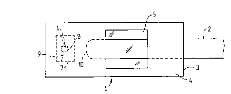
Figure 1 shows a laser diode 1 and a photosensitive
optical fibre 2 mounted within a container having a body 3
and a lid 4 in which is provided a window 5 substantially
transparent to W radiation. The method of fabricating this
intermediate product 6 will now be described.
A GaInAsP/InP buried hetero-structure laser diode is
grown in a conventional manner by MOVPE, and one facet of the
diode 8 is coated with multiple dielectric layers to reduce
its reflectivity.
With reference to Figure 1, the laser diode 1 is then
mounted on a heat sink 7, so that its coated facet 8, when
the diode is in use, emits radiation towards the fibre 2, and
elect=ical contact is made with the diode via wire bonds 9.
Before the fibre 2 is mounted within the container 3,
a lens 10 is formed at the end of the fibre.
In order to align the fibre 2 with the diode 1, the
remote end 11 of the fibre 2 is coupled to an optical power
meter I2 (shown in Figure 2) and the diode 1 is powered via
bond wires 9 so as to output a constant level of optical
radiation. Micro-posi tinning equipment 13 is then used to
manipulate the fibre 2 with respect to the diode 1 until a
maximum power reading on the power meter 12 is achieved. At
this point the fibre 2 is laser welded to the container 3,
thus ensuring stable, low loss optical coupling between the
diode 1 and the fibre 2.
The lid 4 is then hermetically sealed to the body 3 of
the container, ensuring that the window 5 in the lid 4 is
215379
WO 94117448 _ 8 _ PCT/GB94/00180
aligned above the fibre 2.
The window 5 is comprised of W grade silica quartz
which is substantially transparent to W radiation. The
window :gay alternative'_y be formed of any other material
which is substantially transparent at the wavelength at which
the grating is to be written. Preferably, the window 5 is
also transparent at visible wavelengths so that the grating
writing p_ rocess may be viewed at visible wavelengths. The
material of the window is optically flat on both sides, and
is of high optical quality so as not to introduce distortion
into an optical wavefront passing therethrough. The material
of the window should have good thermal stability so as to
avoi d i nhomogenei ti es i f he ati ng i s caus ed by s ome abs orbti on
of UV radiation.
This completes-the first stage of fabrication of the
external cavity semiconductor laser, and the packaged
intermediate product 6 may be stocked until required.
When a laser of a particular, preselected wavelength
is required an intermediate product 6 is taken from stock and
a reflection grating 15 at the appropriate pitch is written
into the fibre 2 of the intermediate product. Figure 3 shows
the arrangement used for writing this grating 15. The end 11
of the fibre 2 remote from the intermediate product 6 is
coupled to an optical spectrum analyser 14 so that both the
level and spectrum of the radiation output from the laser can
be monitored during the growth of the grating 15. In order
to write the grating 15 a standing wave interference pattern
is set up in the fibre core 16 by two suitably angled
ultraviolet beams of radiation 17 derived from the same
coherent source 18. The source 18 comprises an intra-cavity
frequency doubled Ar+ laser operating at 244nm, chosen because
of the sensitivity of the fibre 2 to this wavelength. It
will be appreciated that other writing wavelenths can be used
accordi::g to the variation in photosensitivity of the
particular fibre used with writing wavelength.
The two W beams 17 are produced by directing the
output of the source 18 onto a beamsplitter 19 which produces
215378
_ g _
two beams which are caused to converge on the fibre 2 by
mirrors 20. It will be appreciated that the pitch of the
resulting grating 15, and hence the wavelength of operation
of the laser, will be determined by the angle B at which the
two beams 17 intersect one another. The pitch of the grating
can thus be adjusted by altering the angle B, and is given
by
A =
2sin~6
where ~.1 is the wavelength of the source 18. The required
preselected wavelength of operation .18 of the external cavity
laser can then be achieved by choosing the pitch A in
accordance with
.1B = 2 ne A
ne is the effective mode index of the mode guided by the fibre
2 and is easily calculated by the skilled person for any
particular fibre 2 from a knowledge of the fibre refractive
index profile.
The photosensitive fibre 2 may be a germania doped
silica fibre fabricated in a non-oxidising atmosphere
according to the method of GB 9205090.5 (application no.
PCT/GB93/00462, publication no. W093/18420) filed on 9 March
1992. Alternatively the fibre may be co-doped with B203 in
accordance with GB 92305783.0 (publication no. W094/00784,
application no. PCT/GB93/01321 ) filed on 24 June 1992. It is
also possible that a standard telecommunications optical
fibre may have a sufficient level of photosensitivity to
comprise the fibre 2. The skilled person in this field will
be aware of the differing levels of photosensitivity
available from different fibre designs and will select a
fibre with a level of photosensitivity sufficient to achieve
the required level of reflectivity from the reflection
3 5 grati ng.
When utilising a CW power output from the source 18 of
approximately 20mW, and a Boron co-doped fibre, an exposure
time of several minutes is required. During the start of
AI~iENDED SHEET
I PEA/EP
- 10 -
this exposure period fine tuning of the grating pitch (by
altering the angle 8) ensures that the precise preselected
wavelength of the external cavity laser, as monitored by the
spectrum analyser 14, is achieved. Once the wavelength of
operation of the laser is equal to the preselected wavelength
the interference field is maintained without further
adjustment of the pitch of the grating 15.
The precise exposure time of the fibre 2, and thus the
level of reflectivity of the grating 15, is dependent on the
characteristics required prom the external cavity laser. If
for example high output power is required for a given drive
current thin the reflectivity of the grating 15 is chosen so
that optical feedback from the grating overcomes intra-cavity
losses, for example coupling losses between the fibre 2 and
the laser diode 1, while not being so high that it reduces
the output power of the external cavity laser. This is
achieved in the following manner. During the exposure time
~f the grating 15 the drive current to the laser diode 1 is
repeatedly tamped from zero to the maximum value of drive
current for the laser diode, and the output of the external
cavity laser against the drive current is monitored. Figure
4 shows a number of schematic L/I (light versus current)
characteristics of the laser during the growth of the
grating. Figure 4a shows the L/I characteristic at the
beginning of the exposure time when the grating 15 is
providing very little feedback to the laser diode 1. As the
grating 15 increases in reflectivity during the exposure
time, it provides more feedback to the laser diode 1 and the
L/I characteristic increases in gradient, as shown in Figures
4b and 4c. When the grating 15 provides sufficient feedback
to overcome the intra-cavity losses, the external cavity
laser reaches threshold and begins to lase. This is apparent
from the formation. of a knee in the L/I characteristic as
shown in Figure 4d. Once this knee in the L/I characteristic
is observed the drive current is no longer tamped, but is
fixed at the desired operating current Y of the external
cavity laser and the output of the laser at this driving
AMENDED SHEET
IPEA/EP
253?98
- l0A -
current is then monitored. This output increases with time,
as the reflectivity of the grating 15 continues to increase,
AMENDED SHEET
IPEA/EP
X15379&
JVO 94/17448 PCT/GB94/00180
- 11 -
towards a peak, as shown in Figure 4e. Stopping the exposure
of the grating at this peak will result in an external cavity
laser having an output power optimised to the chosen drive
current. If the exposure of the grating is continued beyond
this point the resulting higher level of feedback will cause
the output of the laser to be reduced, as shown in Figure 4e.
It should be noted that neither the coupling loss
between the fibre 2 and the grating 15, nor the level of
reflectivity of the grating need be calculated, estimated, or
measured, in contrast to prior art methods in which the
grating is written before the fibre is aligned to the laser
di ode 1.
Since the grating 15 is written in the fibre 2 only
after packaging in the container 3 there is no danger that
the wavelength of operation of the grating will ~be altered
for example by any stress caused to the fibre during laser
welding and packaging. Furthermore the optimum reflectivity
of the grating 15, to overcome coupling losses between the
laser diode 1 and the fibre 2, while not being so high as to
limit the output of the laser, can be achieved only through
writing of the grating after packaging, when coupling losses
are fixed.
It will be appreciated that desired characteristics,
other than an optimised output power, may be achieved during
the grating writing, which will require different aspects of
the laser performance to be monitored. For example, a
certain specified output power at a particular drive current
may be required, or a particular laser linewidth, or
threshold may be required.
A second embodiment of the present invention
comprising a planar waveguide Mach Zehnder (MZ) band-pass
filter will now be described.
Many telecommunications applications require the use
of a band-pass rather than a band-stop filter. The band-stop
characteristic of a reflection grating written into a
photosensitive waveguide, as described above, can be
transformed to a band-pass characteristic by incorporating an
WO 94117448 ~ ~ ~ ~ PCT/GB94/00180
- 12 -
identical such reflection grating into each of the two arms
of a balanced MZ interferometer.
The MZ band-pass filter is fabricated in two stages.
The first stage of fabrication results in a balanced MZ
interferometer packaged in a container according to the
present invention. This intermediate product is then stored
until a requirement for a band-pass filter of a particular
wavelength and bandwidth arises. The second stage of
fabrication comprises a first step of writing a grating into
each of the two arms of the MZ, and a second step of trimming
the interferometer to ensure that both arms are balanced.
Both these steps are carried out by passing W radiation
through the window in the package.
With reference to Figure 5 a balanced MZ
interferometer is formed by fabricating two identical 50:50
waveguide couplers 21, 22, at 1555nm, on the same substrate
23 using the well known flame hydrolysis technique. The
output ports of the coupler 21 are joined to the input port
of the coupler 22, so forming two arms 24 and 25 of the MZ
interferometer, each arm being approximately lOmm in length.
In order to achieve a balanced MZ structure these two
arms 24 and 25 must be substantially of equal optical path
length. The optical path length of each arm is affected by
both the refractive index of the waveguide forming the arm
and the physical length of the arm. Fluctuations in the
refractive index of waveguides formed by flame hydrolysis,
and thus of the effective mode index of optical frequencies
guided by them are relatively small - being of the order of
one percent of the effective mode index. These fluctuations
are moreover in practise largely averaged over the length of
each arm so that the physical differences in arm length are
the major cause of differences in optical path length between
the arms. Using photolithographic techniques, the physical
length of the arms 24 and 25 can be defined to within a few
microns, resulting in an optical path difference between the
arms of less than a few wavelengths, and hence a balanced MZ
structure.
_ . _ ._ _...__.. T
3 _ 2 i 5379$
after these waveguides have been formed in a
conventional manner by the flame hydrolysis technique, they
are sub~ected.to_a final hydrogenation process in accordance
with World Patent 93/18420 to ensure that they are photosensitive .
The substrate 23 is then mounted in the body 26 of a
container and fibres 27 are aligned with each of the ports
28, 29, 30 and 31 of the MZ interferometer and laser welded
to the body 26. A lid 32 having a window 33, transparent to
W radiation, is then =aser welded to the body 26 of the
container, ensuring that the window 33 is aligned above the
arms 24, 25 of the MZ interferometer. This completes the
first stage of fabrication, and the resulting intermediate
product is stored.
When a band-pass filter is required at a particular
wavelength and having a particular bandwidth pass-band, for
example 1.5558~m and Inm, an intermediate product is exposed
to W radiation to give a MZ band-pass filter having the
desired characteristics:- This second stage of fabrication
comprises two steps. Firstly, an identical grating is
wri tten i nto each arm 24 and 25 of the MZ interferometer, and
secondly the interferometer is trimmed so as to ensure it is
still balanced and to ma.~cimise the performance of the fil ter.
The gratings are written, using the same apparatus
previously described in relation to the first embodiment of
the invention, into each arm 24, 25 of the interferometer,
close to one of the couplers 22, as shown in Figure 5. The
pitch, length and death oz refractive index modulation of the
gratings are chosen in conventional manner to give the
desired band-pass characteristic i.e. centre wavelength,
bandwidth and transmission coefficient.
Typical exposure times range between seconds to
several minutes. Gracing lengths are around 3mm. The
gratings are written by aligning the waveguides to the UV
laser stripe while viewing under a microscope. Typical blue
luminescence is observed when the Ge core is illuminated with
U'J radiation. It is estimated from previous writing times
AI~IEaDED SHEET
IPEA/EP
2~~3~~8
_ WO 94117448 PCT/GB94/00180
- 14 -
that the reflectivity of each grating is over 90%.
A fused tapered 3dB fibre coupler 34 is spliced to the
fibre 27, coupled to the port 28 of the MZ interferometer, to
allow a broad bandwidth ELED (Edge-Emitting LED) 35,
operating around a peak wavelength of 1550nm, to be launched
into the MZ, and, simultaneously, any back reflection from
the MZ emerging from port 28 to be monitored.
SABLE 1
% of total output power
BEFORE AFTER
gORT# TRI MMI NG TRI MMI NG
28 Band-pass at 1. 5558~m 54. 3 [ 64. 7 J 9. 8 [ 13. 3 J
29 Looped Band-pass at 1. 5558~m 24. 6 [ 28. 9 J 58. 8 [80. 3 )
30 Band-stop minimum 2. 8 2. 2
30 Band-pass crossed 70.7 70. 7
31 Band-pas s through 4. 8 2. 6
31 Band-stop minimum ~ 0. 13 0.08
(Note: Measurements are with reference to the power in
the fibre at the input port 28: no allowance has been
made for the coupling loss from the fibre to the
waveguide at port 28. The transfer characteristics are
therefore better than the quoted figures. The figures in
brackets are relative to the total power appearing at the
output ports 30 and 31. A fibre-fibre loss from port 28
to port 30 of 1. 35dB was measured. )
The four ports of the Mach-Zehnder are measured
immediately after writing the two gratings. Table 1 shows
the measured data at all four ports as a fraction of the
power in the fibre at port 28. In order to make comparison
of the signal in all four ports, each port has been
referenced to the total power measured in the fibre offered
to port 28. The launch efficiency into port 28 is not known
exactly, however the power exiting ports 30 and 31 are known
and thus the total insertion loss including propagation loss
and launch efficiency can be inferred. Also, accurately
known are the reflections of the gratings from the extinction
2153'798
- 15 -
measurements at the output ports 30 and 31. Since the exact
power in the input waveguide is not known and the launch is
not fully optimised, the final values include any propagation
and coupling losses, and are worse than a true indication of
the performance. The reflection from the gratings appears as
a 'drop-out' (Band-stop) in the spectrum of port 30 at a
wavelength of 1.5558~m, the dip corresponding to a 95.50
reflection (13.5dB rejection). The remaining wavelengths
within the spectrum are transmitted at port 31 and appear as
broad pass bands around the Band-stop with transmission of
only 4.8% of the total power at the input. The peak
reflected signal (the band-pass) in port 28 at 1.5558~m is
54.30 of the total power at the input after allowing for the
3dB loss of the coupler at port 28. Port 29 (the looped-
through port) shows the reflection in band-pass with the peak
transmission of 24.60 of the power at the input.
It is clear that the reflected signals from the
interferometer are unbalanced at the input coupler 21 of the
MZ since the desired band-pass output is required at port 29
rather than port 28. To remedy this, the MZ is trimmed by
re-exposing one of the arms (say the arm 24) of the MZ to a
single unmodulated beam of W-radiation in the path
immediately after the input coupler 21 to change the local
refractive index 36, as shown in Figure 5. The input port 28
is monitored in situ in order to minimise the reflection.
The results of this exposure are shown in the sequence (a)-
(c) in Figure 6. The spectra shown are for increasing
exposure, over a 2mm region. It can be seen that in under
two seconds of exposure, the light reflected in port 28 is
reduced by approximately SdB. The effect of W exposure of
the other arm 25 for 0.04 seconds can be seen in Figure 6
(d). The reflected signal has gone up by more than 2dB,
showing that the change in coupling due to the previous
exposure is being reversed. The final Figure 6(e) shows the
spectrum after re-exposure of the first arm for another 1/2
second.
The index change estimated from the change in coupling in
AMENDED SHEET
IPEA/EP
WO 94/17448 ~ ~ ~ ~ PCTlGB94/00180
- 16 -
2. 4 seconds of W exposure in these measurements of the MZ is
-4. 4 X 10-°. The balanced. MZ band-pass filter is then tested
for transmission characteristics. The spectra from the four
ports are shown in Figure 7. The signal in port 28 has been
reduced from 54.3% of the power in the fibre at port 28 to
about 9.76%. The band-pass in the looped through port 29
signal has increased from 24. 6% to 58. 8%. The signal in port
31 has gone down from 4. 8 to 2. 8%. The latter split could
not, in this case, be altered since the gratings are written
close to one coupler and no space is available between the
gratings and the coupler to alter the phase in one arm of the
interferometer. The bandwidth of the band-stop/pass due to
the grazing is approximately lnm, in good agreement with the
calculation from the exposed lengths.
Thus, it can be seen that, by employing a package having
a W transparent window, not only can the precise desired
characteristics of a band-pass filter be achieved by a simple
second fabrication stage, but the performance of the filter
can also be optimised. Hence, demand for an infinite range
of different filters can be met from a small stock of
intermediate products packaged according to the present
i nventi on.
It will be appreciated that the method and package of the
present invention find wide application within the
telecommunications field, and can advantageously be employed,
not only for the packaging of single optical devices, but
also for the packaging of opto-electronic integrated
circuits. Complex opto-electronic integrated circuits,
implemented for example on planar silica substrates,
comprising lasers, couplers, amplifiers and filters will
benefit from the application of the present invention. In
accordance with the present invention, the functionality of
such integrated circuits could be defined after packaging to
yield for example a multi-wavelength source or a wavelength
comb generator.
Following the definition of the function the optical
device, whether as an external cavity laser, a Mach-Zehnder
_ T
2153°98
vV0 94/17448 PCT/GB94/00180
- 17 -
filter or otherwise, it may be desirable to prevent further
electro-magnetic radiation from reaching the photosensitive
part of the optical device e. g. by covering the window in the
container with a light-proof paint or sticker.