Note : Les descriptions sont présentées dans la langue officielle dans laquelle elles ont été soumises.
~1~4814
-1 RCA 87,613
AMPLIFIER FOR SCANNING BEAM VELOCITY MODULATION
This invention relates generally to scanning beam velocity
modulation (SVM), and more particularly to an amplifying circuit
employed therein.
BACKGROUND OF THE INVENTION
It is known that apparent picture sharpness may be
enhanced by modulation of the scanning beam velocity in accordance
with a derivative of a video display signal. The derivative signal, or
SVM signal, may be derived from a luminance component of the video
display signal and is employed to produce scanning beam velocity
variations. Slowing of the electron beam velocity results in
brightening of the display, acceleration of the velocity results in
display darkening. Thus, horizontal rate edges may be visually
enhanced by a variation of the display intensity about an edge
transition. This method of sharpness enhancement provides various
advantages over that provided by video frequency peaking, for
example, blooming of peaked high luminance picture elements is
avoided, and additionally, video noise occurring within the bandwidth
of a video peaker is not enhanced.
2 0 Scanning beam velocity may be modulated by an SVM coil
which generates a supplementary deflection field. The SVM field, in
conjunction with the main deflection field, produces electron beam
acceleration or deceleration responsive to the polarity of current in the
SVM coil. The amount of beam acceleration or deceleration is
2 5 proportional to the magnitude of the SVM current. The deflection
sensitivity of a typical SVM coil, may for example, be in the range
where 1 ampere produces between 1 to 3 millimeters of beam
deflection at center screen.
Since the SVM signal generally represents high frequency
3 0 video content, it can be appreciated that the SVM coil current has a
magnitude and frequency spectrum which is readily coupled to
produce unwanted, extraneous crosstalk components. Such crosstalk
components may result from coupling via the power supply and or
return circuit. Hence it is advantageous to arrange that SVM coil
3 5 current be generated and circulate without significant ground or
power supply conduction.
SUMMARY OF THE INVENTION
An apparatus for electron beam deflection comprises a
cathode ray tube having a scanning electron beam. A coil for
_~1~4~14
RCA 87,613
supplementary electron beam deflection is mounted on the cathode
ray tube. An amplifier is coupled between a supply of power and a
return circuit and has an input coupled to a signal representing a
video signal edge transition. The amplifier has an output which is
coupled to the coil for generating a pulse current therein for
electron beam deflection responsive to the signal. The amplifier
and the coil are configured for circulation of the pulse current
mainly within the coil and amplifier output without substantial
pulse current flowing in the power supply and return circuit.
1 0 BRIEF DESCRIPTION OF THE DRAWING
FIGURE 1 illustrates an inventive scanning beam
velocity modulation drive amplifier and auxiliary deflection coil.
FIGURE 2 illustrates the SVM coil driver of FIGURE 1
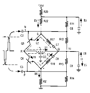
depicted in a symmetrical bridge configuration.
1 S FIGURE 3A, 3B,and 3C illustrate an SVM signal and currents
generated thereby.
FIGURE 4 illustrates an inventive modification to the
circuit of FIGURE l, depicted as a bridge configuration.
DETAILED DESCRIPTION
2 0 In FIGURE 1 a scanning beam velocity modulation ~ signal
or SVM signal, is input between terminals A and B. The SVM signal
at terminal A is depicted for illustrative purposes as an impulse
like waveform, having symmetrical peak to peak value of 1.5 volts.
The derivation and processing of the SVM signal form no part of
2 5 this application. The low side, or signal ground conductor from the
SVM signal generator is coupled to the drive amplifier signal
ground via a resistor to prevent unwanted coupling of transient
interference or noise etc. The signal ground conductors shown in
FIGURES 1 and 2 are all connected to a deflection ground conductor.
3 0 The inventive drive amplifier of FIGURE 1 may be
considered to comprise an amplifier and coring section 100, with a
voltage gain of approximately 5 and an auxiliary deflection coil
drive amplifier 200, configured essentially symmetrically about a
voltage Vc, established mid way between the power supply and the
3 5 driver ground. The AC coupled input signals at N and P are also
symmetrically biased about voltage Vc for coupling to the
complementary drive transistors. The auxiliary deflection or SVM
coil is coupled between voltage Vc at point Q, and the junction of
the drive transistor collectors, point R. The driver transistors are
3 215 ~ g 14 RCA 87,613
biased in class B such that negative transitions of the SVM signal
cause conduction in the PNP transistor and positive signal
transitions turn on the NPN transistor. Thus bidirectional deflection
current is driven through the SVM coil from the collectors to circuit
point Q, with an insignificantly small current component circulating
outside the respective collector to emitter circuits. To provide
control of power dissipation, particularly in the driver stage, feed
back is provided from an emitter current sample. This attenuated
and filtered signal SVM CTL is coupled to an SVM signal processing
circuit which forms no part of this application.
The nominally 1.5 volt peak to peak SVM signal is input
at terminal A with the SVM processor signal ground coupled to
terminal B to reduce spurious and unwanted transient ground
current crosstalk or noise. The signal at terminal A is coupled via a
1 S resistor R1 to the base of an NPN transistor Q1, which is configured
as a common emitter amplifier with a gain of approximately 5. The
emitter of transistor Q1 is connected to a series combination of
resistor R3 and resistor R4 which are connected to ground, with the
junction, terminal B, connected to the SVM processor ground. The
2 0 collector of transistor Q1 is connected via a resistor R2 to a power
supply, for example, 26 volts which is decoupled by series resistor
R7 and decoupling capacitor Cl. The collector of transistor Q1 is
also coupled to the base terminal of an NPN transistor Q2,
configured as an emitter follower amplifier. The collector of
2 5 transistor Q2 is connected to the decoupled 26 volt power supply
and the emitter is connected directly to a base terminal of an NPN
transistor Q3. The emitter of transistor Q2 is also connected to a
resistor RS and a resistor R6, connected in series with resistor R6
connected to ground. The junction of the resistors is connected to
3 0 the base terminal of an PNP transistor Q4. Transistors Q3 and Q4
are configured as emitter follower amplifiers where the SVM signal
at the base of transistor Q4 has a DC offset with respect to the base
of transistor Q3, as a result of current flow in resistor R5. This DC
offset introduces coring or small signal amplitude attenuation of the
3 5 SVM signal. The emitter of transistor Q3 is coupled via a resistor
R8 to an AC coupling capacitor C2, and similarly the emitter of
transistor Q4 is coupled via a resistor R10 to an AC coupling
capacitor C3. The emitters of transistors Q3 and Q4 are connected
together via a resistor R9 which provides control of RFI generation.
RCA 87,613
The SVM signal at capacitor C2 is filtered for RFI reduction by a
capacitor C4, connected to ground. The signal at capacitor C3 is RFI
filtered by a capacitor CS connected to ground. The base terminal
of PNP driver transistor QS is connected to the junction of
capacitors C2 and C4 and the junction of resistors R11 and R12.
Similarly for the base terminal of NPN driver transistor Q6 which is
connected to the junction of capacitors C3, CS and resistors R13 and
R14.
Resistors R 11, R 12, R 13 and R 14 form a series connected
potential divider coupled between a supply voltage +V and ground.
The supply voltage +V, for example approximately 135 volts is
decoupled by a series resistor R20 and a bypass capacitor C6, which
is connected to ground. Since the potential divider formed by
resistors R11, R12, R13 and R14 is symmetrical, the center point Q
at the junction of resistors R12 and R13, generates a voltage Vc
having a value of half that of voltage +V, for example
approximately 67 volts, which is decoupled to ground by capacitor
C8. The emitter of PNP transistor QS is also coupled to center point
Q, via a series connected capacitor C7 and resistor R17. Similarly
2 0 the emitter of NPN transistor Q6 is coupled to the junction of
resistors R12 and R13 via a series connected capacitor C9 and
resistor R19. These two series coupled feedback paths effectively
reduce the AC impedance at center point Q. The emitter of PNP
transistor QS is connected to the 135 volt power supply via series
2 5 connected resistors R22 and R20. Resistor R20 provides decoupling
from the power supply as described. Resistor R22 at the emitter of
transistor QS provides DC degeneration to control the DC operating
point. Similarly the emitter of NPN transistor Q6 is connected to
ground via resistor R21 for control of the DC operating point.
3 0 The SVM coil L is positioned on the CRT tube neck and
may be in close proximity to a signal ground or a low impedance
conductor, for example a main deflection yoke LX. Such close
proximity conductors provide stray coupling capacitance, depicted
by capacitor CS, which not only impairs SVM performance by
3 5 degrading the rise time of the of the coil current but additionally
may provide an interference or crosstalk coupling path for the high
frequency, impulsive SVM coil current. The nature of the SVM
current is conducive to radiation and capacitive coupling into
adjacent conductors. Furthermore it is very desirable that the
5_ ~~t~4814 RCA87,613
impulsive SVM current be excluded from the power supply and
return current paths such as ground conductors. Unwanted SVM
interference may be injected into circuitry where the signal
components are advanced or earlier than the video signal from
which the SVM drive signal is generated. Thus the unwanted
crosstalk signal or glitch is not hidden but is visible, anticipating the
sharpness enhancing action of the SVM circuitry. Accordingly, as
SVM operational frequencies are raised and drive currents are
increased, it is increasingly important that the impulsive SVM drive
currents be confined to the drive amplifier and auxiliary deflection
or SVM coil.
FIGURE 2 shows the inventive SVM amplifier of FIGURE
1 redrawn to illustrate circuit 200 topologically as a symmetrical
bridge. The bridge is illustrated with nodes S and T, and R and Q,
corresponding to the same nodes shown in FIGURE 1, where nodes S
and T are coupled between the 135 volt supply and ground
respectively. The emitter of transistor Q5, node S, is coupled to the
power supply via resistors R22 and R20 and is decoupled to ground
by capacitor C6. Node T, at transistor Q6 emitter is coupled to
2 0 ground via resistor R21. The collectors of transistors QS and Q6 are
joined and form drive node R of the bridge, with the auxiliary
deflection or SVM coil connected across the center of the bridge to
node Q. The tuning and damping components connected in parallel
with SVM coil L, have been omitted for clarity. Node Q is decoupled
2 5 to ground by a capacitor C8 and is DC biased to approximately half
the supply voltage, for example 67 volts, by the resistive divider
formed by series resistors R11, R12, R13 and R14. In the emitter
circuitry of transistor QS are series connected capacitor C7 and
resistor R17 which are connected to node Q. An identical series
3 0 connected network formed by resistor R19 and capacitor C9 is
connected from transistor Q6 emitter to node Q. Thus transistors QS
and Q6 form one side of the bridge with the series connected
capacitor .and resistor networks forming the other side.
Typically in bridge configured circuitry, current may
3 5 flow between opposite nodes, for example R and Q, without
significant interaction with currents flowing between the other
opposing nodes, for example S and T. Thus, SVM coil current flow
between nodes R and T is confined to circulate largely within the
bridge circuit and is largely absent from the power supply and
6 _ 2 ~ ~ 4 814 RCA 87,613
ground. Hence high frequency impulsive SVM currents are
prevented from potentially interfering conduction via the power
supply or return.
The processed and amplified SVM signals are AC coupled
to the bridge configured driver transistors QS and Q6 via capacitors
C2 and C3 respectively. Transistors QS and Q6 operate as class B
amplifiers with the bases biased at cut off by the resistive divider
R11, R12, R13 and R14. Transistors QS and Q6 may be biased
further off by suitable manipulation of the resistor values if
additional signal coring is required. A negative SVM signal impulse
at point N causes transistor QS to conduct and cause an impulsive
current I1 to circulate via the S VM coil to node Q, and capacitors C7,
C8, C9 and CS. Current I1 comprises essentially two parts, where I1
- I2 + I3, where I2 circulates within the bridge and current I3 is
1 5 conducted through the coil via capacitors CS and C8 and returning
via capacitor C6 and resistor R22. When transistor QS turns on, a
low impedance circuit is formed causing current sourced by C7 to
circulate through SVM coil L and series connected resistor R17.
Since the value of resistor R17, 3.3 ohms is small compared with
2 0 the value of resistor R22, 51 ohms, current I2 is large compared to
current I3. For example, with the values indicated in FIGURE 1, I3
is approximately 1/15 that of current I2. The duration of transistor
QS conduction is determined by the width of the SVM impulse,
which for example may be 150 nanoseconds. Thus when transistor
2 5 QS is conducting a discharge path is formed having a discharge time
constant, due to resistor R17 and capacitor C7, of approximately 75
microseconds, ignoring the saturation resistance of transistor Q5.
Hence, since capacitor C7 sources SVM current for only about 150
nanoseconds the voltage across the capacitor is not significantly
3 0 changed or discharged. Capacitor C8 also sources a 150
nanoseconds current pulse via the SVM coil, transistor Q5, resistor
R22 and capacitor C6, which appears in series as current I3. Stray
capacitor CS is also discharged via a current path through ground
and capacitors C6 and C8. However, since the value of stray
3 5 capacitance is minuscule in comparison to capacitors C6, C7, C8 and
C9, being in the order of 25 picofarad, the stray conducted SVM
current is also minuscule in comparison to the current circulating
within the bridge. Typically current I1 has a peak value in the
order of 600 milliamperes, with I3 being typically 40 milliamperes.
21 ~ 4 814 RCA 87,613
A positive SVM signal impulse at point P causes
transistor Q6 to conduct an impulse current I6 from node Q, via
SVM coil L, being sourced essentially by capacitor C9. The current
conducted by transistor Q6 to SVM coil L comprises essentially two
components I6 = I7 + I8, where I7 circulates within the bridge and
current I8 is conducted through the coil via capacitors CS and
resistor R21 and returns via capacitor C8. Since the value of
resistor R19, 3.3 ohms, is small compared with the value of resistor
R22, 51 ohms, current I7 is large compared to current I8, thus I8
has a value approximately 1/15 that of I7. SVM Current conducted
via stray capacitance CS circulates through ground and C8. Any
reduction in stray capacitance CS directly reduces the magnitude of
ground conducted currents I3 and I8. The discharge time constant
formed by resistor R19 and capacitor C9 functions as described for
transistor Q5. Since transistor Q6 conducts for approximately 150
nanoseconds, which corresponds to approximately 1/500 of
discharge time constant, there is no appreciable change in the
voltage across capacitor C9.
FIGURE 3A depicts a "pulse and bar" video signal
2 0 occurring during the horizontal period of one TV line. FIGURE 3B
illustrates an SVM signal at terminal A of FIGURE 1, comprised
essentially of edges, or horizontal transitions, derived from the
signal shown in FIGURE 3A but depicted with an expanded time
scale. FIGURE 3C depicts voltage and current pulses occurring at
2 5 times t1 and t2 but with an expanded time scale. Waveform P
depicts the SVM voltage waveform occuring at point P, which is
coupled to cause SVM current conduction in transistor Q6. The
signal waveform depicted in P is identical to the signal applied at
circuit point N in FIGURE1, and results in SVM current conduction
3 0 for negative signal values. Waveform I6 shows the collector
current of transistor Q6 circulating within the bridge components,
SVM coil L, resistor R19 and capacitor C9. Waveform I8 shows the
current out of the bridge circuit during transistor Q6 conduction
which is approximately 1115 that of collector current I6.
3 5 FIGURE 4 shows an inventive modification to the bridge
configured SVM amplifier of FIGURE 2. In FIGURE 4, nodes S and T
are relocated to the junctions of the series feedback networks
comprising resistor R17 and capacitor C7 and resistor R19 and
capacitor C9 respectively. The circuit operation remains largely as
21 ~ 4 ~ 14 RCA 87,613
w described for FIGURE 2. However, in the embodiment shown in
FIGURE 4, conduction in either transistor QS or Q6, responsive to the
appropriate polarity of input signal, causes impulsive currents to be
sourced by capacitor C7 or C9. For example, a negative going input
pulse, typically having a duration in the order of 150 nanoseconds,
causes transistor QS to conduct current from capacitor C7 via
resistor R17 and the SVM coil. Impulsive currents I1 and I2 are
essential equal and impulse current I3 is substantially reduced and
essentially comprises current due to stray capacity CS. The inpulse
current sourced by capacitor C7 is recharged via resistor R22 when
transistor QS is non-conducting. Similarly for transistor Q6, where
a positive input impulse causes transistor Q6 to conduct current
from capacitor C9 via resistor R19 and the SVM coil. Discharge
currents I6 and I7 are essentially equal, and current I8 is
1 5 essentially due to stray capacity CS. Capacitor C9 is recharged
during periods of non-conduction of transistor Q6 via resistor R21.
Thus the embodiment of FIGURE 4 generates impulse or SVM
currents which circulate within the bridge and are essentially
absent from the power supply and return.
2 0 The inventive bridge configured SVM coil drive
amplifier confines impulsive current to circulate largely within the
bridge circuit, hence high frequency SVM currents are largely
prevented from potentially interfering conduction via the power
supply or power return.