Note : Les descriptions sont présentées dans la langue officielle dans laquelle elles ont été soumises.
21S~968
Title of the Invention
POWER CONTROL CIRCUIT FOR USE WITH TRANSMITTER
BACKGROUND OF THE INVENTION
The present invention relates to a power control circuit
for use with a transmitter, in particular, to a power control
circuit having a power amplifier for linearly amplifying a
signal and outputting the amplified signal.
In for example an AM modulating method of a transmitting
system, the control of power fluctuation of a transmission
signal may be an important factor for improving the
performance. A transmitter used in such a transmission
system has an RF (Radio Frequency) power amplifier that
linearly amplifies a signal and outputs the amplified signal.
In addition, the RF power amplifier should amplify a
signal in a linear region so as to prevent the signal from
distorting.
However, due to various causes such as a temperature
change, the gain of a pre-stage amplifier of the RF power
amplifier may fluctuate, thereby causing the input level of
the RF power amplifier to fluctuate. If the RF power
amplifier operates in the saturation region due to the
fluctuation, it cannot linearly amplify the input signal.
Thus, since the signal largely distorts, required spurious
standard cannot be satisfied.
To solve this problem, a saturation preventing control
loop method is known. In this control method, an output
~ - 2154968
signal of the RF power amplifier is detected. The detected
output voltage is compared with a reference voltage. The pre-
stage variable gain amplifier is controlled corresponding to
the relation between the output voltage and the reference
voltage. Thus, the output power of the RF power amplifier is
controlled so that the RF power amplifier does not operate in
the saturation region. Fig. 1 is a schematic diagram showing
the construction of a circuit according to this control
method.
In the power control circuit according to the
saturation preventing control loop method, a modulated signal
that includes speech information and the like that are input
from an input terminal 1 is amplified by a variable gain
amplifier 2. The amplified signal is supplied to an RF power
amplifier 3. The RF power amplifier 3 amplifies the input
signal with a predetermined amplitude. The amplified
modulated signal is supplied from the RP power amplifier 3 to
a signal output terminal 5 through a directional coupler 4.
The directional coupler 4 extracts a part of the modulated
signal. The extracted modulated signal is detected by a
detecting circuit 6. A comparator 8 compares the level of the
detected signal with a predetermined reference voltage
supplied from a reference voltage supply terminal 7. The
compared result of the comparator 8 is fed back to the gain of
the variable gain amplifier 2. Thus, the level of the
modulated signal that is supplied from the variable gain
amplifier 2 is adjusted.
27598-99
215496 8
In other words, when the level of the detected signal is
higher than the reference voltage, the gain of the variable
gain amplifier 2 is decreased so as to decrease the level of
the modulated signal that is supplied to the RF power
amplifier 3. When the level of the detected signal is lower
than the reference voltage, the gain of the variable gain
amplifier 2 is increased so as to increase the level of the
modulated signal that is supplied to the RF power amplifier
3.
The saturation preventing control loop 20 always
properly maintains the level of the modulated signal that is
supplied to the RF power amplifier 3, thereby preventing the
RF power amplifier 3 from operating in the saturation region.
However, the circuit shown in Fig. 1 only controls the
output power of the saturation preventing control loop method
corresponding to the reference voltage supplied from the
reference voltage supply terminal 7.
For example, as in a CDMA (Code Division Multiple
Access) cellular system that should control transmission
power for maintaining the maximum system capacity, the above-
described variable gain amplifier should have a control
signal corresponding to the required transmission power.
However, in the circuit shown in Fig. 1, the
transmission power can be controlled corresponding to the
reference voltage supplied to the reference voltage supply
terminal 7. In this method, however, due to the response
time and output power detecting characteristics of the loop,
21S4968
the system standard cannot be adequately satisfied.
The present invention is made to solve such a problem.
An object of the present invention is to prevent an RF power
amplifier of a conventional saturation preventing control
loop method from saturating in the case that the system
transmits a signal with maximum power and to disconnect the
saturation preventing loop for controlling the transmission
power in the case that the system transmits a signal without
the maximum power so as to satisfy characteristics required
for the power control method of the system.
SUMMARY OF THE INVENTION
In a transmission power control system such as a CDMA
cellular system, when the transmission power of an RF power
amplifier almost exceeds the maximum transmission power, a
saturation preventing control loop should be activated.
Otherwise, the output power of the RF power amplifier should
be controlled corresponding to the transmission power control
method of the system.
Thus, the power control circuit of the present invention
has a variable gain amplifier including an input terminal for
inputting a signal to be transmitted, an output terminal for
outputting an amplified signal of the input signal, and a
gain control terminal for inputting a gain control signal.
The amplitude of the input signal is controlled corresponding
to the gain control signal. A detecting portion detects the
level of the signal amplified by the variable gain amplifier.
-- 2154968
A comparing portion compares the level of the amplified
signal with a predetermined reference value.
One terminal of a switch is connected to an output
terminal of the comparing portion. The other terminal of the
switch is connected to an adder. When the level of the
amplified signal is larger than the reference value, the
switch is turned on. When the level of the amplified signal
is smaller than the reference value, the switch is turned
off.
In addition, a system power control terminal for
supplying a system power control signal is connected to the
adder. The adder outputs a gain control signal of which the
output signal of the system power control terminal and the
output signal of the other terminal of the switch are added
as a gain control signal. The output signal of the adder is
supplied to a gain control terminal of the variable gain
amplifier.
The power control circuit has a variable gain amplifier
and a summing amplifier. The variable gain amplifier
includes an input terminal for inputting a signal, an OUtpllt
terminal for outputting a linearly amplified signal of the
input signal, and a gain control terminal for inputting a
gain control signal. The variable gain amplifier controls
the amplitude of the input signal corresponding to the gain
control signal. The summing amplifier includes a plurality
of system power control terminals for inputting a plurality
of system power controL signals corresponding to
27598-99
215~968
predetermined characteristics such as those of the CDMA
system. The adding circuit adds these system power control
signals and outputs a gain control signal. The range of the
input voltage of the system power control signal is converted
so that the adding operation of the adding circuit is
performed in a linear region.
These and other objects, features and advantages of the
present invention will become more apparent in light of the
following detailed description of best mode embodiments
thereof, as illustrated in the accompanying drawings.
BRIEF DESCRIPTION OF DRAWINGS
Fig. 1 is a circuit diagram showing the construction of
a conventional power control circuit;
Fig. 2 is a block diagram for explaining the
construction of a power control circuit according to a first
embodiment of the present invention;
Fig. 3 is a block diagram showing connections of the
power control circuit according to the first embodiment and
another circuit;
Fig. 4 is a circuit diagram showing the construction of
a transmission power control block 31 of the power control
circuit of Fig. 2; and
Fig. 5 is a graph showing an operation region of an OP
amplifier U2.
DETAILED DESCRIPTION OF THE PREFERRED EMBODIMENTS
~13~9~
Next, with reference to Figs. 2 and 3, a first
embodiment of the present invention will be described. Fig. 2
is a circuit diagram showing the construction of a power
control circuit according to the present invention. Fig. 3 is
a block diagram showing connections of the power control
circuit of Fig. 2 and other circuits.
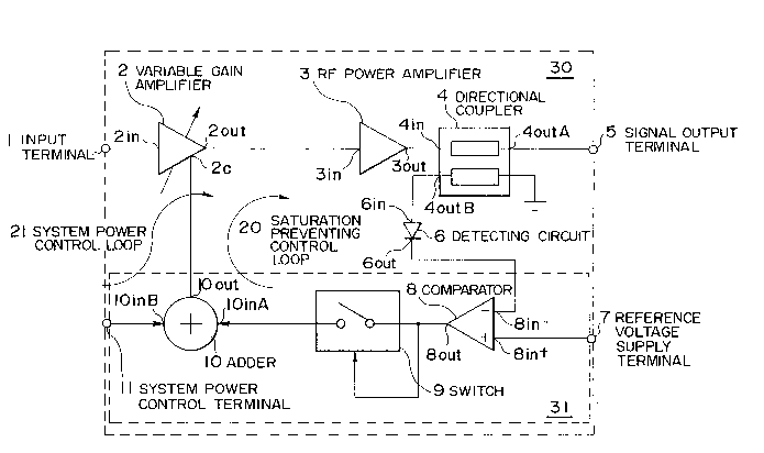
In the power control circuit 30, an input terminal
2in of a variable gain amplifier 2 is connected to an input
terminal 1. An output terminal 20ut of the variable gain
amplifier 2 is connected to an input terminal 3in of an RF
power amplifier 3 through another amplifier, a filter, a
mixer, and so forth (not shown).
An output terminal 30ut of the RF power amplifier 3
is connected to an input terminal 4in of a directional coupler
4. One output terminal 40utA of the directional coupler 4 is
connected to a signal output terminal 5. Another output
terminal 40utB of the directional coupler 4 is connected to an
input terminal 6in of a detecting circuit 6. An output
terminal 60ut of the detecting circuit 6 is connected to a
negative input terminal 8in- of a comparator 8.
A reference voltage supply terminal 7 is connected
to a positive input terminal 8in+ of the comparator 8. One
terminal of a switch 9 is connected to an output terminal 80ut
of the comparator 8. When the signal level of an output
signal from the output terminal 80ut is "L", the switch 9 is
turned on. On the other hand, when the signal level is "H",
the switch is turned off.
27598-99
215~968
Another terminal of the switch 9 is connected to one
input terminal 10inA of an adder 10. An output terminal
10out of the adder 10 is connected to a control terminal 2c
of the variable gain amplifier 2.
The above-described variable gain amplifier 2, the RF
power amplifier 3, the directional coupler 4, the detecting
circuit 6, the comparator 8, the switch 9, the adder 10, and
so forth construct a saturation preventing control loop 20.
On the other hand, a system power control terminal 11 is
connected to another input terminal 10inB of the adder 10.
The system power control terminal 11, the adder 10, the
variable gain amplifier 2, and so forth construct a system
power control loop 21.
A reference voltage control circuit 40 is connected to
the signal output terminal 5. The reference voltage control
circuit 40 detects the output power of the signal output
terminal 5 and varies the reference voltage supplied to the
reference voltage supply terminal 7 corresponding to the
detected result.
A system power control circuit 50 is connected to the
system power control terminal 11. The system power control
circuit 50 generates a predetermined system power control
signal for controlling the power of the system.
Next, the operation of the power control circuit 30 will
be described.
The designating operation of the saturation preventing
control loop for preventing the RF power amplifier from
~ 54968
saturating will be described. In this operation, the value of
the reference voltage supplied to the reference voltage supply
terminal 7 is designated so that the maximum transmission
power is in a linear region of the RF power amplifier 3.
The variable gain amplifier 2 amplifies the
modulated signal that is supplied from the input terminal 1
with a predetermined amplitude. The amplified signal with the
maximum power is supplied to the RF power amplifier 3 through
another amplifier, a filter, a mixer, and so forth (not
shown).
Thus, the modulated signal is amplified by the RF
power amplifier 3 regardless of whether or not the RF power
amplifier 3 operates in the saturation range. The resultant
signal with the maximum power is supplied from the signal
output terminal 5 through the directional coupler 4. At this
point, a part of the output power of the modulated signal that
is supplied from the RF power amplifier 3 is coupled by the
directional coupler 4 and detected by the detecting circuit 6.
Thus, the magnitude of the DC voltage component is detected.
The DC voltage component of the modulated signal detected by
the detecting circuit 6 is supplied to the negative input
terminal 8in- of the comparator 8. On the other hand, the
reference voltage at the reference voltage supply terminal 7
is supplied to the positive input terminal 8in+ of the
comparator 8.
At this point, the reference voltage supplied to the
27598-99
~ - 2154968
reference voltage supply terminal 7 is increased by the
reference voltage control circuit 40. Thus, since the signal
level of the output signal from the comparator 8 becomes
"H", the switch 9 is turned off. Consequently, the maximum
transmission power of the system can be output from the
signal output terminal 5 without an influence of the
saturation preventing control loop 20.
The reference voltage control circuit 40 detects the
maximum transmission power and varies the reference voltage
corresponding to the detected power so that the RF power
amplifier 3 outputs the maximum transmission power in the
linear region.
When the reference voltage control circuit 40 decreases
the reference voltage and thereby the voltage of the DC
voltage component of the modulated signal that is supplied
from the detecting circuit 6 becomes higher than the
reference voltage, the signal level of the output signal from
the output terminal 80ut of the comparator changes from "H"
to "L". Thus, the switch is turned on. The "L" output
voltage corresponding to the difference between the reference
voltage and the DC voltage component of the modulated signal
is supplied to the adder 10.
The adder 10 adds the "L" output signal of the
comparator 8 and the system power control signal supplied
from the system power control terminal 11 and outputs the
resultant signal to the gain control terminal 2c of the
variable gain amplifier 2. Since the signal level of the
- 10 -
27598-99
21~496~
-
output signal of the comparator 8 is negative, the signal
level of the output signal that is supplied to the gain
control terminal 2c is decreased and thereby the gain of the
variable gain amplifier 2 is decreased.
Thus, the signal level of the modulated signal that is
supplied from the variable gain amplifier 2 to the RF power
amplifier 3 and the maximum transmission power that is
supplied from the RF power amplifier 3 are decreased.
Consequently, the reference voltage control circuit 40
allows the RF power amplifier 3 to operate in a linear region
rather than the saturation region corresponding to the value
of the reference voltage. The optimum reference voltage is
stored in a memory 41 of the reference voltage control
circuit 40. The saturation preventing control loop allows
the maximum transmission power to be optimally designated
without need to consider the fluctuation of each system.
After the optimum maximum transmission power is
designated, an operation for controlling the transmission
power corresponding to the system power control signal is
performed. Next, this operation will be described.
When the output power of the RF power amplifier 3 is
decreased corresponding to the output signal of the system
power control circuit 50, the system power control signal
that causes the gain of the variable gain amplifier 2 to
decrease is supplied as a predetermined input voltage from
the system power control circuit 50 to the system power
control terminal 11.
2154968
When the transmission power at this point is lower than
the maximum transmission power, since the input voltage that
is applied to the negative input terminal -8in of the
comparator 8, the signal level of the output signal of the
output terminal 80ut of the comparator 8 becomes "H". Thus,
the switch 9 is turned off. Since the switch 9 is turned
off, no signal is supplied to the input terminal lOinA of the
adder 10. Consequently, the system power control signal is
supplied to the gain control terminal 2c of the variable gain
amplifier 2 without an influence of the saturation preventing
control loop 20.
Thus, since the variable gain amplifier 2 is controlled
corresponding to the input voltage of the system power
control terminal 11 through the adder 10, the output signal
of the output terminal 20ut of the variable gain amplifier 2
is decreased. Consequently, since the signal level of the
input signal of the input terminal 3in of the RF power
amplifier 3 is decreased, the output power of the output
terminal 30ut of the RF power amplifier 3 is decreased. Of
course, as the output power of the RF power amplifier 3
decreases, the input voltage of the input terminal 8in of the
comparator 8 proportionally decreases.
When the system power control signal causes the output
power of the RF power amplifier 3 to decrease, the saturation
preventing control loop 20 is disconnected. Thus, the system
power control loop 21 allows the RF power amplifier 3 to
normally operate.
- 12 -
2154~68
When the output power of the RF power amplifier 3 is
increased corresponding to the output signal of the system
power control circuit 50, the system power control signal
that causes the gain of the variable gain amplifier 2 to
increase is supplied as a predetermined input voltage from
the system power control circuit 50 to the system power
control terminal 11.
When the transmission power at this point is lower than
the maximum transmission power, since the switch is turned
off, as with the case that the output power of the RF power
amplifier 3 is decreased, the system power control loop 21
allows the RF power amplifier 3 to normally operate
without an influence of the saturation preventing control
loop 20.~
In the case that the system power control signal that is
supplied from the system power control terminal 11 causes the
output power of the RF power amplifier 3 to increase over the
predetermined maximum transmission power, when the output
power at this point exceeds the maximum transmission power,
the signal level of the output signal supplied from the
output terminal 8OUt of the comparator 8 changes from "H" to
"L". Thus, the switch 9 is turned on and the saturation
preventing control loop 20 operates, thereby preventing the
RF power amplifier 3 from operating in the saturation region.
As described above, according to the power control
circuit of the first embodiment, the switch 9 causes the
saturation preventing control loop 20 of the RF power
- 13 -
21a~968
amplifier 3 to operate only when the saturation preventing
control loop 20 is required. Otherwise, the power control
circuit causes the system power control loop 21 to normally
operate.
In addition, since the reference voltage control
circuit 40 measures and stores the reference voltage just
corresponding to the predetermined maximum transmission power,
it can very precisely designate the operation condition of the
saturation preventing control loop.
Next, with reference to Figs. 4 and 5, a second
embodiment of the present invention will be described. In the
second embodiment, the power control circuit according to the
present invention is applied for a digital cellular system
according to the CDMA system. Fig. 4 is a circuit diagram
showing the construction of the transmission power block 31 of
Fig. 2. Fig. 5 is a graph showing the operation region of the
OP amplifier U2 of the circuit.
The CDMA system is a communication system based on a
spread spectrum technique. In the spread spectrum technique,
a transmission signal is spread in a wider band than required.
Thus, the spread spectrum technique has advantages of multiple
access and confidence of communication. As the spread
spectrum techniques, direct spread method, frequency hopping
method, chirp method, and so forth are known. In the direct
spread method, a transmission signal is multiplied by a
digital code sequence. In the frequency hopping method, a
carrier frequency is varied corresponding to a code sequence.
27598-99
- 2154SS8
In the chirp method, a signal that is frequency modulated
corresponding a linear sweeping pattern is used.
The CDMA system uses one of direct spread system.
In the CDHA system, a digitized sound signal is multiplied by
a pseudo noise (PN) code to spread a transmission signal. The
spread signal is not restored by a multiplication of another
PN code. However, when the transmission side and the
reception side have the same PN code, they can communicate
with each other.
For details of a communication system using the CDMA
method, refer to "NIKKEI ELECTRONICS", pp 163-175, No. 579,
April 26, lg93. In a communication system corresponding to
the CDMA system, to obtain the maximum system capacitance, it
is important to control the transmission power. To do that,
subscriber units corresponding to the CDMA system use two
methods of open loop control and closed loop control.
In the open loop power control, it is assumed that
uplink transmission signals and downlink transmission signals
are attenuated in the same manner. The downlink transmission
loss is estimated. Corresponding to the downlink transmission
loss, the power necessary for the uplink transmission is
predicted so as to adjust the transmission power of the
subscriber unit.
Actually, since the uplink transmission signal and
the downlink transmission signal are independently attenuated,
in addition to the open loop control, the closed loop power
control is also used. The power control information used in
the uplink transmission includes a power control symbol to be
- 15 -
27598-99
2154968
transmitted at predetermined intervals along with a
conventional symbol sequence of the downlink transmission.
The power control symbol is determined corresponding to the
signal intensity of the uplink transmission signal received by
a ground station.
The constructional portions of Fig. 4 accord with
those of Fig. 2. The circuit shown in Fig. 4 includes a
reference voltage supply terminal 101 (that accords with the
reference voltage supply terminal 7), a detected voltage input
terminal 102 (that accords with the negative input terminal
8in- of the comparator 8), a CDMA RRSI (received signal field
intensity) input terminal 103 of a reception portion, a TX
GAIN ADJ terminal 104 tthat accords with the system power
control terminal 11), and a variable gain amplifier control
terminal 105 (that accords with the output terminal lOout of
the adder 10).
Of these terminals, the CDMA RSSI ~received signal
field intensity) input terminal 103 of the reception portion
is used for controlling the power of the open loop. The TX
GAIN ADJ terminal 104 is used for controlling the power of the
closed loop. The variable gain amplifier control terminal 105
is used for outputting a signal that controls the gain of the
variable gain amplifier.
The reference voltage supply terminal 101 is
connected to a resistor R1 (25 kQ). This resistor R1 is
connected to a positive input terminal Ulin+ of an OP
amplifier U1 and one terminal of a capacitor C1 (0.01 yF).
The other terminal of the capacitor C1 is grounded.
- 16 -
27598-99
2154968
The detected voltage input terminal 102 is connected
to a resistor R2 (2.2 kn). This resistor R2 is connected to a
negative input terminal Ulin- of the OP amplifier U1 and one
terminal of a capacitor C2 (0.01 ~F). The other terminal of
the capacitor C2 is connected to an output terminal Ulout of
the OP amplifier U1.
The output terminal Ulout of the OP amplifier U1 is
connected to a resistor R3 (820 n ) . The resistor R3 is con-
nected to one terminal of the diode D1. The other terminal of
the diode D1 is connected to a resistor R4 (4.7 kn), a resis-
tor R5 (4.7 kQ), one terminal of the capacitor C3 (0.01 ~F),
and a positive input terminal U2in~ of the OP amplifier U2.
The resistor R4 and the other terminal of the capacitor C3 are
grounded. A voltage of 5 V is applied to the other terminal
of the resistor R5.
On the other hand, the CDMA RSSI input terminal 103
of the CDMA power control signal is connected to a resistor R7
(18 kQ). The resistor R7 is connected to a resistor R8
(18 kQ) and one terminal of a capacitor C5 (4.7 ~F). The re-
sistor R8 is connected to a negative input terminal U2in- of
the OP amplifier U2. The other terminal of the capacitor C5
is grounded.
Likewise, the TX GAIN ADJ input terminal 104 of the
CDMA power control signal is connected to a resistor R10
(27 kQ). The resistor R10 is connected to a resistor R9
(47 kQ), and R11 (33 kQ), and one terminal of a capacitor C4
(0.022 yF). The resistor R11 is connected to a negative input
terminal U2in- of the OP amplifier U2, a capacitor C6 (820
- 17 -
27598-99
21~ ~ 9 6 8
pF), and one terminal of a resistor R6 (33 kQ). A voltage of
5 V is applied to the other terminal of the resistor R9. The
other terminal of the capacitor C4 is grounded. The capacitor
C6 and the other terminal of the resistor R6 are connected to
an output terminal U20ut of the OP amplifier U2. The output
terminal U20ut of the OP amplifier U2 is connected to the
variable gain amplifier control terminal 105.
Next, the operation of the second embodiment will be
described.
When the reception power of the communication unit
is - 105 dBm/1.23 MHz, the signal level of the CDMA power
control signal at the CDMA RSSI terminal 103 for the open loop
power control becomes "L". When the reception power varies
over - 105 dBm/1.25 MHz, the signal level of the CDMA power
control signal becomes "H".
When the communication unit successively receives
100 or more CDMA control "0" bits from a ground station, the
signal level at the TX GAIN ADJ terminal 104 for the closed
loop power control becomes "L". When the communication unit
successively receives 100 or more CDMA control "1" bits from
ground station, the signal level at the TX GAIN ADJ terminal
104 becomes "H".
When the output power of the RF power amplifier is
in a predetermined range, since the reference voltage that is
- 18 -
27598-99
21a~968
supplied to the reference voltage supply terminal 101 is
higher than the input voltage of the detected voltage input
terminal 102, the signal level of the output signal of the OP
amplifier Ul that is a comparator becomes "H". Thus, the
diode Dl is turned off. Consequently, the output signal with
signal level "H" of the OP amplifier U1 is not supplied to
the OP amplifier U2. Since the diode D1 is turned off, the
saturation preventing control loop is disconnected. Thus,
the unit can normally operate corresponding to the CDMA power
control method.
At this point, when both the signal levels at the CDMA
RSSI terminal 103 and the TX GAIN ADJ terminal 104 become
"L", since these terminals are connected to the negative
input terminal U2in- of the OP amplifier U2, the signal level
at the output terminal U2Out of the OP amplifier U2 becomes
"H". The output signal with signal level "H" is supplied
from the variable gain amplifier control terminal 105. Thus,
as the output power of the variable gain amplifier increases,
the output power of the RF power amplifier increases.
When the output power of the RF power amplifier exceeds
a predetermined range, since the input voltage at the
detected voltage input terminal 102 becomes higher than the
reference voltage that is supplied to the reference voltage
supply terminal 101, the signal level of the output terminal
Ulout of the OP amplifier Ul becomes "L". Thus, the diode D1
functions as a switch and is turned on. When the diode Dl is
turned on, the output voltage of the OP amplifier Ul is
-- 19 --
2154368
applied to the positive input terminal U2in+ of the OP
amplifier U2, thereby causing the output voltage of the OP
amplifier U2 to decrease. Consequently, since the gain of the
variable gain amplifier decreases, the RF power amplifier can
be prevented from operating in the saturation region.
When a signal with signal level "H" is supplied to
the negative input terminal U2in- of the OP amplifier U2, a
signal at a lower voltage than before is supplied from the
output terminal U2Out of the OP amplifier U2. Thus, the gain
of the variable gain amplifier decreases and thereby the
output power of the RF power amplifier and the detected
voltage of the signal that is supplied to the detected voltage
input terminal 102 decrease.
In this case, when the voltage at the reference
voltage supply terminal 101 becomes higher than the voltage at
the detected voltage input terminal 102, the signal level at
the output terminal out8 of the OP amplifier 1 that is a
comparator becomes "H". Thus, the diode Dl is turned off.
When the diode Dl is turned off, the saturation preventing
control loop is disconnected. Consequently, the unit can
normally operate corresponding to the CDMA power control
method.
As described above, according to the second
embodiment, the control circuit shown in Fig. 4 is used for
the power control of the CDMA digital cellular system and the
diode Dl is used as a switch. Thus, as with the first
embodiment, the saturation preventing control loop can be
- 20 -
27598-99
~15~36g
operated when necessary. Consequently, the RF amplifier can
be prevented from operating in the saturation region.
The transmission power control block 31 is operated
as described above. Next, the operation for adding the
signals that are supplied to the CDMA RSSI terminal 103 and
the TX GAIN ADJ terminal 104 and for causing the OP amplifier
U2 to process the added result will be described in detail.
The OP amplifier U2 can linearly operate in the
range of 0 V to 5 V. In other words, the output voltage
should be designated in this range.
In the condition that the resistors R9 and R10 and
the capacitor C4 are connected to the TX GAIN ADJ terminal 104
to which the closed loop control power input signal for the
closed loop control is supplied at 5 V, when the number of
pulses of the pulse density modulation (PDM) signal that is
supplied from the TX GAIN ADJ terminal 104 varies, the voltage
at a contact 106 of Fig. 4 varies from 1.8 V to 5 V. Thus, as
is clear from the operation region of Fig. 5, the OP amplifier
can operate in the linear region regardless of the voltage of
the input signal supplied from the CDMA RSSI terminal 103. As
a result, the input voltage range of the OP amplifier U2 can
be limited to a voltage range of which the OP amplifier U2
operates in the linear amplification region and the CDMA power
control standard are satisfied.
In these embodiments, the variable gain amplifier
and the RF amplifier were described as independent amplifiers.
- 21 -
27598-99
21S4968
However, the present invention is not limited to such a
construction. Instead, the present invention can be applied
to a system of which the variable gain amplifier should
operate in the linear region so as to control the output
power of the variable gain amplifier. Alternatively, when
the variable gain amplifier 2, another amplifier, a filter, a
mixer (they are not shown), and the RF power amplifier 3 are
integrally formed as a variable gain amplifier system that
should operate in the linear region, the present invention
can be applied for this system.
According to the present invention, since the saturation
preventing control loop is provided with a switch, only when
the signal level of the amplified signal is larger than the
reference value, the switch is turned on and the saturation
preventing control function operates. Otherwise, the power
control loop that is excellent in loop response time and
output power detecting characteristics properly functions
corresponding to the system power control signal supplied
from the system power control terminal.
Although the present invention has been shown and
described with respect to best mode embodiments thereof, it
should be understood by those skilled in the art that the
foregoing and various other changes, omissions, and additions
in the form and detail thereof may be made therein without
departing from the spirit and scope of the present invention.
- 22 -