Note : Les descriptions sont présentées dans la langue officielle dans laquelle elles ont été soumises.
~~ '~ 215~~~~
ELECTRICAL ISOLATION DEVICE
FIELD OF THE INVENTION
This invention pertains generally to devices for
providing AC grounding or AC coupling of structures,
isolating the structures from ground or from other
structures for low levels of DC voltages, while allowing
fault currents or lightning surge currents to pass freely.
BACKGROUND OF THE INVENTION
Situations exist in which it is desirable to
isolate a metal structure from ground for low level DC
voltages while allowing normal steady-state AC currents to
pass freely. An example is cathodic protection for a metal
structure to which a low level DC voltage is applied to
protect the structure from corrosion. Such a protection
system is commonly employed, for example, by power
utilities to protect gas transmission and distribution
lines, storage tanks, and metal coverings of high voltage
cables. In such situations it is also desirable to
effectively ground the structure to protect it from system
faults which can otherwise cause large AC voltages to be
'~ ~ 21~~~09
- 2 -
present on the structure. The use of a conventional
grounding system, in which the structure would be connected
directly to ground, would, of course, result in the loss of
DC isolation for the cathodically protected structure.
Comparable problems are encountered where boats are
supplied with shore based power. If a conventional third
wire conductor is used to ground a metal hull or other
underwater structure, a galvanic circuit is formed between
the boat and shore located metal structures. If the boat
hull is an aluminum hull, or the boat is equipped with
aluminum outdrives or outboard motors, the aluminum tends
to became a sacrificial anode which will corrode away.
For such situations, it is desirable to utilize a
grounding system which prevents low levels of DC current
from leaking into or out of the protected structure while
at the same time allowing normal AC currents to freely pass
from the structure to ground. It is also desirable. that,
in the event of a fault, the fault current will also be
passed freely to ground, though DC isolation may be
momentarily interrupted. Polarization cells have been
developed to perform this function, but such cells use
potentially hazardous electrolytes which can be harmful to
equipment, personnel and the environment. Such
polarization cells also require regular maintenance.
A solid state device performing a function
similar to a polarization cell for marine ground isolation
is shown in U.S. patent No. 3,636,409. This device
provides a ground filter for a boat or other vessel which
is obtaining electrical power from a shore-based source
while at dock where it is desirable that the hull of the
vessel be AC grounded to protect the crew from hazardous
shocks resulting from faults in the AC power supply system.
The device shown in U.S. patent 3,636,409 uses a capacitor
to provide AC grounding. Two sets of diodes are connected
in parallel with the capacitor to conduct in opposite
directions, with each set being formed of two separate
series connected diodes which block low DC voltages but
21~~~0~
- 3 -
pass large DC and AC fault currents. Other devices having
a similar purpose are shown in U.S. patents Nos. 3,769,926,
3,930,977 and 4,117,345.
Electrical isolation devices are also used for
purposes other than ground isolation. For example, such a
device may be used to provide AC continuity between
cathodically protected structures separated by an insulated
joint, such as an insulated flange on a pipeline. The
device would provide AC continuity to the structures while
isolating them from each other with respect to DC.
SUMMARY OF THE INVENTION
The electrical isolation device in accordance
with the present invention blocks selected low levels of DC
voltage while freely conducting AC up to a predetermined
magnitude of AC current. AC fault currents are also freely
conducted with usually a momentary interruption of DC
isolation. The device is rugged and compact, and uses low
maintenance passive solid-state components.
In a preferred embodiment, the device includes
two diode stacks connected in opposite polarity in parallel
with each other and with a capacitor, all of which are
contained in an enclosure. Each of the diode stacks is
comprised of one or more diode layers. Each diode layer is
formed of a semiconductor diode junction wafer and
typically at least one additional conducting disk such as a
conducting metal (e. g., molybdenum) disk and/or a heat sink
metal disk. The semiconductor diode junction wafer is the
die, or junction only, of a conventional semiconductor
power diode with no packaging, heat sinking or connectors.
Because the diode stack contains only the diode wafers, a
lower cost and more compact product is obtained for a given
electrical rating than would be possible with separately
packaged and connected diodes. Furthermore, by
incorporating the diode wafers in a stack with connections
between diodes provided by large surface area contact
' ~ ~ ~ ~ ~ 215a2~~
- 4 -
conductors, the connection resistance of the series
connected combination of diodes is minimized, thereby
minimizing the voltage drop across the stack of diodes when
the stack is conducting very large fault currents.
Moreover, the compactness of the diode stack assembly
reduces inductance and voltage spikes. The diode junction
stacks are held together under high pressure, to maximize
electrical contacts between the wafers and the metal
conducting disks, by means of a clamping assembly.
The diode stacks may be configured and arranged
in various ways. For example, the diode stacks may be
arranged in a bridge configuration, thereby achieving a
desired level of DC isolation with a fewer number of
diodes. In another alternate arrangement the number of
diodes in each stack need not be equal. In such a case,
the number of diodes in each stack is chosen such that,
although DC isolation is not maintained in the presence of
AC fault currents, the average DC voltage across the
isolation device in the presence of large AC fault currents
is at a desired level to maintain cathodic protection.
This diode arrangement may also be used, without a
paralleled capacitor, to provide DC cathodic protection
voltage to a protected structure by applying a steady AC
voltage to that structure.
The isolation device is constructed to be rugged
and reliable, with little or no maintenance required over
its lifetime. Solid, rigid conductors having very low
resistance are preferably used to connect the components of
the isolation device. Although very high currents may be
conducted under fault conditions, the very low resistance
connections result in very little potential difference
between any of the parts within the casing for the device.
Preferably, the conductors are connected to the input
terminal lugs, to the diode stacks, and to the capacitor
with large surface area, high pressure contact without
requiring soldering to provide excellent contact
reliability with very low contact resistance.
~1~~~0~
- 5 -
Further objects, features and advantages of the
invention will be apparent from the following detailed
description when taken in conjunction with the accompanying
drawings.
BRIEF DESCRIPTION OF THE DRAWINGS
In the drawings:
Fig. 1 is a perspective view of the electrical
isolation device of the invention with the front cover
removed and part of the rest of the enclosure broken away.
Fig. 2 is a plan view of the device of Fig. 1.
Fig. 3 is a circuit diagram showing the
electrical connections of the components. of the isolation
device.
Fig. 4 is a circuit diagram showing an alternate
arrangement of the components of the isolation device
wherein the diodes are arranged in a bridge.
Fig. 4A is a circuit diagram of a modified form
of the circuit of Fig. 4.
Fig. 5 is a circuit diagram showing an alternate
arrangement of the components of the isolation device
wherein there are an unequal number of diodes in each diode
stack.
Fig. 6 is a top view of a single diode junction
wafer.
Fig. 7 is a cross-sectional view of the diode
junction wafer taken along the line 7-7 of Fig. 6.
Fig. 8 is an exploded view of a diode layer.
Fig. 9 is a cross-sectional view of an assembled
diode layer.
Fig. 10 is an exploded view of a diode stack.
Fig. 11 is a side view of an assembled diode
stack.
Fig. 12 is a cross-sectional view of a diode
stack subassembly which includes a diode stack contained in
a polymeric sleeve.
CA 02156209 1999-06-22
- 6 -
Fig. 13 is a view of the clamp assembly and diode
stacks taken generally along the line 13-13 of Fig. 2.
DETAILED DESCRIPTION OF THE PREFERRED EMBODIMENTS
With reference to the drawings, an electrical
isolation device in accordance with the present invention
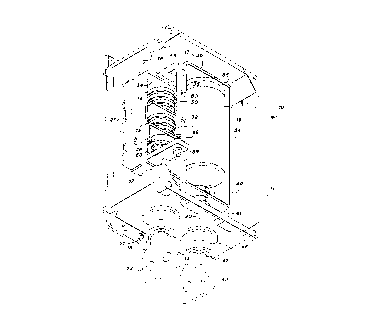
is shown generally at 10 in Fig. 1. The isolation device
l0 includes an enclosure box or casing 11 (which would be
closed with a removable front cover, not shown) within
which are contained electrical components including two
iQ diode stacks 14 and 15,, and a bipolar capacitor 19. The
capacitor 19 preferably has a very large capacitance to
provide low AC impedance, and a relatively high rms current
capability at low voltage. The use of a bipolar capacitor
is preferred so that AC current may be conducted through
the capacitor regardless of the DC bias across the
capacitor and regardless of the instantaneous polarity of
voltage. The two diode stacks 14 and 15 are held in a
clamp assembly 16. The clamp assembly 16 serves to hold
the diode stacks together and to connect them in parallel
with each other as described further below. A first
electrical connection bus 17 provides a connection between
the capacitor 19, the first diode stack 14, and a first
input terminal 18 of the ground isolation device. The
input terminal 18 includes a large flat lug 23 which
extends outwardly from the enclosure 11 and can be
connected to external electrical lines, such as a grounding
strap or wire. The conducting metal of the input lug 23
extends through a bottom wall 20 of the enclosure il (which
may be formed of an insulator such as glass fiber
reinforced polyester or can be a metal cabinet), with an
insulating block 21 preferably used to enclose the
conductor of the lug 23 at its junction_with the bottom
wall 20 of the case. A connecting nut 22 is used to secure
the structure of the input terminal firmly in place on the
bottom wall 20, with an insulator 21 extending up into the
CA 02156209 1999-06-22
_ 7 _
interior of the casing surrounding the conductor 24
_ extending from the lug 23. An electrical connection is
made between the conductor 24 (and thus to the lug 23) and
_ a straight flat section 25 of the conducting bus 17 by a
pair of nuts 26 which are threaded onto the conducting post
24. The nuts 26 are tightened down on the section 25 of
the conductor 17 to provide a tight contact connection.
The nuts 26 are electrical conductors, e.g., brass, and
thus provide a good electrical connection between the
conductors 17 and the input terminal post 24.
The bus bar conductor 17, which is preferably
rigid and formed of a good conducting metal such as copper,
has another straight section 27 which extends upwardly from
the section 25, and to which is joined a,stub section 28,
bolted to the section 27 by a nut and bolt 30, which
includes a straight flat section 32. Thus, the section of
the conductor 32 is in electrical contact with the
conductor 17, and thus with the input terminal 18. The
conductor 17 further has a second straight section 34 which
is spaced above and parallel to the straight section 32.
The conductor 17 further has a section 35 which extends
upwardly from the section 34 and a laterally extending
section 36 which is connected by a bolt 37 to one of the
terminals 38 of the capacitor 19. The bolt 37 not only
provides an electrical connection between the terminal 38
of the capacitor and the section 36 of the conductor 17,
but also a structural connection. Thus, the capacitor 19
is supported physically, in part, by the conductor 17.
A second bus bar conductor 40 has a flat bottom
section 41 which is connected to a second input terminal 42
which is formed in the manner similar to the first input
terminal 18. The second input terminal 42 has a connecting
lug 43 extending outside the enclosure 11, a post 44
extending upwardly therefrom through the bottom wall 20 of
the enclosure, a connecting nut 45 which structurally
connects the input terminal 42 to the bottom wall 20, an
insulator 46 which surrounds the post 44, and two nuts 47
CA 02156209 1999-06-22
- g -
which are threaded onto the post 44 and which are tightened
' down onto the straight conductor section 41 to provide a
good electrical and structural connection between the post
44 and the conductor 40. The second conducting bus bar 40
has an upright section 49 from which extends laterally a
flat section 50 which is spaced intermediate the sections
32 and 34 of the first bus bar conductor and is generally
parallel to the sections 32 and 34. The diode stacks 14
and 15 are mounted between the straight sections 34 and 50
and 32 and 50, respectively, as described further below.
The conductor 40 also has an upright section 54 which
extends upwardly from the right side of the bottom section
41 and a laterally extending section 55 which is
electrically and structurally connected to a second input
terminal 56 of the capacitor 19 by a bolt 57. Because the
conducting bars 17 and 40 are strong, rigid metal
structures, the capacitor 19 is physically supported by its
connection at the input terminals 38 and 56 to the
conducting bars 17 and 40. The connecting conductors 17
and 40 form a rigid structure with large surface areas and
are tightly connected to the electrical components to
minimize connection resistances. These buses are
preferably formed of, e.g., 1/8" thick by about 1 3/4"
wide, copper with a thin (.2 - .5 mm) electroplating of
tin. Conducting buses of this width and thickness provide
very low resistance and good structural rigidity.
The diode stacks 14 and 15 are connected to the
conductor sections 34, 50 and 32 by the clamp assembly 16
so that they are electrically in parallel in opposite
polarity to each other. The clamp assembly 16, as best
illustrated in the views of Figs. 1, 2 and 13, includes a
top brace 58 and a bottom brace 59. Two bolts 16 extend
through openings (not shown) in the top brace 58 and engage
the top face of the top brace 58 with the head 61 of the
bolts 60. The bolts 60 have threads 62 at their bottom
ends, which extend through openings (not shown) in the
bottom brace 59, and nuts 63 are threaded onto the threaded
CA 02156209 1999-06-22
_ g _
portions 62 of the bolts 60 to hold the bottom brace 59 in
place on the bolts 60. A flat metal pressure plate 65 is
mounted between the bottom of the top brace 58 and the
conductor section 34 to transmit pressure evenly from the
brace 58 to the surface of the conducting section 34. A
bottom pressure plate 66 composed of a flat thick disk of
metal is mounted in contact with the bottom conductor
section 32 to apply evenly distributed pressure onto the
surface thereof. Stacks of nested compression washers 67
and 68, extending around a post 69 mounted to the bottom
brace 59, are engaged between the pressure plate 66 and the
bottom brace 59. The number of compression washers used
depends on the clamp pressure needed. The compression
washers 67 and 68 compress to'provide a very stiff spring
action, and as the nuts 63 are tightened down onto the
bolts 60, the brace 59 applies pressure through the washers
67 and 68 to the pressure plate 66 and thence to the
conductor section 32 to apply a large, even pressure to the
diode stacks 14 and l5 and the conductor sections 34, 50
and 32. The use of the compression washers 67 and 68 to
provide a stiff spring allows the pressure applied to the
diode stacks 14 and 15 to be adjusted by tightening the
nuts 63. In addition, pressure will still be applied
between the braces 58 and 59 to the diode stacks 14 and 15
and the conductors 34, 50 and 32 even if the nuts 63 loosen
slightly over time with changes in temperature and
jostling, or if the bolts 60 elongate slightly because of
an increase in temperature or relaxation of the metal of
the bolts. If the compression spring washers 67 and 68
were not used, and the diode stacks were mounted directly
between the braces 58 and 59, a slight loosening of the
nuts 63 or an elongation of the bolts 60 would
substantially or perhaps entirely release the pressure on
the diode stacks.
Although large surface area lugs 23 and 43 are
shown for use in connecting to external conductors, other
forms of terminal connections, such as eye bolt terminals
2156~0~
- 10 -
or insulated flexible leads, may also be used depending on
the specific application. The enclosure 11 may be made of
metal, plastic or composites, such as fiberglass reinforced
polyester, and it completely surrounds the internal
components when a removable or non-removable cover (not
shown) is in place. The space inside the enclosure 11 may
be filled with an encapsulation material to protect the
circuit components from impact damage and also make the
device essentially waterproof. Use of encapsulation would
generally be required for submersible applications of the
device.
The circuit operation of the isolation device is
illustrated with respect to the circuit diagram of Fig. 3.
The isolation device 10 is typically connected between a
structure 70 to be isolated (such as a cathodically
protected pipe) and a ground 71, e.g., a grounding rod.
The device 10 may also be connected between two
cathodically protected structures to provide AC continuity
between the structures. The isolation device circuit
includes the two diode stacks 14 and 15 which are connected
in parallel, and in opposite polarity to each other, across
the conductors 17 and 40, and the bipolar capacitor 19
which is connected in parallel with the diode stacks.
For exemplification, Fig. 3 shows four diodes 75
in series comprising each diode stack 14 and 15. Each
diode 75 in the structure has a forward threshold or cut-in
voltage of about 0.45 volts before it conducts significant
current in the forward direction. Since the capacitor 19
is an open circuit with respect to DC, the circuit shown in
Fig. 3, having four such diodes 75 in series in each of the
stacks 14 and 15, will provide DC current isolation of the
structure to which it is connected up to approximately 1.8
volts DC in either direction. Very low levels of DC
leakage current, 0.1 to 1.0 milliamperes, will typically be
present in practice. At the same time, AC currents will
pass freely through the capacitor. The peak AC voltage
across the capacitor 19 should be less than the threshold
CA 02156209 1999-06-22
- 11 -
voltage across the diode stacks 14 and 15, e.g., 1.8 volts.
_ For example, for a normal AC current of 30 amperes rms at
60Hz being conducted by the capacitor 19 with no DC bias,
- the capacitor should have a capacitance of at least about
70,000 ~cf to maintain the zero to peak voltage across the
capacitor below 1.8 volts with no DC bias. In the presence
of a DC bias on the capacitor, greater capacitance is
required. An exemplary suitable capacitor is a United
Chemi-Con 36DA207*, having a capacitance of about 270,000
~,f. Unipolar capacitors are capable of bipolar operation
provided that the amplitude of the bipolar voltage is small
in relation to the DC voltage rating.
For higher levels of AC currents (or DC
currents), such as that resulting from a system fault, as
the voltage across the capacitor 19 reaches 1.8 volts in
each half cycle one of the diode stacks will be forward
biased and current will be conducted through the diode
stack either to ground 71 or between two structures where
the device is used to provide AC continuity. Thus, the
circuit provides for DC isolation in the presence of low
levels of AC current while providing for effective
grounding of the system in the case of system faults.
Because the diode stacks 14 and 15 limit the voltage which
can appear across the capacitor 19, the capacitor can have
a relatively low voltage rating.
Alternate diode arrangements may also be used for
the electrical isolation device. For example, Fig. 4 shows
the isolation device circuit wherein the diodes have been
arranged in a bridge configuration. This circuit formation
provides the same degree of electrical isolation as the
circuit shown in Fig. 3 but uses two fewer diodes. In this
case four diodes are in series for either polarity. The
bridge is formed across bridge AC terminals 76 and 77,
which are connected to the input terminals 18 and 42, and
bridge DC terminals 78 and 79, with one of the diodes 75A,
75B, 75C and 75D connected in each arm of the bridge. One
or more diodes (two shown, 75E and 75F) are connected
*Trade-mark
r
~1~6 ~~9
- 12
across the DC terminals 78 and 79. Isolation for positive
polarity voltages is provided by the diodes 75A, 75E, 75F,
and 75D. Isolation for negative polarity voltages is
provided by the diodes 75B, 75E, 75F, and 75C. Thus, this
circuit containing six diodes may provide the same degree
of DC isolation as a circuit with eight diodes. However,
in a fault current situation, the diodes 75E and 75F will
be required to pass both polarities of surge current. This
may require a higher rating for these two diodes. This
configuration may also utilize a different arrangement of
diode stacks and electrical conductors than described
above. A single clamp assembly 16 may be used, although
more than two diode stacks may be required, or the diode
stacks may be placed side by side, rather than end to end,
in the clamp assembly 16.
Another alternate diode arrangement for the
isolation device is shown in Fig. 5. In accordance with
this arrangement each diode stack 14 and 15 contains an
unequal number of diodes 75. In an isolation device having
an equal number of diodes 75 in each diode stack 14 and 15
(such as that shown in Figs. 3 or 4) DC bias and cathodic
protection voltage is lost when large AC fault currents are
present. This is because in such a situation each diode
stack will be conducting at the same voltage level on
alternate half cycles and the net DC voltage across the
device, and therefore on the protected structure, will be
0 volts. This is contrasted with the effect of a isolation
device having an unequal number of diodes in each diode
stack. For exemplification, Fig. 5 shows two diodes 75 in
series comprising the diode stack 14 and six diodes 75 in
series comprising the diode stack 15. Each diode 75 in the
structure has a forward threshold or cut-in voltage of
about 0.45 volts before it conducts in the forward
direction. At low AC current the diodes are not conducting,
AC current flows through the capacitor, and DC isolation is
achieved as described above with respect to the symmetrical
isolation device. When large AC fault currents are present
~~ ' ~' 21~~~~
- 13 -
on the isolation device the voltage across the device will
be clamped at the cumulative voltage drop across two diodes
during the positive half cycle of the AC fault current and
at the cumulative voltage drop across six diodes during the
negative half cycle of the AC fault current. Although the
forward voltage blocking level per diode junction is
typically about 0.45 volt for low levels of leakage current
(e. g., 1-10 ma), when the diodes are forced into conduction
from steady state AC power (or AC fault current), the
forward voltage drop across each diode junction typically
will be about 0.75 volt. Thus, with two diode junctions in
one direction and six in the other, the positive peak
voltage will be about 1.5 volts and the negative peak
voltage will be about -4.5 volts. Therefore, the net DC
voltage across the isolation device during periods of AC
fault is about -1.5 volts. This voltage level provides
very acceptable cathodic protection. Moreover, even if the
original applied protection voltage was not at this level,
it will be driven toward this level by the large AC
currents. This is true whether the protection voltage was
originally more negative or more positive then the final
net voltage level achieved.
Conducting paths with unequal numbers of diodes
may also be obtained where a bridge configuration is
utilized, as illustrated in Fig. 4A in which two diodes 75A
and 75AA are connected in series in the same arm of the
bridge.
Thus, by properly selecting an unequal number of
diodes in each diode stack, with the desired threshold
3D voltage, cathodic protection can be maintained even in the
presence of large AC fault currents. A circuit with
unequal numbers of diodes also provides higher DC voltage
blocking in the negative direction, which is preferable,
but as a result is not polarity insensitive and care must
be taken to install the device properly. A non-symmetrical
diode configuration may also allow a reduction in the value
of the capacitance of the capacitor 19. As the value of
., _ ; , ; ~, ~~~ozoo
- 14 -
the capacitance of the capacitor 19 is reduced, more
voltage will appear across the capacitor 19 for a given AC
current. The diodes are thus likely to conduct at a lower
level of AC fault current, or even at high levels of steady
state AC current. However, this is less of a concern with
the asymmetrical diode stack configuration in that when the
diode stacks 14 and 15 are conducting, ideal cathodic
protection voltage may still be maintained. In fact, use
of asymmetrical diode stacks permits the capacitor 19 to be
removed altogether if desired. Such an isolation device
will present a high impedance to both AC and DC until the
breakdown voltage of the diodes is reached. The breakdown
voltages are selected so that high levels of AC current,
steady state or fault, result in a net DC voltage across
the device which is ideal for cathodic protection.
If the capacitor 19 is removed from an
asymmetrical circuit, such as that shown in Fig. 5, the
isolation device may be used to obtain a desired DC
cathodic protection voltage level (approximately -0.70 volt
to -2.50 volts) on a metal structure to which an AC current
is applied (or induced) from an AC source 72. The device
10 may be connected between the structure to be protected
70 and ground 71. When an AC voltage is applied to the
structure 70 such that the AC current causes each diode
stack 14 and 15 to conduct on alternating half cycles, the
result will be a net DC voltage on the structure 70. The
number of diodes, and the threshold voltage of each diode,
in each diode stack can be selected to provide the desired
DC cathodic protection voltage on the structure 70.
As described above, the diode stacks 14 and 15
are preferably connected together and to the electrical
conductors 17 and 40 in a manner which minimizes the total
number of connections required by the system, and the
required connections are made in a manner which minimizes
the connection resistance and inductance. This is
desirable in a circuit of this nature which is intended to
carry very large fault currents. In the presence of such
', . ',
- 15 -
large currents even small resistances or inductances at the
connections between electrical components can result in
large voltage drops.
To reduce connection resistances, it is desirable
that the conducting buses 17 and 40 have large cross-
sectional areas and be capable of direct and simple
connection to the various device components and to the
input terminals 18 and 42. It is preferred that the bus
bar conductors 17 and 40 are connected to the diode stacks
14 and 15, and the components of the diode stacks are
connected to each other, with large area surface contact to
minimize connection resistance in a manner which requires
no intervening connection devices.
Each diode stack 14 and 15, as illustrated in
Figs. 10 and il, is preferably formed of a stack of one or
more diode layers 75, with each layer functioning as a
diode. The diode layers 75 are stacked such that the diode
stack conducts predominantly in only one direction through
the stack when the threshold voltage of the diode stack is
exceeded. The more stack layers 75 which are included, the
higher the turn-on voltage of the stack and the more DC
isolation will be provided by the isolation device.
As illustrated in Fig. 12, the diode stack 14 or
15 may be contained in a polymeric sleeve 83 which holds
the layers 75 together in a stack subassembly. This sleeve
also provides protection of the diode stack from the
environment. The diode stack assembly may also be created
by bonding the layers of the diode stack together, for
example, with solder between the layers, if desired.
At the heart of each diode layer 75 is a diode
junction wafer 85 as shown in Figs. 6-9. Each diode
junction wafer 85 may be the die, or junction only, from a
standard "hockey puck" style power diode. The diode
junction wafers may also be available in special non-
standard sizes. The wafers 85 are two-sided, generally of
silicon, each wafer having an anode (P-doped) side 86 and a
cathode (N-doped) side 87. The joint at the edge of the
- 16 -
wafer between the P-doped and N-doped regions is commonly
protected by a rubber ring 88. Generally there is a metal
disk, such as of molybdenum, alloyed to the silicon and
which thus forms the anode side 86 of the wafer. The
wafers are disk shaped as shown in Fig. 5. Exemplary
suitable wafers are International Rectifier IR24CDR02L (24
mm) and IR38CDR02M (38 mm).
Each diode junction wafer 85 preferably is
combined with one or more additional metal separation disks
to comprise the diode layer 75, as shown in Figs. 8 and 9.
For example, the layer 75 may include a molybdenum disk 90
and a heat sink/spacer disk 91. The molybdenum disk 90 is
placed on the surface 87 of the wafer 85. The molybdenum
disk 90 may or may not be bonded to the diode junction
wafer, as desired. Typical molybdenum disks include
International Rectifier 43-0064-69 (.040" x .070" diameter)
and 43-0064-99 (.020" x 1.213" diameter) or any similar
disks in this size range. This separate disk 90 may also
be made of alternative metals, such as tungsten.
The heat sink and spacer disk 91 is placed on top
of the molybdenum disk 90. The surfaces of the flat
portion of the heat sink disks 91 must be parallel to
assure adequate surface contact when the diode layers 75
are stacked together in the clamp assembly 16 to minimize
connection resistances. A typical heat sink disk will
comprise a 1/8" thick copper disk (though a thicker disk
may be used). The copper disk may be plated in nickel (of
a few microns only) to prevent oxidation of the copper. An
electroless plating process is preferably used because
adequate surface flatness and parallelism might not be
retained with an electroplating process. The surface area
of the disk should not be touched by any plating fixtures
or affected in any way by the plating process. The heat
sink disk may be, but need not be, the same diameter as the
diode junction.
The thickness of the separation disks 90 and heat
sink disks 91 may be adjusted so that isolation devices
215fi~4~
- 17 -
with different ratings may use identical busswork. Since
diodes 75 which have higher current ratings will generally
be thicker, it may thus be desirable to use thinner
separation disks 90 and heat sink disks 91 with such
diodes.
The rating of the isolation device -- the maximum
amount of AC current which it can conduct -- is a function
of the clamp assembly and diode junctions used. For
example, using a diode stack containing four 24 mm diode
junctions clamped to 1200-2000 pounds of clamping pressure,
the isolation device may have a 60 Hz AC symmetrical
current carrying capability for 30 cycles of 3,700 amps
rms. Similarly, an isolation device using diode junction
stacks containing four 38 mm diode junctions clamped at
3500-4000 pounds clamping pressure may have a 60 Hz AC
symmetrical current carrying capability for 30 cycles of
10,000 amps rms.
Operation of the isolation device beyond its
recommended rating may cause the diode junction wafers to
fail. Should a diode junction fail, however, failure will
be in the shorted (low AC/DC impedance) mode. Thus, a
failure will cause a short to ground rather than a
potential shock hazard.
If equal numbers of diode junction stack layers
75 are used in each stack, the isolation device will be bi-
directionally symmetrical. It thus could not be connected
in the wrong direction. As noted above, the isolation
device 10 may also employ diode stacks which do not have
equal number of diode layers 75. The resulting
asymmetrical isolation device will have DC blocking
capabilities of different voltage levels in each direction,
which may be acceptable or even preferable in some
applications. Such a device is, however, no longer
polarity insensitive and the device must be installed in
the proper direction.
It is understood that the invention is not
confined to the particular embodiments set forth herein as
21~~~~~
illustrative, but embraces such modified forms thereof as
come within the scope of the following claims.