Note : Les descriptions sont présentées dans la langue officielle dans laquelle elles ont été soumises.
WO 95/03533 PCT/LTS94/08066
215799
-1-
STATIC PRESSURE COMPENSATION OF
RESONANT INTEGRATED MICROBEAM SENSORS
The present invention relates to transducers that utilize induced strain to
measure
acceleration pressure, temperature and other variables, and more particularly
to
providing temperature and static pressure compensation in such devices.
Resonant transducers have been used for many years to achieve high accuracy
measurements. Vibrating transducers have been used in precision accelerometers
and
pressure sensors. These devices operate on the principle that the natural
frequency of
vibration (i.e. resonant frequency of an oscillating beam or other member) is
a function
of the induced strain along the member. More particularly, tensile forces
elongating the
beam increase its resonant frequency, while forces compressing the beam reduce
the
natural frequency. The frequency output of resonant gages is readily converted
to
digital readings reflecting the measured quantity, requiring only a counter
and a
reference clock for this purpose. Thus, such gages are simple and reliable,
and provide
a high degree of discrimination while using a relatively simple interface to
digital signal
processing circuitry.
One particularly effective transducer of this type is a resonant integrated
microbeam sensor, for example as disclosed in U.S. Patent No. 5,275,055
entitled
"Resonant Gage with Microbeam Driven in Constant Electric Field", and assigned
to the
assignee of this application. The sensor includes a silicon substrate, a
polysilicon
flexure beam attached at both ends to the substrate, and a polysilicon rigid
cover
cooperating with the substrate to enclose the flexure beam within a sealed
vacuum
chamber. A pair of bias electrodes on opposite sides of the beam create a
constant
electrical field about the flexure beam. A drive electrode on the flexure beam
is
selectively charged to oscillate the beam. A piezoresistive element on the
flexure beam
is used to indicate beam position, and also to provide feedback to the drive
oscillator.
Thus, the beam tends to oscillate at its natural resonant frequency.
The sensor can be fabricated on a pressure sensor diaphragm or a flexure of an
accelerometer, to be elongated or compressed by deflections of the diaphragm
or flexure
in response to pressure changes and accelerations, respectively. While
satisfactory in
many of these applications, the sensors are subject to error due to deviations
in
temperature and in static pressure.
WO 95/03533 1 5 7 ~ ~ 9 ~ PCT/US94/08066
-2-
It is known, in connection with resonant sensors, to provide compensation for
variations in temperatures and other conditions. For example, U.S. Patent No.
4,535,638 (EerNisse et al) discloses a resonator transducer system in which a
vibratory
element such as a quartz crystal is driven to oscillate at two frequencies,
both of which
S vary with changes in applied force and changes in temperature. The frequency
outputs
are processed by a computer containing predetermined coefficients for
correcting as to
the temperature effect.
U.S. Patent No. 4, 598,381 (Gucci) discloses a pressure compensated
differential
pressure sensor. A reference sensor senses a relatively low reference
pressure, and a
second sensor senses a differential between the lower pressure and a higher
second
pressure. Outputs of the pressure sensors and a temperature sensor are
provided to a
computer, programmed to correct for temperature effects. The computer includes
an
analog to digital converter receiving the temperature sensor output.
In U.S. Patent No. 4,765,188 (Krechmery et al.), a pressure transducer
includes a
diaphragm with several piezoresistor strain gages for sensing pressure. A
temperature
dependant resistor also is formed on the diaphragm. The output of the
temperature
sensitive resistor is converted to a digital signal provided to a programmable
read only
memory (PROM). The PROM stores correction data to provide temperature
compensation.
While the above approaches are workable, they require storage of compensation
data, and frequently require analog to digital conversion, adding on to
complexity of
sensing and compensation circuitry and thus increasing the difficulty of
semiconductor
device fabrication.
Therefore, it is an object of the present invention to provide a resonant
sensing
device in which sensors provided for compensation generate digital outputs,
eliminating
the need for analog to digital signal conversion.
Another object is to provide, in a single measuring device, the combination of
a
primary resonant sensor and at least one secondary resonant sensor for
compensation.
Yet another object is to provide a measuring device in which one or more
secondary resonant sensors used for compensation are substantially identical
in size and
internal strain, to provide for simple and reliable compensation that does not
require
storage of multiple compensation values in computer memory.
WO 95!03533 PCT/US94/08066
2157909_
-3-
To achieve these and other objects, there is provided a parameter measuring
device. The device includes a semiconductor substrate having a substantially
rigid first
region, and a second region substantially more flexible than the first region.
An
elongate primary vibratory element has opposite first and second end portions
fixed with
respect to the second region, for longitudinal extension and compression of
the vibratory
flexure element responsive to flexure of the second region. The device further
includes
an elongate secondary vibratory element fixed with respect to the first
region, having a
natural resonant frequency that varies responsive to changes in a secondary
parameter
but is substantially unaffected by changes in the primary parameter.
The primary vibratory element responds by an increase in its natural resonant
frequency with vibratory element elongation, and a decrease as the element
either
contracts or is compressed. The primary vibratory element responds to
fluctuations in
the primary parameter and in the secondary parameter, while the secondary
vibratory
element responds only to fluctuations in the secondary parameter.
Each of the primary and secondary vibratory elements is driven at its resonant
frequency by an associated means for generating a substantially uniform and
constant
electrical field in the region of the vibratory element, a position sensing
means for
sensing the position of the vibratory element relative to the substrate, and
an oscillating
means for generating a periodic drive voltage signal responsive to changes in
the
vibratory element position. The drive voltage signal causes a periodic
mechanical
oscillation of the vibratory element relative to the substrate. The
oscillating means
continually and controllably adjusts the drive signal frequency in response to
variations
in the position signal frequency, thereby adjusting the drive signal toward
coincidence
with a natural resonant frequency of the mechanical oscillation.
The measuring device further includes signal processing means for receiving
the
resonant frequency outputs of the primary and secondary vibratory elements,
and for
compensating the primary vibratory element by combining it with the secondary
vibratory element output in a manner to extract the portion of the frequency
dependant
on fluctuations in the secondary parameter. The result is a frequency output
dependent
only upon the primary measured parameter.
PCT/US94108066
WO 95/03533
-4-
In one particularly preferred embodiment, the primary and secondary vibratory
element are substantially identical in size, material and residual strain. In
that event, the
secondary output is used as a reference frequency, and the ratio of the square
of the
primary frequency to the square of the secondary frequency varies with applied
strain
according to the following formula:
f2
p =a+be
f2
s
where fp is the primary frequency, fs is the secondary or reference frequency,
s is
applied strain (to the primary flexure member), and a and b are constants.
Accordingly,
by measuring fp and fs at two different values of the primary parameter while
maintaining the secondary parameter constant (for example, measuring at two
different
pressures while maintaining temperature), the constants a and b can be
determined.
Once determined, these constants yield a compensated value of the primary
parameter,
based on strain applied to the primary flexure member as determined by the
resonant
frequency of the primary flexure member.
The primary and secondary parameters being measured play a key role in the
positioning of the primary and secondary flexure beams. For example, in a
pressure
transducing device including a semiconductor chip with a diaphragm mounted
atop a
tube of Pyrex glass or similar material, the diaphragm provides the more
flexible second
substrate region, and a rigid rim surrounding the diaphragm and mounted to the
tube
provides the more rigid first substrate region. The preferred location for the
primary
vibratory element is at the diaphragm periphery, either perpendicular to the
edge of a
rectangular diaphragm or radial relative to a circular diaphragm. The
secondary
vibratory element, e.g. a temperature sensing microbeam, is preferably
positioned near
the periphery of the chip, beyond the Pyrex tube. A further secondary
vibratory
element, a static pressure sensing microbeam, can be positioned along the chip
periphery where the static pressure effects are likely to be largest.
Alternatively, a
second diaphragm smaller than the differential pressure sensing diaphragm can
be
fabricated into the chip for use with a static pressure sensor.
Finite element models of the chip are advantageously used in determining
appropriate vibratory element positions. Such models can be based on
differential
CA 02157909 2005-02-14
64159-1428
. _5_
pressure in the range about 15 psi, or can be based on
static pressure in the range of about 1000 psi. Thus, in
accordance with the present invention there is provided a
simple and reliable means for employing a resonant microbeam
to sense differential pressures and accelerations,
substantially free of temperature and static pressure
effects.
In accordance with one aspect of this invention,
there is provided a sensing device including: a substrate
having a substantially rigid first region and a second
region more flexible than the first region, the second
region flexing in response to variations in a first
parameter; an elongate primary vibratory element having
opposite first and second end portions fixed with respect to
the substrate to position the primary vibratory element
along the second region, for lengthwise extension and
contraction of the primary vibratory element responsive to
the flexing of the second region, said extension and
contraction varying a primary natural resonant frequency of
the primary vibratory element, the primary natural resonant
frequency being varied in response to changes of the first
parameter and a second parameter; an elongate secondary
vibratory element fixed with respect to the substrate, said
secondary vibratory element having a secondary natural
resonant frequency variable in response to changes in the
second parameter, while substantially unaffected by
variations in the first parameter; means for sensing the
primary and secondary resonant frequencies and for
generating an output representing the primary parameter
compensated for the effect of the secondary parameter, based
on said primary and secondary natural resonant frequencies.
In accordance with another aspect of this
invention, there is provided a measuring device, including:
CA 021157909 2005-02-14
64159-1428
-5a-
a substrate having a flexible diaphragm that flexes in
response to variations in a first parameter, and a
substantially rigid peripheral region surrounding and
supporting the diaphragm; an elongate primary vibratory
element having opposite first and second end portions fixed
to the substrate along one side of the flexible diaphragm
near said peripheral region, for lengthwise extension and
contraction of the primary vibratory element responsive to
the flexing of the diaphragm, said extension and contraction
varying a primary natural resonant frequency of the primary
vibratory element; an elongate secondary vibratory element
fixed with respect to the substrate and having a secondary
natural resonant frequency that varies with a secondary
parameter; means for sensing and indicating the primary and
secondary natural resonant frequencies; and means for
storing two calibration constants "a" and "b", for relating
the primary and secondary natural resonant frequencies
according to the following equation:
fz
-' - a + be
fz
z
where fl is the primary natural resonant frequency, f2 is the
secondary natural resonant frequency and a is the strain
applied to the primary vibratory element.
In accordance with yet another aspect of this
invention, there is provided a sensing device including: a
semiconductor substrate; an elongate primary vibratory
element formed of a semiconductor material and fixed with
respect to the substrate to oscillate at a primary natural
resonant frequency that varies with changes in a first
variable condition, and with changes in a second variable
condition; an elongate secondary vibratory element formed of
a semiconductor material and fixed to the substrate to
CA 021157909 2005-02-14
64159-1428
-5b-
oscillate at a secondary natural resonant frequency that
varies responsive to changes in said second variable
condition but not to changes in said first variable
condition; primary resonant frequency sensing means for
sensing the primary natural resonant frequency and
generating a primary frequency signal based on the primary
resonant frequency; secondary frequency sensing means for
sensing the secondary natural resonant frequency and for
generating a secondary frequency signal based on the
secondary resonant frequency; means for receiving the
primary and secondary frequency signals and forming a ratio
of the square of the primary natural resonant frequency to
the square of the secondary natural resonant frequency;
means for generating an output representing the first
variable condition compensated for the effect of the second
variable condition, based on the ratio of the squares of the
primary and secondary natural resonant frequencies.
In accordance with a further aspect of this
invention, there is provided a process for calibrating
multiple strain responsive resonant beams on multiple chips
of a semiconductor wafer, wherein all of the resonant beams
to be calibrated are substantially uniform in size and
residual stress, wherein the resonant beams include multiple
primary resonant beams, each primary resonant beam having a
primary resonant frequency that varies responsive to changes
in a first variable condition and to changes in a second
variable condition; wherein the resonant beams further
comprise multiple secondary resonant beams, each having a
secondary resonant frequency that varies responsive to
changes in the second variable condition but not to changes
in the first variable condition; wherein each of the
multiple chips includes at least one of the primary resonant
beams and at least one of the secondary resonant beams; said
CA 02157909 2005-02-14
64159-1428
-5c-
process including the steps of: subjecting a selected one of
the semiconductor chips to a first level of the first
~ variable condition and to a first level of the second
variable condition, while concurrently measuring the
respective resonant frequencies of a selected one of the
primary resonant beams and a selected one of the secondary
resonant beams, to provide a first frequency value
representing the resonant frequency of the selected primary
resonant beam and a second frequency value representing the
resonant frequency of the selected secondary resonant beam;
applying a second level of the primary variable condition
and the first level of the secondary variable condition to
the selected semiconductor chip while concurrently measuring
the respective resonant frequencies of the selected primary
and secondary resonant beams, to provide a third frequency
value representing the frequency of the selected primary
resonant beam and a fourth frequency value representing the
natural resonant frequency of the secondary resonant beam;
and utilizing the first, second, third and fourth frequency
values to solve for two constants "a" and "b" of the
equation:
f2
J-' - a + b~
fz
z
where fl is the natural resonant frequency of the primary
resonant beam, fz is the natural resonant frequency of the
secondary resonant beam, and E is the strain applied to the
primary resonant beam.
CA 02157909 2005-02-14
64159-1428
-5d-
For a further understanding of the above and other features and advantages,
reference is made to the detailed description and to the .drawings, in which:
Figure 1 is as elevational sectional view of a pressure sensing device
constructed
in accordance with the present invention;
Figure 2 is a top plan view of the a sensing device;
Figure 3 is an enlarged partial sectional view showing part of Figure 1;
Figure 4 is a sectional view taken along the line 4-4 in Figure 3;
Figure 5 is a schematic view of a resonaat gage and associated oscillator
circuit
of the device;
Figures 6-8 are top plan views of different alternative pie sensing devices
constructed according to the present invention;
Figures 9 aad 10 illustrate finite element models of a pressure sensitive
semiconductor substrate employed in the pressurt sensing devices;
~ Figure 11 schematically illustrates a signal processing system -for a
pressure
sensing device employing four resonant microbeam sensors;
Figure 12 is a top plan view of an accelerometer consst<uuctad according to
the
presentinvention;
Figure 13 is an enlarged sectional view of the accelerometer, taken along the
line
13-13 in Figure 12;
Figure 14 is a sectional view of a the accelerometer taken along the line 14-
14 in
Figure 13.
Turning now to the drawings, there is shown in Figures 1 and 2 a presstnr
sensing device 16. The device includes a silicon substrate or base 18
including a
substantially rigid peripheral region or rim 20 and a diaphragm 22 surrounded
by the
rim. The diaphragm is substantially square, with each side being in the range
of about
4-150 mils in length. The diaphragm is flexible and thin, e.g. having a
thickness in the
WO 95/03533 ~ ~~ ~ ~ PCT/US94108066
-6-
range of 10-100 micrometers. The diaphragm thus provides a substrate region
substantially more flexible than the peripheral region. The bottom of
peripheral rim 20
is thermoelectrically bonded to a tube 24 of Pyrex (brand) glass or other
suitable
material, e.g. ceramics, mullites, certain plastics or silicon. Tube 24 is
supported within
rigid structure at 26. A cover 28 is fastened to the support structure, and
cooperates
with the structure to define a chamber 30. Thus, sensing device 16 is
positioned at the
interface of chamber 30 and the interior of tube 24.
A pressure responsive resonant strain gage 32 is fabricated on the top of
sensing
device 16, to diaphragm 22 near the peripheral region 20. A substantially
similar
resonant gage 34 is mounted to the sensing device at peripheral region 20, in
particular
within the projection of the annular face of tube 24. Resonant gage 34 is
selectively
oriented with respect to tube 24, i.e. perpendicular to the tube radius, to
minimize static
pressure effects. Accordingly, resonant gage 34 does not respond to flexure of
the
diaphragm. Gage 34 thus is used as a reference, for compensating for movements
of
1 S gage 32 in response to changes in temperature rather than to pressure
induced
diaphragm flexure. While diaphragm 22 is square as shown in Figure 2, the
diaphragm
can be formed with an alternative shape, e.g. circular or rectangular, if
desired.
Anisotropic etching is employed to form rectangular or square diaphragms,
while
isotropic etching techniques can be employed to form a circular diaphragm.
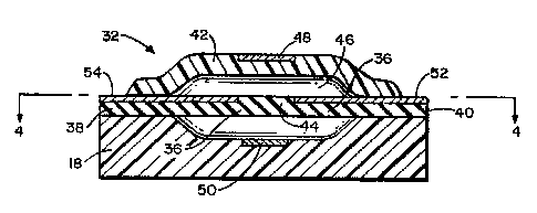
As seen in Figure 3, resonant gage 32 includes an elongate beam 36 formed of
fine grain, low tensile strain polysilicon (polycrystalline silicon). Beam 36
has a length
in the range of 50-1000 micrometers and more preferably about 200 micrometers,
a
thickness (vertical in Figure 3) of about 1-3 micrometers, and a width of
about 20-80
micrometers. Opposite ends of the beam, indicated at 38 and 40, are fixed
between
substrate 18 (more particularly the diaphragm) and a substantially rigid shell
or cover
42, also formed of polysilicon. A medial region 44 of the beam is free to
oscillate
within a chamber 46 formed by the cover and the substrate.
An upper bias electrode 48 is formed (e:g. by ion implantation) into a surface
portion of cover 42, and a similar lower bias electrode 50 is formed into a
surface of
diaphragm 22 along the bottom of chamber 46. A drive electrode 52 is formed
along a
portion of the top surface of beam 36. A piezoresistor 54 is formed along the
top
surface of the beam and is co-planar with drive electrode 52, spaced apart
from
~15790~ .
_7_
electrode 52 and therefore electrically isolated from the drive electrode.
Electrodes 48
and 50 are spaced apart from drive electrode 52 transversely with respect to
the length
or longitudinal dimension of the beam. Drive electrode 52 is approximately
transversely
centered between the bias electrodes.
As seen in Figure 4, beam 36 is formed as part of a larger polysilicon thin
film 56,
with longitudinal gaps 58 and 60 extended along opposite sides of the beam.
Drive
electrode 52 is substantially rectangular, although the shape is not critical.
Piezoresistor
54 includes contact regions 62 and 64 and a relatively thin pair of legs 66
and 68. The
legs extend into the beam medial region from the pads to an enlarged portion
70 that
electrically couples the legs. The electrical impedance of the legs is
substantially greater
than that of enlarged portion 70. Thus, virtually all of the voltage
differential between
pads 62 and 64 occurs across the legs. This promotes maintaining enlarged
portion 70 at
a desired voltage level.
Pressure sensing device 16 measures a pressure differential (i.e. the
difference
between pressures P 1 and P2 on opposite sides of diaphragm 22), based on the
frequency at which beam 36 oscillates. More particularly, when diaphragm 22
flexes in
response to differing pressures P1 and P2, it produces axial or longitudinal
stress upon
beam 36, altering the strain along the beam. Downward diaphragm flexure tends
to
elongate beam 36 and increase its natural frequency. Conversely, upward
diaphragm
deflection tends to allow beam contraction or compress the beam, thus to
reduce its
resonant frequency.
To maintain the required oscillation of the beam, a periodically oscillating
voltage
level is provided to drive electrode 52, while a substantially uniform
constant electrical
field is maintained in the region about the beam. For a more detailed
explanation of
beam oscillation see the aforementioned U.S. Patent No. 5,275,055.
Piezoresistor 54
fi~nctions as a means for detecting the instantaneous position of beam 36
relative to the
substrate and cover 42, by generating a detector voltage that varies with the
beam
position.
The detector voltage is provided as an input to an oscillator circuit, the
output of
which is the periodic drive voltage signal. The drive voltage signal is
provided to drive
electrode 52, to maintain beam 36 in steady state oscillation at its natural
resonant
frequency. For a polysilicon beam of the microscopic size described, the
resonant
Af~AENDED SIT
'~.. ~~c.. ut4 ix ~ . .
. . _ _ _ .
y
WO 95103533 ~ ~ ~ ~ ~ PCT/LTS94/08066
_g_
frequency tends to be in the range of 200-500 kHz. The oscillator circuit,
shown
schematically at 72 in Figure 5, provides a closed loop for continually
adjusting the
frequency of the drive signal toward coincidence with the natural resonant
frequency of
beam 36. Bias electrodes 48 and 50 are biased at levels +V and -V,
respectively, to
generate a uniform and constant electric field in the region about beam 36,
and more
particularly about drive electrode 52. Resistances 74 and 76 are approximately
equal in
value, to bias the drive electrode at ground. As beam 36 mechanically
oscillates,
piezoresistor 54 provides the detector signal as an input to an amplifier 78
of the
oscillator circuit. The detector signal is a voltage that oscillates at the
same frequency
as the frequency of beam oscillation. An automatic gain control circuit 80
provides
feedback to amplifier 78, to prevent distortion at the oscillation frequency.
The drive
voltage signal, provided to drive electrode 52, is based upon the output of
amplifier 78.
The oscillator circuit includes diodes (not shown) to clamp the signal
amplitude, thus to
limit beam oscillation to within the linear response range. Other means of
amplitude
control, well known in the art, can be used to maintain the drive amplitude.
The output of amplifier 78 is provided to an output buffer amplifier 82. The
output of the buffer amplifier is provided to a digital counter 84 controlled
by a clock
oscillator 86. The output of counter 84 is provided to digital circuitry (not
shown) for a
direct, real-time reading of strain, pressure, or other parameter that
influences the
resonant frequency of beam 36 as it oscillates.
As noted above, changes in strain along the length of beam 36, in response to
longitudinally applied external forces, alter the natural resonant frequency
of the beam.
As the beam begins to oscillate at a different frequency in response to a
change in strain,
the different frequency is sensed in piezoresistor 54, and the detector signal
is provided
to amplifier 78 at the new frequency. The output of amplifier 78 controls the
frequency
of the drive voltage signal. Thus, the drive voltage signal frequency is
continually and
controllably adjusted toward coincidence with the natural resonant frequency
of the
beam. In practice, changes in resonant frequency as compared to a natural base
frequency (Of/f) have been found to be at least six hundred times and up to
1,500 times
the changes in strain or beam elongation (01/1). This provides a high degree
of accuracy
and sensitivity to slight changes in strain. By comparison, a conventional
single crystal
silicon piezoresistor typically has a gauge factor in the range of about sixty
to one
WO 95103533 ~ ~ ~ ~ ~ ~ ~ PCT/US94/08066
-9-
hundred. This gauge factor is measured in terms of resistance (OR/R) compared
to
strain (~l/1).
For more detail as to the oscillator circuit and a method of fabricating the
substrate and resonant gauges, reference is made to the aforementioned U.S.
Patent No.
5,275,055.
Returning to Figure 2, it is to be appreciated that resonant gauge 34 is
substantially identical in construction to resonant gauge 32, particularly in
that gauge 34
has an elongated flexure element or beam substantially the same size as beam
36, and
also formed of fine grain, low tensile strain polysilicon. The utility of
resonant gauge
34 depends on its positioning on pressure sensing device 16. More
particularly,
resonant gauge 34 can be positioned to compensate for temperature induced
error in
resonant beam 36. Differential pressure is the primary parameter monitored by
the
device, and changes in the differential pressure dominate changes in beam
strain. The
beam, however, also is influenced by changes in secondary parameters or
conditions,
e.g. temperature, which can change the density and elastic modulus of the
beam.
Accordingly, strain gauge 34 is provided for temperature compensation, to
eliminate or minimize errors in the resonant frequency output caused by
changes in
temperature. For optimum temperature compensation, resonant gauge 34 is
located on
rim 20, remote from diaphragm 22. This location is essentially free from the
effects of
differential pressure (diaphragm flexure) and changes in static pressure
(substrate
flexure). Thus, the detector voltage output of resonant gauge 32 is influenced
by
temperature and the flexing of diaphragm 22, while the detector voltage output
of
resonant gauge 34 is affected only by temperature. Each of the detector
voltages can be
provided to a counter, with the respective counter outputs processed to
determine a
compensated differential pressure, virtually free of error due to temperature
effects.
The result is substantially improved accuracy in differential pressure
measurements. Because resonant gauges 32 and 34 are substantially the same,
the
substrate and beam elements can be formed monolithically, minimizing
mechanical and
thermal hysteresis, and substrates supporting two or more resonant gauges lend
themselves to batch fabrication.
Figure 6 illustrates an alternative sensing device 90 including a rectangular
substrate 92 thermoelectrically bonded to a support indicated in broken lines
at 94.
WO 95/03533 ~ ~ ~ PCTILJS94108066
-10-
Further broken lines at 96 indicate a rectangular diaphragm substantially
centered within
substrate 92. A primary resonant strain gauge 98 is mounted along a peripheral
edge of
diaphragm 96, much in the same manner as gauge 32. A secondary, temperature
compensating resonant strain gauge 100 is fabricated on a rigid region of the
substrate,
in particular at a corner of the substrate remote from the diaphragm.
Resonant strain gages are further subject to error due to changes in static
pressures. While differential pressures are typically on the order of 15 psi,
the static
pressures can be substantially higher, e.g. about 2,000 psi. Pressures of this
magnitude
are sufficient to elastically deform the relatively rigid regions of the
substrate.
To compensate for static pressure effects, Figure 7 illustrates a differential
pressure sensing device 102 including a rectangular substrate 104 mounted on a
Pyrex
tube, indicated by broken lines at 106. Further broken lines indicate the
location of a
rectangular diaphragm formed in the substrate. A primary resonant strain gauge
110 is
positioned along a peripheral edge of the diaphragm. A secondary resonant
strain gauge
112 is located on the substrate, directly over the face of tube 106, remote
from the
diaphragm. The resonant gauge can be radially oriented as shown, or
tangential. In
either event, the location is chosen for the high stresses due to static
pressure.
Figure 8 illustrates an alternative differential pressure sensing device 114
in
which a rectangular semi-conductor substrate 116 having a central primary
diaphragm
118 is thermoelectrically bonded to a Pyrex tube shown in broken lines at 120.
A
primary resonant strain gauge 122 is mounted along a peripheral edge of the
diaphragm.
A secondary diaphragm 124, smaller than primary diaphragm 118, is fabricated
in an
otherwise substantially rigid substrate region. A secondary resonant strain
gauge 126 is
positioned along a peripheral edge of the secondary diaphragm. The secondary
diaphragm is part of a sealed cavity which provides a reference pressure.
Providing the
secondary diaphragm dedicated to static pressure measurement is preferred when
greater
sensitivity is required.
Figures 9 and 10 illustrate finite element models of substrate 18 when
subjected
to a vertically applied load differential of 15 psi, and a static pressure
load of 1,000 psi,
respectively. As seen in Figure 9, maximum diaphragm stresses occur near the
periphery, particularly near the mid-portion of each side of the diaphragm.
Accordingly,
WO 95/03533 PCT/US94/08066
-11-
optimal placement of the primary resonant strain gauge is as illustrated in
Figures 2 and
6-8.
As seen in Figure 10, the substrate undergoes deflection when subject to
static
pressure. Secondary resonant strain gauges for temperature compensation are
preferably
S placed outwardly, beyond the point of attachment to the tube. Conversely,
secondary
resonant strain gauges for static pressure compensation should be placed in
alignment
with the annular area of attachment to the Pyrex tube, where there is a
maximum change
in strain due to static pressure.
Returning to Figure 8, a further primary resonant strain gauge 128 is mounted
to
substrate 116 at the center of diaphragm 118. Gauge 128, like strain gauge
122, is
intended to measure differential pressure. Considering resonant gauges 122 and
128 in
view of the finite element model in Figure 9, it is apparent that a downward
deflection
of diaphragm 10 (P 1 greater than P2) tends to elongate the beam of resonant
gauge 122,
while compressing the beam of resonant gauge 128. Conversely, upward
deflection of
the diaphragm compresses the beam of gauge 122 and elongates the beam of gauge
128.
The respective resonant frequency signal outputs of resonant gauges 122 and
128 are
subtracted, resulting in a representative output at about twice the signal
amplitude of
each resonant gauge considered alone, for enhanced accuracy. An additional
benefit is
that first order non-linear effects, a source of possible error particularly
at low
differential pressures, substantially cancel one another.
Figure 11 schematically illustrates a signal processing system 130 for
generating
an output that accurately depicts differential pressure, based on temperature
compensation and static pressure compensation. The system includes four
oscillator
circuits at 132, 134, 136 and 138. The oscillators generate voltage outputs
representing
the respective natural resonant frequencies of: a primary resonant gauge
centrally
positioned on the substrate diaphragm; a primary resonant gauge positioned at
the
diaphragm periphery; a secondary temperature compensating gauge positioned at
a
peripheral edge of the substrate; and a secondary static pressure compensation
resonant
gauge aligned with a point of substrate attachment to a Pyrex glass tube.
Digital counters at 140, 142, 144 and 146 receive the respective oscillator
outputs, generate respective counts and provide the respective counts to a
microprocessor 148. Other well-known means for determining frequencies can be
WO 95/03533 PCT/US94/08066
i~~~ _12_
employed. Within the microprocessor, the counts associated with the primary
resonant
gauges are subtracted, and the resonant frequency outputs of the secondary
resonant
gauges are processed according to parameters pre-stored in the micro
processor, e.g. in a
programmable read only memory (PROM), in a known manner. Accordingly,
processor
148 provides as its output a precise reading of differential pressure,
virtually unaffected
by changes in temperature and static pressure.
Alternatively, for temperature compensation, the programming necessary in
microprocessor 148 can be simplified considerably by fabricating the primary
resonant
strain gauge and secondary resonant strain gauge substantially identically, so
that the
respective flexure beams are the same size, same material and have the same
internal
strain in the absence of an applied load. This is because the square of the
resonant
frequency of a resonant microbeam can be closely approximated using the
following
equation:
f2 _ 42E42 ~1+2L2 (s+so)~
pL 7h
where E is the modulus of elasticity, rho(p) is the density, h is the beam
thickness, L is
the beam length, Epsilon (s) is the strain caused by the sensed variable (e.g.
diaphragm
deflection due to differential pressure) and sp is the residual strain.
Assuming that the
residual strain is independent of temperature, a reasonable assumption for
fine grain
polysilicon beams, the frequency is given by:
f=g(T)a(1 +bsp+bs)
where g equals E/p and depends on temperature. The values a and b are
constants that
depend on geometry only. Then, the ratio of sensing frequency fp (primary
gauge) to
reference frequency fs (secondary gauge) is:
f2
p =a+bs
f2
s
This enables the frequency squared ratio to be determined, based upon the
constants a
and b, in combination with the applied strain s. Thus, calibration is a matter
of
determining the constants a and b, and can be accomplished by taking
respective
~1~'~~~~
WO 95/03533 PCT/US94/08066
-13-
frequency readings at two different pressure readings at the same temperature.
Microprocessor 148 is required to store only the calibration constants a and
b, rather
than a series of values over a wide range of resonant frequency readings.
This phenomenon enables a convenient calibration means for multiple
S microbeams fabricated on a single semiconductor wafer where beam dimensions
are
substantially uniform, as are the internal strain values of each micro beam.
In particular,
the constants a and b calibrated for one of the beams are assumed to apply to
all beams
of the semiconductor wafer.
For example, assume a semiconductor wafer is comprised of multiple
semiconductor chips, each chip including either a circular or rectangular
diaphragm
surrounded by a more rigid peripheral region. Assume further that each chip
includes at
least one strain gage mounted on the diaphragm for responding to differential
pressure,
and at least one secondary microbeam strain gage mounted to the peripheral
region and
responsive to changes in temperature. Of course, the primary strain gage also
responds
1 S to changes in temperature for low precision sensing applications.
Calibration of the
semiconductor chips can proceed as follows.
First, a selected one of the semiconductor chips is exposed to a first level
of
differential pressure at a given temperature. Respective natural resonant
frequency
measurements are taken, for the primary resonant beam and for the secondary
resonant
beam. Next, the selected semiconductor chip is exposed to a different level of
differential pressure, at the same temperature. Again, the natural resonant
frequencies
of the primary and secondary resonant beams are measured.
Then, the values obtained for natural resonant frequencies are applied to the
equation provided immediately above, to solve for the constants "a" and "b".
Once
obtained in this manner, the constants a and b are retained for future
reference in
calculating the applied strain epsilon (s), based on the respective measured
natural
resonant frequencies of the primary and secondary resonant beams. The
constants a and
b can be applied not only to the selected chip, but to all other semiconductor
chips of the
semiconductor wafer, because all of the resonant beams subject to calibration
have been
fabricated to be substantially uniform in size and residual stress.
Figures 12-14 illustrate an accelerometer 150 fabricated of semiconductor
material. The accelerometer includes a first substrate layer 152 preferably
formed of
PCTIUS94108066
WO 95103533
-14-
silicon, a second substrate layer 154 including a proof mass; and a third
substrate
capping layer 156. Together, these layers provide a relatively rigid
peripheral rim 158.
A secondary resonant strain gauge 160, for temperature compensation, is
fabricated in
polysilicon layer 154 along the rim and beyond cover layer 156.
As best seen in Figure 14, semiconductor substrate layer 154 includes a proof
mass 162, supported relative to peripheral rim 158 by eight narrow bridges or
flexures,
two of which are indicated at 164 and 166. Between each pair of adjacent
bridges, there
is a gap between the proof mass and the peripheral rim. Several of these gaps
are
indicated at 168. As seen in Figure 13, each of bridges 164 and 166 consists
of upper
and lower narrowed regions formed in semiconductor substrate layer 154. These
narrowed regions flex to allow displacement of proof mass 162 relative to
substrate 152
and cover 156, vertically as viewed in Figure 13. Such displacement of the
proof mass
occurs when the accelerometer is subject to accelerations.
Accelerometer 150 includes two primary resonant strain gauges 170 and 172,
one fabricated onto substrate layer 154 at each of bridges 164 and 166. Each
primary
resonant gauge includes a resonant microbeam, supported at both ends and
subject to
induced strain from flexure of its associated bridge during accelerations and
decelerations.
The primary resonant strain gauges are selectively positioned for a cumulative
response. More particularly, resonant gauge 170 is mounted toward an outward
or
peripheral edge region of its associated bridge 164. By contrast, resonant
gauge 172 is
mounted proximate an inward edge region of bridge 166. Consequently, an
acceleration
induces compressive strain on one of the resonant gauges while simultaneously
inducing
tensile strain upon the other gauge. For example, whenever accelerometer _150
is
subject to an upward acceleration (as viewed in Figure 13), proof mass 162
tends to lag
relative to the remainder of the accelerometer. In other words, the proof mass
is
displaced downwardly relative to cover 156 and substrate 152. This downward
movement tends to elongate the upper narrowed region of bridge 164 near
resonant
gauge 170 while tending to shorten the upper narrowed region of bridge 166
near
resonant gauge 172. The respective resonant frequency signal outputs of
resonant
gauges 170 and 172 are subtracted, resulting in a representative output at
about twice
the signal amplitude of each resonant gauge alone, for enhanced accuracy. A
further
WO 95/03533 ~ ~ '~ (~ ~ ~ PCT/US94/08066
-15-
advantage is that first order non-linear effects, a source of possible error
particularly at
low accelerations, substantially cancel one another.
Secondary resonant strain gauge 160 is fabricated onto the accelerometer along
the peripheral rim, remote from proof mass 162 and the bridges. At this
location,
secondary resonant gauge 160 remains subject to induced strain due to
temperature
effects. At the same time, secondary gauge 160 is virtually free of effects
due to
accelerations, in particular free of induced strain due to bridge flexure.
Accordingly, an
output detector voltage of the secondary resonant gauge can be combined with
the
detector output voltages of primary resonant gauges 170 and 172, to yield an
output
compensated for temperature effects. It is to be appreciated that secondary
resonant
gauge 160 can be fabricated onto proof mass 162 at a point remote from the
bridges, if
desired. Also, oscillator circuits associated with the primary resonant gauges
and the
secondary gauge, while not illustrated, can be substantially as described
above in
connection with the differential pressure sensing devices.
Thus, in accordance with the present invention, two or more resonant micro
beam sensors can be fabricated monolithically on a semiconductor substrate,
and used in
concert to provide enhanced accuracy in measuring a primary condition or
parameter,
e.g. differential pressure or acceleration. Precision is enhanced by
positioning one or
more secondary resonant microbeam sensors, in a manner that each sensor
responds
only to a secondary parameter or condition, e.g. temperature or static
pressure. In each
case, the location of the primary or secondary sensor is determined based on
finite
element modeling of the substrate to determine the nature of its response to
one or more
of the parameters. If a temperature compensation microbeam has the same size,
construction and internal strain as the primary resonant microbeam, a simple
calibration
involving two constants can be employed in lieu of storing multiple
compensation
values in a PROM or other computer memory. Further, in connection with
temperature
compensation, a cantilevered mounting of the temperature compensation
microbeam
eliminates the need for critically positioning the sensor.