Note : Les descriptions sont présentées dans la langue officielle dans laquelle elles ont été soumises.
216~2~
-
EASILY PROGRAMMARTT~ MEMORY CONTROLLER
WHICH CAN ACCESS DIFFERENT SPEED MEMORY
DEVICES ON DIFFERENT CYCLES
The invention relates to memory controllers
utilized in computer systems, and more particularly to
a memory controller which can operate with different
speed memory devices in separate banks and additionally
with different speed microprocessors.
Computer systems are becoming ever more powerful
by the day. Users are requiring more capabilities to
run ever more complicated and sophisticated
applications and computer system manufacturers are
responding. Computer speeds have dramatically
increased over the last number of years so that now
desktop and file server computers can readily
outperform mainframe computers of 10-15 years ago. But
the quest for further performance is never ending. To
this end, the microprocessor manufacturers have been
developing ever faster microprocessors.
However, a computer system is far more than just a
microprocessor. There are many other subsystems that
must cooperate with the microprocessor to provide a
complete computer system. It is desireable to optimize
2160200
-
as many of these subsystems as possible and yet take
into account cost and system flexibility to satisfy
varied user desires.
Two of the subsystems which have not maintained
pace with the development of microprocessor are the
main memory systems and the input/output buses. Main
memory system shortcomings have been much alleviated by
the use of cache memory systems, but in the end all
memory operations must ultimately come from the main
memory, so that its performance is still a key piece in
the overall performance of the computer system. Many
advanced memory architectures and techniques have
developed over the years. One of the most common
techniques is the use of paged mode memory devices or
DRAMS, where the actual memory address location value
is divided into rows and columns, and if the row
address, i.e., the page, is the same for the subsequent
operation, only column addresses need to be provided to
the DRAM. Although there is a certain amount of
overhead required, it easily pays for itself by the
improved performance gained during a page hit. So
basic page mode operation provides a major performance
increase, but more performance is always desired.
One further performance increase relates to an
improvement for determining the level of the row
address strobe or RAS* signal when the memory system is
idle. As is well known, the RAS* signal must be
negated or set high to allow a new page or row address
to be provided and there is also a precharge time
requirement. Thus, there is a performance penalty if
the RAS* signal is raised when the next operation is
actually a page hit. Similarly, there is a delay if
the RAS* signal is kept low and the operation is a page
miss, as the full precharge time must also be expended
~6~
-
after the cycle has been issued. To address this
concern, various t~chn;ques have been developed to
predict whether the RAS* signal should be kept low or
should be returned high to indicate a new page cycle.
The prediction can be done several ways, as indicated
in Serial No. 08/034,104 filed March 22, 1993, entitled
IlMemory Controller That Dynamically Predicts Page
Misses.l~ In that application several techniques are
used. A first, simple t~c-hn;que bases the prediction
on the type of the last cycle performed by the
processor, with the choice always fixed. A second,
more sophisticated technique samples the hits and
misæes for each cycle type and then sets the RAS* level
based on this adaptive measurement. But the techn;ques
have been based on the use of the processor cycles and
have not based themselves on the I/O bus cycles.
Therefore, I/O bus master operations still performed at
lesser levels.
one high performance I/O bus is the PCI or
Peripheral Component Interconnect bus developed by
Intel Corp. and accepted by many computer
manufacturers. PCI is a high performance bus and
allows numerous bus masters to be present. The bus
masters are essentially local processors which perform
specific duties, not general processing duties. By
having these bus masters, the main processor is able to
off load various specialized processing tasks, so that
more tasks can be performed in parallel, thereby
increasing the performance of the computer system.
This is but one example of how parallelism is being
used in current computer systems.
It is desirable to have as many operations running
in parallel or concurrently as possible to allow
increased overall performance. One way this concurrent
~6~200
operation has been done in the past is by the use of
write posting, where a single cycle from the processor
is latched into a posting buffer and ready is returned
to the processor prior to the write cycle actually
being completed to the memory or I/O device. The
entire data and address values are posted in a latch
and then the cycle executed on the target bus when
possible. However, write posting has been kept at a
very simple level, such as one level per bus, because
of complications in memory coherency and cycle ordering
which result if deeper posting were to be performed.
Therefore, it can be seen that there are numerous gains
that could be obtained if one were able to write post
more than a single operation to a given bus, if the
complications could be simply solved.
The PCI bus provides opportunities to increase
overall system performance, particularly that of the
memory system. One of the read operations defined for
the PCI bus is what is termed as a Memory Read Multiple
cycle, which is used to indicate a desire to read a
number of cache or memory lines, not just a single
line. As noted in the PCI bus cycle definition, this
cycle decoding provides an opportunity for the memory
controller to start doing read aheads or pipelining so
that the data can be obtained prior to actually being
required on the PCI bus. With this data then obtained,
the memory controller can allow access by the
processor, thus further increasing overall system
concurrency. However, it is also common for PCI bus
masters to abort cycles prior to their completion, and
if such an aborted cycle were to occur shortly after a
Memory Read Multiple cycle has commenced, then a read
ahead operation would have been started and would
conventionally complete, only to have the data then
21fi ~2~0
immediately discarded. This would reduce overall
system performance because of the wasted operations
needed to start and complete the full read ahead
operation. Therefore, it would be desirable to reduce
the wasted time when doing read aheads during Memory
Read Multiple cycles when the cycle is aborted early by
the bus master on the PCI bus.
Further, personal computer systems are becoming
mass market products, and therefore need to be very
flexible to meet the widely varying particular goals of
users. For example, some users may desire the ultimate
in performance with little regard for cost, whereas
other users may be significantly more cost sensitive.
One area where cost directly impacts performance is in
the speed of the memory devices used in the main
memory. Another area of impact is the economies of
scale which could be obtained by using a single memory
controller chip for many different microprocessor
configurations and speeds. But using a single memory
controller usually involves performance tradeoffs. The
memory controller as disclosed in U.S. Patent No.
5,333,293 addressed the multiple speed processor point,
but could use only a single speed of memory devices,
thus limiting user options and performance tradeoffs.
In another memory controller as disclosed in Serial No.
08/034,290 filed March 22, 1993, the memory controller
can handle different speed memory devices on a bank-by-
bank or module-by-module basis, and yet allows optimal
timing for each particular memory device. However,
this memory controller was designed to be used with a
single processor operating at a single speed, thus
providing user flexibility but not economy of scale.
It would be more desirable to allow numerous types and
speeds of processors to be utilized with a single
2649~1- 15940/0
2~6a20~
-
memory controller, and yet allow use of numerous types
and speeds of memory devices without requiring great
complexity.
A computer system according to the present
invention has a memory controller that provides
numerous performance increases, particularly in the PCI
bus environment, and can readily work with numerous
types and speeds of processors and different speed
memory devices.
The memory controller provides a series of queues
between the processor and the PCI bus and the memory
system to allow deep write posting. In the preferred
embodiment, four quadword addresses can be posted from
the processor and eight quadword addresses from the PCI
bus for write operations. Memory coherency is
maintained in two different ways. Before any read
operations are accepted from the PCI bus, both of the
posting queues must be empty. In this way, all writes
are completed prior to the read occurring, so that the
main memory is coherent for the read operation from the
PCI bus. However, more performance is desired from the
processor, and therefore to maintain coherency a
content addressable memory (CAM) is utilized as the PCI
to memory queue. When the processor performs a read
request, the CAM is checked to determine if one of the
pending write operations in the PCI to memory queue is
to the same address as that read operation of the
processor. If so, the read operation is not executed
until the PCI memory queue has cleared that entry. If
no address hit occurs, the read operation is accepted
and executed according to arbitration priority rules.
Again, in this manner, the main memory is coherent
2160~3
-
prior to the read operation occurring. It is noted
that allowing two write operations to the same address
to be present in the two queues is not a problem and
does not produce incoherent results, as the exa~t
timing between the buses would never be clear in any
event.
In the preferred embodiment the PCI bus capability
of read ahead operations when a Memory Read Multiple
has been requested is present. This allows the memory
system to obtain data at a high rate and leave it
posted for reading by the PCI bus master when indicated
by the particular cycle. However, as noted in the
background, it is possible that the PCI bus master
would abort the cycle prior to its completion. To
resolve this problem, a memory controller according to
the preferred embodiment receives an abort signal from
the PCI bus interface and as soon thereafter as can be
done, while maintaining DRAM data integrity, terminates
the read ahead cycle, even though the read ahead cycle
has not fully completed. Thus, the read ahead cycle is
aborted as soon as possible. Therefore, the full read
ahead does not occur, so that the situation of an abort
occurring during a read ahead operation does not overly
hinder performance as would normally be the case.
To further improve the system, the memory
controller of the preferred embodiment has improved
prediction rules for determining when to precharge the
DRAM devices. The prediction rules are based on
whether the cycle is coming from the processor or is
coming from the PCI bus. By using these new rules,
more efficient precharging is done, and additionally,
more page mode cycles can be performed than otherwise
would have been done according to the prior art.
21 6~2~
Finally, the memory controller of preferred
embodiment is highly programmable for multiple speeds
and types of processors and several speeds of memory
devices, and yet can be simply programmed. The memory
controller includes a plurality of registers that
specify the number of clock periods for the particular
portions of a conventional DRAM cycle, such as the
address set up and hold times, CAS* signal pulse width,
the precharge time and the data set up time. These
registers are thus consistent with the normal timing
concerns and parameters of DRAM devices, so that the
designer need only know the particular processor type
and clock speed and memory device speed and then the
registers can be properly and simply programmed from a
small matrix or table. Complex operations and
alternatives are not necessary and the clock period
values can be easily determined. By the use of the
single memory controller for multiple processor of
types and speeds and plural speeds, the economies of
scale can now be obtained by increasing manufacturing
volumes while still allowing user flexibility.
A better understanding of the present invention
can be obtained when the following detailed description
of the preferred embodiment is considered in
conjunction with the following drawings, in which:
Figure 1 is a block diagram of a system board of a
computer system according to the preferred embodiment;
Figure 2 is a block diagram of a processor board
according to the present inventian for use with the
computer system of Figure l;
Figure 3 is a block diagram of a video system for
use with the computer system of Figure 1;
- ~6~20~
Figure 4 is a block diagram of the memory
controller of the processor board of Figure 2;
Figure 5 is a block diagram of the data buffer of
Figure 2;
Figure 6 is a block diagram of the circuitry used
to provide memory timing information and addresses for
a particular memory cycle in the memory controller of
Figure 4;
Figures 7 and 8 are block diagrams of portions of
the memory controller of Figure 4;
Figure 9 is a block diagram of the CAM hit
detection logic of the memory controller of Figure 4;
and
Figures lO, 11, 12, 13, 14 and 15 are state
machine diagrams for operations of circuitry of various
portions of the memory controller of Figure 4.
The following disclosures are hereby incorporated
by reference:
U.S. Application Serial No. 08/324,016 , entitled
~Single Bank, Multiple Way Cache Memory,~ by Alan L.
Goodrum, Jens K. Ramsey, and Michael J. Collins, filed
October 14, 1994;
U.S. Application Serial No. 08/324,246 , entitled
~Memory Controller With Write Posting Queues for
Processor and I/O Bus Operations and Ordering Logic for
Controlling the Queues,~ by Michael J. Collins, Gary W.
Thome, Michael Moriarty, Jens K. Ramsey, and John E.
Larson, filed October 14, 1994;
U.S. Application Serial No. 08/323,263 , entitled
~Data Error Detection and Correction System,~ by
William J. Walker and Alan L. Goodrum, filed October
14, 1994;
~6t~i2~
U.S. Application Serial No. 08/324,020 , entitled
~Circuit for Invalidating Portions of a Cache Memory if
a Write Occurs to a Write Protected Area of Main
Memory~ by Jens K. Ramsey, filed October 14, 1994;
U.S. Application Serial No. 08/323,110 , entitled
~Circuit for Placing a Cache Memory Into Low Power Mode
in Response to Special Bus Cycles,~ by Jens K. Ramsey,
and Jeffrey C. Stevens, filed October 14, 1994; and
U.S. Application Serial No. 08/324,011 , entitled
~System for Arbitrating Access to Memory~ by John E.
Larson, Michael Moriarty, Michael J. Collins and Gary
W. Thome, filed October 14, 1994; all of which are
assigned to the assignee of this invention.
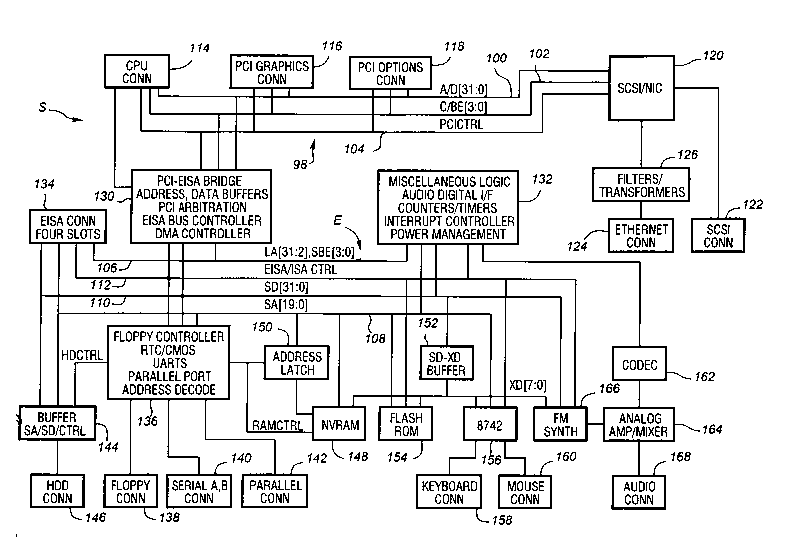
Referring now to Figure 1, the system board S of a
computer system according to the present invention is
shown. In the preferred embodiment, the system boards
contain circuitry and slots for receiving
interchangeable circuit boards. In the preferred
embodiment, there are two primary buses located on the
system board S. The first bus is the PCI or Peripheral
Component Interconnect bus 98 which includes
address/data portion 100, control and byte enable
portion 102 and control signal portion 104. The second
primary bus on the system board S is the EISA bus E.
The EISA bus E includes LA address portion 106, SA
address portion 108, SD data portion 110 and EISA/ISA
control signal portion 112. The PCI and EISA buses P
and E form the backbones of the system board S.
A CPU connector 114 is connected to the PCI bus 98
to receive interchangeable processor cards, such as the
one shown in Figure 2. A PCI graphics connector 116 is
connected to the PCI bus 98 to receive a video graphics
card as shown in Figure 3. A PCI option connector 118
is also connected to the PCI bus 98 to receive any
2 0 ~
-
additional cards designed according to the PCI
standard. In addition, a SCSI and network interface
(NIC) controller 120 is connected to the PCI bus 98.
Preferably the controller 120 is a single integrated
circuit and includes the capabilities necessary to act
as a PCI bus master and slave and the circuitry to act
as a SCSI controller and an Ethernet interface. A SCSI
connector 122 is connected to the controller 120 to
allow connection of various SCSI devices, such as hard
disk drives and CD-ROM drives. An Ethernet connector
124 is provided on the system board S and is connected
to filter and transformer circuitry 126, which in turn
is connected to the controller 120. This forms a
network or Ethernet connection for connecting the
system boards and computer to a local area network
(L~N) .
A PCI-EISA bridge 130 is provided to convert
signals between the PCI bus 98 and the EISA bus E. The
PCI-EISA bridge 130 includes the necessary address and
data buffers and latches, arbitration and bus master
control logic for the PCI bus, EISA arbitration
circuitry, and EISA bus controller as conventionally
used in EISA systems and a DMA controller. Preferably
the PCI-EISA bridge 130 is a single integrated circuit,
but other combinations are possible. A miscellaneous
system logic chip 132 is connected to the EISA bus E.
The miscellaneous system logic chip 132 contains a
digital audio interface, counters and timers as
conventionally present in personal computer systems, an
interrupt controller for both the PCI and EISA buses P
and E and power management logic, as well as other
miscellaneous circuitry. A series of four EISA slots
134 are connected to the EISA bus E to receive ISA and
EISA adapter cards. A combination I/O chip 136 is
- ~ 6a2~3
connected to the EISA bus E. The combination I/O chip
136 preferably includes a floppy disk controller, real
time clock (RTC)/CMOS memory, two UARTs, a parallel
port and various address decode logic. A floppy disk
connector 138 for receiving a cable to a floppy disk
drive is connected to the combination I/O chip 136. A
pair of serial port connectors are also connected to
the combination I/O chip 136, as is a parallel port
connector 142. A buffer 144 is connected to both the
EISA bus E and the combination I/O chip 136 to act as a
buffer between the EISA bus E and a hard disk drive
connector 146 to allow connection of an IDE-type hard
disk drive. A non-volatile random access memory
(NVRAM) 148 is connected to the EISA bus E and receives
its control signals from the combination I/O chip 136.
An address latch 150 is connected to the EISA bus E and
controlled by the combination I/O chip 136 to provide
additional addressing capability for the NVRAM 148.
Preferably the NVRAM 148 is used to contain certain
system information. A data buffer 152 is connected to
the SD portion of the EISA bus E to provide an
additional data bus XD for various additional
components of the computer system. The NVRAM 148 is
connected to the XD data bus to receive its data bits.
A flash ROM 154 receives its control and address
signals from the EISA bus E and is connected to the XD
bus for data transfer. Preferably the flash ROM 154
contains the BIOS information for the computer system
and can be reprogrammed to allow for revisions of the
BIOS. An 8742 or keyboard controller 156 is connected
to the XD bus and EISA address and control portions 108
and 112. The keyboard controller 156 is of
conventional design and is connected in turn to a
keyboard connector 158 and a mouse or pointing device
2l6a2~
connector 160.
The computer system of the preferred embodiment
also includes audio capabilities. To this end a CODEC
chip 162 is connected to the miscellaneous system logic
chip 132 and to an analog amplifier and mixer chip 164.
An FM synthesizer chip 166 is connected to the analog
amplifier and mixer 164 and receives digital
information from the XD bus. The FM synthesizer 166 is
also connected to the control and data portions 110 and
112 of the EISA bus E and is controlled by the
miscellaneous system logic chip 132. An audio
connector 168 is provided to allow external audio
connections to the computer and is connected to the
outputs and inputs of the analog amplifier and mixer
164.
Referring now to Figure 2, the processor board P
is shown. In the processor board P of Figure 2, the
CPU or processor 200 can be any of a plurality of
processors, such as the 486DX/33, 486DX2/66, 486DX4/50-
100, 486DX4/33-100, 486DX4/33-83, P24T, Pentium 50/75,
Pentium 60/90, and Pentium 66/100, and other similar
and compatible processors. The processor 200 provides
data, address and control portions 202, 204 and 206 to
form a processor bus PB. A level 2 (L2) or external
cache memory system 208 is connected to the processor
bus PB to provide additional caching capabilities to
improve performance of the computer system. The L2
cache 208 can be organized as a 128 kbyte direct mapped
cache or 256 kbyte two-way set associative cache when
used with 486 family processor and as a 256 or 512
kbyte direct mapped or two-way set associative cache
when used with Pentium family processors. A cache and
memory controller (CMC) and PCI bridge chip 210, is
connected to the control portion 206 and to the address
Q O
-
portion 204. The CMC 210 is connected to the L2 cache
208 as it incorporates the cache controller and
therefore controls the operations of the cache memory
devices in the L2 cache 208. The CMC 210 is also
connected to control a series of address and data
buffers 212. The data buffers 212 are utilized to
handle memory data to a main memory array 214. The
data buffers 212 are connected to the processor data
portion 202 and receive control signals from the CMC
210. The data buffers 212 provide a memory address bus
216 and a memory data bus 218 to the memory array 214.
A memory control signal bus 220 and memory address bus
216 is provided from the CMC 210. Clock distribution
and generation circuitry 222 is associated with the
processor card P and is connected to the CMC 210. A
processor connector 224, such as a card edge, is
provided to be mateably received by the processor
connector 114. The processor connector 224 is
connected to the CMC 210, the data buffers 212 and the
clock distribution circuitry 222 to provide clocks to
the computer system and to provide a PCI interface to
allow the processor 200 to access the PCI and EISA
buses P and E and to allow PCI and EISA bus masters to
access the main memory array 214.
Referring now to Figure 3, an exemplary video
graphics adapter is shown. A video graphics controller
300 is connected to a PCI graphics connector 316, which
is mateably received in the graphics connector 116. A
ROM 302 is connected to the graphics connector 316 and
receives control signals from the video graphics
controller 300. Video memory 304 is used to store the
graphics data and is connected to the video graphics
controller 300 and a digital/analog converter (DAC)
306. The video graphics controller 300 controls the
2 ~ 0
_
operation of the video memory 304, allowing data to be
written and retrieved as required. A video connector
308 is connected to the DAC 306. A monitor (not shown)
is connected to the video connector 308.
It is noted that the above description of a
computer system is provided for completeness and
numerous variations could be developed as apparent to
those skilled in the art.
Referring now to Figure 4, a block diagram of the
memory controller 210 is shown. There are three main
control blocks in the memory controller 210 and three
primary address transfer queues. The three primary
control blocks are the processor control or PCON block
400, the PCI control or ICON block 402, and the memory
control or MCON block 404. The PCON block 400 provides
the interface to the processor bus PB, particularly the
processor address bus 204 and the processor control bus
206. Additionally, the PCON block 400 is connected to
the L2 data cache 208 and provides the necessary
control signals. The L2 cache controller is contained
in the PCON block 400. In addition, the PCON 400
provides signals to control the data buffers 212. The
ICON block 402 provides data buffer control signals to
the data buffer 212 and in addition interfaces to the
PCI bus 98, particularly, the control and address
portions. The MCON block 404 is the memory device
control portion and is connected to the memory address
bus 216 and the memory control bus 220, and
additionally provides signals to control the data
buffers 212. Each of the particular control blocks
400, 402 and 404 control different portions of the data
buffers 212 as will be illustrated.
The memory controller 210 and data buffer 212 are
effectively organized as a triangle or delta so that
- 21602~
16
data transfer can occur between the processor bus PB
and the PCI bus 98, between the processor bus PB and
the memory bus, and between the PCI bus 98 and the
memory bus. To this end the PCON block 400 is
connected directly to the ICON block 402 to provide
read addresses for read operations by the processor 200
to the PCI bus 98. The write addresses are provided
from the PCON 400 to a P2I queue 406. Preferably, the
P2I queue is four operations deep, so that four write
operations can be posted to the queue and thus be
pending at one time. It is noted that in the case of a
64 bit Pentium microprocessor 200, this would translate
to 8, 32 bit PCI bus 98 operations. The output of the
P2I queue 406 is provided to the ICON block 402 to
provide an address stream. In similar fashion, the
read address information and address bank information
is provided from the PCON block 400 to the MCON block
404 for processor reads from the main memory 214. The
write addresses and bank information are provided from
the PCON block 400 to a P2M queue 408, which is again
also preferably four quadword addresses deep, so that
four write operations from the processor 200 can be
posted to the memory array 214 if a Pentium processor
and eight operations if a 486-based processor. The
output of the P2M queue 408 is provided to the MCON
block 404.
The ICON block 402 is connected to the MCON block
404 to provide read addresses and memory bank
information for read operations from the PCI bus 98 to
the memory 214. In addition, the write address
information and bank information is provided from the
ICON block 402 to an I2M queue 410. Preferably, the
I2M queue 410 is capable of posting eight quadword
addresses to provide relatively deep posting from the
`- 21 6~20~
PCI bus 98 to the memory 214. The output of the I2M
queue 410 is connected to the MCON block 404. An SMAP
or system map block 412 is connected to the control
block 400, 402 and 404 to provide various signals as
necessary.
In addition, a signal referred to as M2IABORT is
provided from the ICON block 402 to the MCON block 404
to allow the MCON block 404 to determine when a Memory
Read Multiple operation has been aborted by the PCI bus
master, as well as for other PCI abort operations. For
this discussion, only the Memory Read Multiple case is
of interest and the other cases will not be discussed.
The MCON block 404 provides a snoop request or SNPREQ
signal, the M2I read address that is the address for
memory to PCI read operations and the I2M write address
to the PCON block 400. This allows the PCON block 400
to perform snoop operations with the L2 cache
controller and to provide the operation to the
processor 200 so that the L1 cache controller inside
the processor 200 can also perform a snoop operation.
Snooping of read addresses as well as write addresses
is necessary because the L2 cache controller, and the
Ll cache controller in the processor 200 in certain
cases, are preferably organized as writeback cache
controllers, and therefore, snoop operations must occur
on reads to maintain memory coherency. The PCON block
400 provides the SNPDONE and SNPHITM or snoop done and
snoop hit to modified signals to the MCON block 404 to
allow the MCON block 404 to proceed with the read or
write operations or retry a read operation if
appropriate.
Referring now to Figure 5, more details of the
data buffers 212 are shown. It can be noted that the
data buffers 212 also contain queues 411, 413 and 414
21fi~20~
`
similar to those in the memory controller 210 so that
addresses are tracked in the memory controller 210
while the data is maintained and transferred through
the data buffers 212. The memory controller 210 is
organized to control the data buffers 212 such that the
particular control blocks 400, 402 and 404 control
their respective portions of the data buffers 212. For
example, the PCON block 400 controls the latching of
data from the processor data bus into the various
registers and the output enable or driving of the data
from the memory onto the processor data bus 202.
Similarly, the ICON block 402 handles latching of data
into the various registers from the PCI bus 98 and the
output enables of the data to the PCI bus 98. The MCON
block 404 handles the operation of shifting data
through the various queues 411, 413 and 414, driving
data from the queues 411, 413, 414 to the actual memory
devices and latching data as required from the memory
devices into either the I2M queue 414 or to registers
as provided to the processor data bus 202 and the PCI
bus 98. It is noted that the processor to memory and
processor to PCI queues 411 and 413 are unidirectional
in the data buffers 212 but the PCI to memory queue 414
is operated bidirectionally, that it is used for both
write data and the read ahead data. Operation will be
clearer according to the description below.
One of the features of the memory controller 210
of the preferred embodiment is that it allows great
flexibility in the use of various speed microprocessors
and various speed DRAM devices in the memory array 214.
Indeed, it allows the memory devices to vary from bank
to bank, the main memory array 214 preferably being
formed of eight banks or modules. The memory
controller 210 of the preferred embodiment allows three
~16~20~
.
19
different memory speeds to be utilized, with each bank
being designated as one of the particular speeds. Each
particular memory speed then has a series of parameters
relating to timing values as commonly utilized in DRAM
specifications. For each particular memory speed, a
value to indicate the row address hold time from RAS*
is provided, the column address set up times to the
CAS* strobe for both reads and writes are provided, the
row address set up time to the RAS* signal is provided,
as is the memory data set up time to the CAS* strobe
and the pulse width of the CAS* strobe. In addition,
the RAS precharge time is provided for each memory
speed. An indication of when the cycle ready signal is
provided to the processor 200 or PCI bus 98 is also
indicated as a timing parameter. Preferably, these
timing parameters utilize 10 bits of memory in a 16 bit
register, the organization shown in Table 1.
~160~
TABLE I
Memory Timing Control Register
Bit 15 Reserved
Bits[14:13] RAS precharge
00 = 2 clocks
01 = 3 clocks
10 = 4 clocks
11 = 5 clocks
Bits[12:11] MRDY read state
00 = Assert MRDY in the C1 state
01 = Assert MRDY in the C2 state
10 = Assert MRDY in the C3 state
11 = reserved
Bits[10:9] reserved
Bit 8 CAS pulsewidth
0 = 2 clocks
1 = 3 clocks
Bits[7:5] Reserved
Bit 4 MD setup to CAS
0 = 1 clock setup time
1 = 2 clocks setup time
Bit 3 Row Address Setup to RAS
0 = 1 clock setup time
1 = 2 clocks setup time
Bit 2 Column Address Setup to CAS, writes
0 = 1 clocks setup time
1 = 2 clocks setup time
Bit 1 Column Address Setup to CAS, reads
0 = 1 clocks setup time
1 = 2 clocks setup time
Bit 0 Row Address Hold from RAS
0 = 1 clock hold time
1 = 2 clocks hold time
216û2~0
_
RAS Precharge defines the number of
clocks in which all RAS* signals must be
negated (high) before any are allowed to be
asserted (low) again.
MRDY read state defines which CAS state
MRDY should be asserted for a memory data
read. If the CAS pulsewidth is two clocks
wide, C2 is skipped. The MRDY state varies
on clock frequency and memory speed.
CAS pulsewidth defines how many clocks
CAS* signals must be held asserted.
MD Setup Time to CAS defines how many
clocks the MD bus must be driven from the
data buffers 212 before CAS* is asserted for
a write.
Column Address Setup to CAS, writes
defines the number of clocks after the Column
Address is generated before CAS* can be
asserted for a write cycle.
Column Address Setup to CAS, reads
defines the number of clocks after the Column
Address is generated before CAS* can be
asserted for a read cycle.
Row Address Hold from RAS defines the
number of clocks after RAS* asserts before
the Row Address may change.
Referring then to Figure 6, each memory bank
includes a related register 500, 502 and 504 to
indicate the ending address of the particular memory
bank. These addresses can be written by the processor
200 after determining the particular size of the memory
module located in the particular bank. The output of
the bank end address registers 500, 502 and 504 are
2 ~ 0
then provided as one input to comparators 506, 508 and
510. A second input to the comparators 506, 508 and
510 is provided by the memory address of the particular
module such as the processor bus PB or PCI bus 98 as
5 appropriate. It is noted that only three of the eight
banks are shown for simplicity. The comparators 506,
508 and 510 have two outputs and a third input. One
output is the less than output, so that if the provided
memory address is less than the ending address of the
particular bank, and there is a carry in value to
indicate enabling of the comparator, the less than
value is true or high, indicating that this is the
selected bank. The comparator second output is a
greater than or equal to signal, which is used to
enable the next comparator. For example, comparator
506 has its greater than or equal to output connected
to an enable input of the comparator 508 such that if
the memory address is greater than or equal to the
address provided in the bank 0 end address register
500, the comparator 508 is activated. If the address
is then less than the bank 1 ending address as stored
in the register 502, then the output of the BANK 1
signal of the comparator 508 iS activated. If the
memory address is instead higher, then this chain
continues to determine if the memory address is less
than that contained in any of the banks. Therefore,
there are eight particular bank outputs, BANK O to BANK
7, to indicate the presence of the memory address in
the particular memory bank.
These BANK 0 to BANK 7 signals are provided to a
memory bank value encoder 512, which provides the BANK
<2: 0~ signals, which are stored along with the write
address values in the I2M queue 410 or P2M queue 408,
for provision to the MCON block 404.
U J
-
As noted above, each bank could be one of three
particular memory speeds, and these indications are
contained in registers 514 and 516. Only two registers
are shown for simplicity. The outputs of the registers
514 and 516 are two bits to indicate the particular
speed, and these bits are provided to the inputs of an
eight input, 2 bit multiplexor 518 whose select input
is connected to the BANK <2:0> signals. The BANK <2:0>
signals are provided with the particular address, be it
read or write addresses for the PCON block 400 or the
ICON block 402, to the multiplexor 518 so that the
output of the multiplexor 518 is the particular two
bits that indicate the bank for the particular address
for which the MCON block 404 is about to execute the a
memory operation. The output of the multiplexor 518 is
connected to the select input of a 3 input multiplexor
520. The multiplexor 520 is connected to the registers
522, 524 and 526 which contain the memory speed timing
values for speed 0, 1 and 2, respectively. These
memory timing values are those indicated in Table 1.
The output of the multiplexor 520 is timing values as
utilized in the state machines and logic described
below for the MCON block 404. In addition, the address
values <27..3> and byte enable or BE* <7..0> signals
are also provided to the MCON block 404 as they have
been tracked through the queues 408 or 410 or are
provided directly on read operations. Therefore, the
memory bank speed timing values are directly provided
by first decoding the particular bank, then having a
look up for the bank based on the previously defined
and stored memory speed value of the optional memory
speed settings, and then selecting the particular
memory speed values for operation for that particular
memory cycle.
21 6~2~-0
An example of the timing values for the preferred
embodiment for three processor speeds and two memory
device speeds is shown in Table II.
TABLE II
Memory Timing Control Combinations
Parameter 33MHz 50MHz 60MHz
6Ons ¦ 7 Ons 6Ons ¦ 7 Ons 6Ons ¦ 7 Ons
RAS precharge 2 2 3 3 3 4
MRDY assertion state C1 C1 C3 C3 C2 C3
CAS pulsewidth 2 2 2 2 2 3
MD Setup 1 l 1 1 2 2
Write Column Addr Setup
Read Column Addr Setup
RA hold 1 1 1 2 2
Memory Timing Control 00_00 00_00 30_00 30_01 20_11 51_10
15 Register (hex value)
The DRAM device speeds can be determined by
~ reading encoded bits conventionally provided on SIMMs
and checking the size. These two parameters are then
used in a lookup table to determine SIMM speed. This
technique is described more fully in Serial No.
08/034,105, filed March 22, 1993, which is hereby
incorporated by reference. With the DRAM device speed
then known for each bank and microprocessor speed known
by other encoded bits, these two parameters are then
used in a second lookup table to obtain the binary
value to be placed in the timing value register for
that continuation. The computer system designer knows
the various propagation delays of the various paths and
can then simply use the clock speed and memory timing
parameters provided by the memory device manufacturer
to determine the timing values for each combination.
_. 216~
ProceeA;ng then to Figure 7, the use of the
addresses, byte enables and timing values are shown as
being provided to a portion of the MCON block 404. The
processor write request, processor read request,
refresher quest, PCI read request and PCI write request
signals are inputs to an arbiter 550 along with signals
referred to as I2CAMHIT, I2MO_EMPTY and P2MO_EMPTY.
The various request signals are an indication that
operations are pending for the memory controller to
operate on from the indicated sources of the indicated
type. Development of these signals is not fully
described but can be readily developed by one skilled
in the art. The outputs of the arbiter 550 are the
P2M, M2P, I2M and M2I signals to indicate which source
and direction of operation has occurred, that is P2M
for a processor to memory write, M2P for a processor to
memory read, I2M for a PCI to memory write operation
and M2I for a PCI read operations. These four signals
are provided as the select signals to a four input
multiplexor 552 which receives the particular read or
write addresses, the byte enables, the memory timing
values and the bank indications for the particular
source. The P2M queue 408 provides write addresses,
byte enables, memory timings and bank information from
the queue 408 for processor to memory write operations,
while the read addresses, byte enables, memory timings
and bank information are provided directly for
processor reads in the M2P case. Similarly, the I2M
queue 410 provides write addresses, byte enables,
memory timings and bank information from the I2M queue
410, while the read addressing information is provided
directly from the ICON block 402 to the MCON block 404.
The output of the multiplexor 552 is the particular
address value, the byte enables, the bank value to
21~020û
indicate which particular bank and the memory timing
values for the particular memory operation to be
performed by the memory controller 210 to access the
necessary memory location for either a read or a write
as appropriate. It is also noted that a page hit
detector 554 is connected to the output of the
multiplexor 552 to provide a PAGEHIT signal to allow
the memory controller 210 to determine whether a page
hit has occurred, so that it can operate the DRAM
devices in the desired page mode operation for best
performance.
Proceeding then to Figure 8, blocks representing
various state machines and other logic utilized in the
MCON block 404 are shown. A number of state machines
provide the actual information and control functions
and are interlocked. The primary state machine is the
MEMSM or memory state machine 600. The memory state
machine 600 receives the memory timing values from the
multiplexor 552 and the M2IABORT signal from the ICON
block 402. A precharge state machine 602 is provided
to provide a signal referred to as RASPCHG or RAS
precharge to indicate that the precharge time for the
particular memory bank is completed if page mode
operation is not occurring. The RASPCHG signal is
provided to the memory state machine 600.
Additionally, RASUP or RAS up logic 604 provides a
RAS_UP signal which is utilized by the memory state
machine 600 to determine whether to leave the RAS* or
row address strobe signal high or low when no memory
cycles are pending, thus providing a prediction whether
the next operation will be a page hit or page miss to
thereby improve performance. Detailed operation of
this logic will be described below.
2160200
A refresh state machine 606 iS provided to control
refresh operations but will not be described in detail
in this description because its operation is relatively
conventional and is omitted for clarity. A memory
5 address state machine 608 receives the timing values
from the multiplexor 552, as well as the basic clock
signal of the system and provides interlock signals to
the memory state machine 600, the MSELRA or memory
select row address signal and the MWE* or memory write
enable signal. The MSELRA signal is provided to the
select input of a 2: 1 multiplexor 610 which receives at
its inputs the memory addresses appropriately connected
to provide row and column addresses based on the
selection input. A burst address block 612 is provided
15 and connected to the column addresses to simplify burst
operation. The outputs of the multiplexor 610 are the
memory addresses provided to the memory array 214 over
the memory address bus 216 for the particular
operation. The MWE* signal is similarly the memory
20 write enable signal as provided to the main memory
array 214. A memory data control state machine 614 is
provided. It receives certain of the memory timing
values and provides interlock signals to the memory
state machine 600 and controls the operation of
25 pertinent portions of the data buffers 212.
The memory state machine 600 provides the MRAS or
master RAS and MCAS or master CAS signals. The MRAS
signal is combined with the bank value signals for the
particular memory operation to provide the RAS*<7:0>
signals which are provided to the particular banks. If
the bank value indicates that this is the particular
bank value for the operation, then the RAS logic 616
directs the MRAS signal to that particular bank in an
inverted form. If the bank value is not the one
_ . 216~2~1~
28
particularly being addressed, then the RAS* signal for
that particular bank is held high to allow the memory
devices to be fully precharged. The MCAS signal is
provided to CAS logic 618 which also receives the BE*
<7:0> signals for the preferred 64 bit width. These
signals provide the eight byte lanes of information
that are encoded with the MCAS signal to produce the
CAS*<7:0> signals which are used to enable the
particular memory devices of the bank indicated by the
lo RAS*<7..0> signals. If a particular byte enable is not
activated, then its related CAS* signal is not
activated, and therefore the memory device is not
selected as it does not receive a column address. This
allows the use of a single MME* signal, with the CAS*
signal providing the byte lane encoding.
The queues 406, 408 and 410 are organized as a
series of registers of the appropriate width.
Particular registers in each queue are selected based
on three particular counter values associated with each
queue. The three counters are the read location
counter, the write location counter and the data
contents counter. The read location counter is
utilized to determine the particular location of the
four or eight registers from which the read data for
the next cycle is to be obtained and provided to the
particular block. The write location counter is
utilized to indicate the particular register into which
data is to be written in the next operation. The read
and write location counters increment on each read and
write operation, respectively, and thus operate in a
circular fashion. The data contents counter is
utilized to indicate whether there is actually data in
the queue. The data contents counter is an up/down
counter. The data contents counter counts up on a
~ 16~200
write operation to the queue and decrements on read
operations. If the data contents counter indicates
that the queue is full by being at a maximum value,
then data is not written into the queue until data has
been removed from the queue. These counters are
conventional logic and are not shown for simplicity and
clarity. I2MQ_EMPTY and P2MQ_EMPTY signals thus
correspond to the data contents counters being at a
zero value.
Because of the length of the I2M queue 410, it is
organized as a content addressable memory or CAM. I2M
queue registers 640 and 642 are shown in Figure 9, with
many omitted for simplicity. The output of the
particular register 640, 642 is not only provided to
the MCON block 404 via a multiplexer but is also
provided to an associated comparator 644 and 646. The
second input of the comparator 644 and 646 receives the
processor address being provided on the processor
address bus 204. The comparators 644 and 646 have
equal outputs so that if the address being provided
directly on the processor address bus 204 is equal to
one of the addresses contained in the I2M queue 410,
then the particular comparator provides its equal
signal true. The equal signal output goes to one input
of an AND gate 648 and 650. The second input to the
AND gate 640 and 650 is provided by a valid bit
register 652 and 654. If data is not contained in the
particular register 640, 642 in the I2M queue 410, then
the valid bit register is set to 0, whereas if data is
present, then the bit is set to 1. These valid bit
registers are set when data is written into the I2M
queue 410 and cleared when data is read out of the
queue 410. In this manner, if the register is valid
and the comparator determines that there is an
21 fiO200
equality, the output of the particular AND gate is set
to a one value to indicate that a hit has occurred.
The outputs of the AND gates 648 to 650 are provided to
an eight input OR gate 654 whose output is the
I2MCAMHIT signal, which is provided to indicate that
the particular read address being requested by the
processor is actually present in the I2M queue 410 as a
write operation from the PCI bus 98, and therefore the
memory read request from the processor 200 cannot occur
until the particular location has been flushed out of
the I2M queue 410. Operation of this delay is seen in
the arbiter 550 as described below.
13 In the preferred embodiment, there are five
14 possible requests for the main memory 214: a processor-
to-memory write (P2M), a memory-to-processor read (P),
a PCI-to-memory write (I2M), a memory-to-PCI read
(M2I), and refresh. A P2M write refers to a write to
the memory 214 and a M2P read refers to a read of the
memory 214, both initiated by the microprocessor 200.
An I2M write refers to a write to the memory 214 and a
M2I read refers to a read of the memory 214, both
initiated by a PCI bus master. All memory requests
from EISA bus masters are passed through the PCI-EISA
bridge 130, which includes the necessary logic to be a
bus master on the PCI bus 98. Thus, any EISA
originated memory request is effectively a memory
request asserted by the PCI-EISA bridge 130.
Generally, the priority of the memory requests are
as follows, with some exceptions: (1) second refresh
request; (2) P2M write request; (3) M2P read request;
(4) I2M write request; (5) M2I read request; and (6)
first refresh request. The second refresh request
indicates that two refreshes are outstanding. When
that occurs, the memory controller 234 gives both
216~2~)0
31
outstanding refresh requests the highest priority,
executing both refresh cycles. The P2M write request
is always higher in priority than other memory requests
except the second refresh. However, if the I2M queue
410 is full or the I2M queue 410 is not empty and a PCI
bus 98 read is outstanding, a signal M_P2M_NOPOST is
asserted to prevent further queuing of P2M write
requests until a PCI write operation is completed.
This allows the P2M queue to clear out, thereby
allowing requests from the PCI bus 98 to be serviced.
However, assertion of the signal M_P2M_NOPOST does not
prevent writeback cycles from being queued, as the
writeback may be needed by the PCI memory request.
The M2P read request is always lower in priority
15 than the P2M write request, but it is usually higher in
priority than I2M write and M2I read requests. The
operation can only occur when the P2M queue 408 is
empty. However, an unlocked M2P read request is forced
lower in priority than an I2M write request if the M2P
20 read is to the same address as an I2M write pending in
the I2M queue. When this occurs, the M2P request
remains lower in priority than I2M requests until the
I2M write request having the matching address is
written to the main memory 214. A M2P read request is
25 also forced lower in priority than an I2M write request
if the I2M queue is full. Additionally, if an M2I read
request is asserted while an I2M write request is
pending, the I2M write request is forced higher in
priority than the M2P read request to allow the I2M
queue to clear, thereby allowing the M2I request to
proceed. Further, an M2I read request is forced higher
in priority than the M2P read request if the M2I read
has been waiting for the M2P request to negate for more
than one arbitration cycle.
2~60203
_
The I2M write request is always lower in priority
than the second refresh request, the P2M write request,
and it is generally lower in priority than the M2P read
request with the exceptions noted above. The I2M write
S operation can only occur when the P2M queue 408 is
empty. The I2M write request is always higher in
priority than the M2I read request. The I2M write
request is held off if the processor is performing a
locked access of the main memory 214. Thus, for a
locked processor cycle, the exceptions discussed above
do not apply to override the higher priority of M2P
read requests over I2M or M2I requests.
A locked or atomic access of the main memory 214
is indicated by a signal LOCK* driven by the
15 microprocessor 200. A locked cycle allows the
microprocessor 200 to read an address location in the
main memory 214 and be assured that the accessed
location is not changed by another bus master before
the microprocessor 200 writes back to the same memory
20 location. These type cycles are referred to as read
modify write cycles. Locked cycles are also generated
during other bus transfers, such as during execution of
the XCHG (exchange) instruction when one of its
operands is memory-based, when updating a segment or
25 page table entry, and when executing interrupt
acknowledge cycles.
The M2I read request is always lower in priority
than the second refresh request, the P2M write request,
and the I2M write request. However, it is higher in
priority than the unlocked M2P read request in the
instance noted above. The M2 I read operation can only
occur when the P2M queue 408 is empty.
Finally, the first refresh request is always lower
in priority than any of the other requests. However,
2 0 0
as noted above, when the second refresh request is
asserted, both the first and second refresh requests
are executed regardless of whether other requests are
pending.
Further details of this arbitration are provided
in Serial No. 08/324,011 , entitled ~System for
Arbitrating Access to Memory~ filed concurrently
herewith, which is hereby incorporated by reference.
Referring now to Figure 10 the memory state
machine 600 is shown in detail. Indications in italics
next to a particular state bubble indicate the value of
various output signals, developed by the state machine.
In this case the MRAS and MCAS signals. The phrases
adjacent to an arrow going from one bubble to an other
are the logical conditions on which that path is taken.
If a path does not have an adjacent logical condition,
that path is taken in all other cases. Transitions are
made on the rising edge of the processor clock signal.
Upon reset of the computer, operation of the state
machine 600 transfers to the RI or RAS idle state. In
this state the MRAS signal is not asserted if the next
state is not state R1. If the next state is Rl, then
the MRAS signal is set to the value 1 or asserted so
that the row address strobe signal is provided. The
MCAS signal is negated to a zero level. Control
proceeds from state RI to state R1 if the M2P condition
is true so that a processor read operation is
occurring, if a PCI read operation is occurring (M2I)
which has not been aborted (!M2IABORT) and is not being
cleared (!CLRI2Mj, or if a write operation from the
processor or the PCI bus is occurring; the row address
ready signal (RADRRDY) is true, which indicates that
the row address set up time to the RAS signal has been
-
- 216Q~
34
met as indicated by the memory address state machine
608, or, if in a processor read case there is no wait
signal indicated as would be appropriate if an aborted
memory to PCI read ahead is completing (WAITRADRRDY)
and the row address set up time two (RADSETUP2) signal
is not activated which indicates that relatively fast
memory is present; a refresh cycle is not occurring
(RFSH_ON); the current read cycle to the PCI bus 98 is
not being aborted (M2IABORTCUR); and the precharge
period has completed for as indicated by the RASPCHG
signal. The M2IABORT signal is provided by the ICON
block 402 as described above. The M2IABORTCUR signal
indicates that the cycle currently being performed by
the MCON block 404 is to be aborted or terminated as
soon as possible. The M2IABORTNEXT signal indicates
that the next M2I cycle which is pending is to be
aborted, which occurs by simlpy skipping the cycle.
The development of the CLRI2M signal is detailed below,
but briefly indicates that a snoop read hit to a
modified location has occurred, so that the I2M queue
414 must be flushed and the read cycle reexecuted.
Therefore, if a memory cycle is indicated, the row
address set up time has been met, and the device is
precharged, control proceeds in state RI to state R1.
In all other cases control remains at state RI.
In state R1 the MRAS signal is set to 1 or high
and true, and the MCAS signal is set low to indicate
that this is a RAS only portion of the cycle. Control
proceeds from state R1 to state R2 if the RADHLD2
signal is true, which indicates that two clock periods
of hold time are required and therefore the
intermediate R2 state is required. If the RADHLD2
signal is not true, then only 1 clock of hold time is
required from the activation of the RAS* signal and
~l60~ao
control proceeds directly from state Rl to state R3.
In state R2, the MRAS signal is asserted and the MCAS
signal is negated. Control proceeds from state R2 to
state R3 on the next rising edge of the processor clock
signal.
In state R3, the MRAS signal is true or high,
while the MCAS signal is set high if the next state is
to be state C1 and otherwise the MCAS signal is set
low. Control proceeds from state R3 to state Cl, the
first of the column states, if the column address ready
(CADRRDY) signal is true as provided by the memory
address state machine 608 to indicate that the
particular column address set up time, be it read or
write, has been satisfied and either a PCI read
operation is occurring or a memory to processor bus
read operation is occurring, and the memory operation
is not stalled waiting for read data; or a write
operation from the processor to memory or the PCI bus
to memory is occurring with the data being valid as
indicated by the MDVALID signal which is provided by
the memory data state machine 614. Therefore, if the
column address set up time has been met and indication
of write operation data being properly valid for write
cases is provided, control proceeds from state R3 to
state Cl. Otherwise, control remains in state R3
waiting for the timing conditions to be satisfied.
In state Cl, both the MRAS and MCAS signals are
high to indicate that the CAS portion of the cycle is
occurring. Control proceeds from state Cl to state C2
if the CASPW3 or CAS pulse width 3 clock signal is
true. If the CASPW3 signal is not true, control
proceeds directly from state Cl to state C3, with
control always proceeding from state C2 to state C3 on
the next rising edge of the processor clock signal. In
- ~1 6û2QO
36
state C2, the MRAS and MCAS signals are both also true.
Thus, state C2 is skipped if the CAS pulse width can be
narrower, as would be true for faster memory or slower
processors with an additional clock period provided
when necessary.
In state C3 the MCAS signal is negated to a 0
level to indicate completion of the particular memory
cycle and the MRAS signal is set to 0 if the next state
is the RI state or if the particular cycle is aborting.
Otherwise, the MRAS signal remains in a high or
asserted state to allow operation in page mode if
appropriate. Control proceeds from state C3 to state
RI if a burst operation is not occurring, which is a
preferable operation for 486 and Pentiun processors, or
the current memory to PCI read cycle is being aborted
as explained below; the next memory to PCI read
operation is not aborted; there is no indication that
the M2I cycle is to be aborted as indicated by the
M2IABORT signal or the CLRI2M signal; and a non-refresh
cycle is occurring (M2P+ADDRRDY) and this is not a page
hit; a refresh cycle is occurring or there is no cycle
pending and the RAS_UP signal is true, indicating that
the RASUP block 604 has indicated that the prediction
is for the next cycle to be a page miss. The RAS_UP
signal is generated as follows:
RAS_UP = !((!WRITEBACK && P2M) ll (!MDATARD && M2P) ll
(!Q_I2MQEMPTY && I2M) II (!M2IABORTCUR &&
M2IMULREAD && !M2IABOKl~xl) ll HIT2MOD)
Therefore, the RAS* signal is kept low or in page mode
following processor to memory write operations which
were not writebacks from the Ll or L2 caches, processor
code read operations, PCI bus write operations with
2~6Q20~
-
pending write operations, Memory Read Multiple
operations from the PCI bus 98 which are not being
aborted, or hits to a modified address, indicating that
a writeback operation has just occurred. In all other
S cases the RAS_UP signal is true, such that it is
considered better to initiate a full new page access to
allow precharging to occur during the idle period.
If the conditions for transfer from state C3 to RI
are not true, control proceeds from state C3 to state
RN or the RAS low idle state. In this state the MRAS
signal is low if the next state is state RI otherwise
the MRAS signal is asserted. The MCAS signal is
asserted if the next state is Cl, otherwise the MCAS
signal remains in low state. Control proceeds from the
RN to C1 state for burst operations in general if the
column address set up time has been met and there are
no abort operations occurring. Control proceeds from
the RN state to the RI state under conditions which
generally indicate that the cycle is being aborted or a
processor non-burst read which is a page miss is next
to occur. In all other cases, control remains at state
RN, idling with the RAS* signal low until a cycle needs
to be run or an abort or page miss occurs. Therefore,
it can be seen that the memory state machine 600 drives
the MRAS and MCAS signals based on the timing values of
the proper bank, these timing values being variable as
indicated above.
A memory address state machine 608 is shown in
Figure 11. The state machine 608 starts at state RAI
upon reset. In this state, the RADRRDY signal and
CADRRDY signals are set low to indicate that the row
and column addresses are not ready, and the MSELRA
signal is set high to initially select the row address
to be provided to the memory devices. The MWE* signal
21602~0
-
38
is set to 1 or negated level on reset and after entry
into the RAI state and is set equal to the CHl state
value the first state after entry from the CHl state as
described below. Control proceeds from the RAI state
to the RHl state if an active cycle is pending from the
PCI bus 98 or processor 200 and the next cycle in the
read ahead operation is not to be aborted. The current
M2I read cycle is aborted under certain conditions,
such as receipt of M2IABORT signal or a writeback is
occurring, while the next M2I read cycle is aborted
when the M2INA signal has been received but the cycle
not started when the M2IABORT signal is received. In
all other cases control loops at state RAI.
In state RHl the CADRRDY signal is set low and the
RADRRDY signal is set to the value of M2P or memory to
processor read upon entry from the RAI state, is equal
to 0 on entry from the CH2 state as defined below and
after entry into the RHl state is set to a 1 level.
The MSELRA and MWE* signals are set to high levels so
that the row address is selected and a write operation
is not indicated. Control proceeds from the RHl to the
RH2 state if the MRAS signal is true from the memory
state machine 600 and the RADHLD2 signal or row address
hold time signal is set to indicate slower memory
devices. If the MRAS signal is true and the RADHLD2
signal is not set, control proceeds from the RHl state
directly to state CHl, which is also where control
proceeds on the next clock signal in the RH2 state. In
all other cases, operation loops at the RHl state. In
the RH2 state, the RADRRDY signals and CADRRDY signal
are set low, and the MSELRA and MWE* signals are set at
high state. Control proceeds from the RH2 to the CHl
state.
2l6a20~
In the CH1 state, the RADRRDY signal is low to
indicate that the row address set up time has not been
met. The CADRRDY signal is set to a high or true value
after initial entry into the state. On entry the
CADRRDY signal is set high if short CAS address setup
times were set (!CADSETUP2) for the read or write as
appropriate, and otherwise is set low. The MSELRA
signal is set to 0 to indicate that the column
addresses are selected and the MWE* signal is low if a
write operation is occurring.
Control proceeds from the CHl state to the RAI
state if the memory state machine 600 is in state RN
and either the cycle is aborting or a processor read
page miss is pending. Control proceeds from the state
CHl to state CH2 if the memory state machine is not in
state RN or the cycle is not aborting completely or the
processor read cycle is a page hit. In the CH2 state
the RADRRDY and CADRRDY signals are set low to indicate
that no addresses are ready. The MSELRA signal is set
low and the MWE* is set low to indicate the write
operation is occurring and the column addresses are
provided. Control proceeds from the CH2 state to the
CH1 state for ongoing burst cycles when the memory
state machine is in state C3 or for pending processor
read page hit operation. Control proceeds from the CH2
state to the RAI state if the cycle is aborting or if
an idle condition is present and the RAS* signal is to
be set high. Control proceeds from the CH2 to the RH1
state if a processor read page miss operation is to
occur and the memory state machine 600 is at the end of
a cycle.
Therefore the memory address state machine 600
properly provides the MWE* signal for the DRAM devices
and controls the address multiplexor 610. In addition,
-` 216~2~0
the RADRRDY and CADRRDY or row and column address ready
signals are provided to the memory state machine 600
based upon the column and row address set up times as
provided in the memory timing registers.
The MD or memory data state machine 614 is
illustrated in Figure 12. The state machine 614 starts
at the IDLE state upon reset. Control proceeds from
the IDLE state to a RD state for processor or PCI bus
98 read operations which are not being aborted and
refresh is not occurring. Control proceeds to the DCD
state if a processor to memory write operation is
occurring and there is no refresh or if a PCI bus to
memory write operation is occurring and again there is
no refresh. Control otherwise remains at the IDLE
state. Control proceeds from the RD state to the DCD
state if the memory state machine is in states C3 or
RN, the cycle is either being aborted or is not a burst
cycle and it is a write operation with a 33 MHz
processor. Control proceeds from the RD state to the
IDLE state if MRAS is negated and the cycle is aborting
or the memory state machine is in states C3 or RN, the
cycle was not a burst or is aborting, and a non-33 MHz
processor write operation or PCI bus 98 write cycle is
pending or no cycles are active. In all other cases,
control remains at state RD.
Control proceeds from the DCD state to the DH1
state if the MDSETUP2 signal is not true, indicating
that this is a fast memory data set up case, and the
memory state machine 600 is not in state C2 and 33 Mhz
operation is indicated for the processor. In all other
cases, control proceeds from the DCD state to the DS2
state. Control proceeds from the DS2 state to a DS3
state if the processor 200 is not operating at 33 Mhz
and the MDSETUP2 signal is set to indicate slower
~ 6~0
41
memory data set up times. Control proceeds from the
DS2 to DHl states in all other cases. Control proceeds
from the DS3 state to the DS1 state on the next rising
edge of the clock signal.
In the DH1 state, the MDVALID signal is set to 1
or asserted to indicate that the memory data set up
time to the column address strobe has been met. This
allows the memory controller state machine 600 to
proceed to state C1. Control proceeds from the DH1
state to the DCD state if further write operations are
pending and otherwise proceeds to the DH2 state. In
the DH2 state, the MDVALID signal is set to o to
indicate that the memory is no longer valid. The value
of the MDVALID signal is not changed in any states
other than the DH1 and DH2 states, except it is cleared
on reset. Control proceeds from the DH2 state to the
IDLE state if no write operations are pending from the
PCI bus 98 or from the processor 200. In all other
cases, control proceeds from the DH2 state to the DCD
state. In this manner, the memory data state machine
614 provides the MDVALID signal to the memory state
machine 600 when the memory data is properly set up.
The precharge state machine 602 is shown in Figure
13. Upon reset, the state machine 602 operation
commences at state A. Control remains in state A when
the MRAS signal is not asserted. When the MRAS signal
is asserted, control proceeds to one of states B, C, D,
or E, dependent upon the number of clocks defined for
the precharge time. Control proceeds to state B for
five clocks, to state C for four clocks, to state D for
three clocks and to state E for two clocks. Control
proceeds from states B to C to D to E, sequentially,
when the MRAS signal is not asserted. Otherwise,
control remains in each particular state. Control then
21~2~
42
proceeds from state E back to state A when the MRAS
signal is deasserted. Therefore the precharge state
machine 602 leaves state A upon the commencement of a
particular memory operation and then does not begin
traversing the remaining states until the MRAS signal
has been negated, so that a precharge period has
started. It is noted that this results in the proper
precharge time for any given bank, even if banks are
being switched in sequential memory operations if
refresh operations are ignored. This occurs because,
as noted above, when a particular bank is not selected
the RAS* signal for that bank is set high so that it is
in a precharge period. Thus if the bank is not
selected, it has been through at least one full memory
cycle of precharge, which is sufficient to provide the
required recharge in all cases. Thus, the precharge
time is set for that of the particular memory bank on
which the current cycle is operating, so that if back
to back cycles occur on that particular memory bank,
the memory devices are properly precharged.
However, refresh operations somewhat degrade this
operation as it is not known in the preferred
embodiment which bank will be requested after a refresh
cycle, so to simplify the design of the preferred
embodiment, the precharge value for all of the DRAM
types is set to the worst case by the initialization or
POST software. This reduces performance in certain
cases but simplifies the design. A slightly more
complicated design would use the worst case value,
preferably provided to a predetermined register for
only the first precharge operation after a refresh
cycle and thereafter operation would revert to the
optimal timing for each bank.
~lfi~2~0
43
Write addresses and data traverse through the I2M
queues 410 and 414 based on having posted data and the
arbiter 550 providing access to the queues 410 and 414
by the memory system. The write addresses are provided
to the PCON block 400 when placed in the I2M queue 410,
to allow the PCON block 400 to control snooping of the
address by the L1 and L2 cache controllers. Read
operations occur in a different fashion than write
operations. Read addresses are provided to the MCON
block 404 along with an indication that a read request
has issued. The read addresses are provided based on a
return of an L2 cache line, which is 4 32 bit words for
486 microprocessors and 8 32 bit words for Pentium
processors. Therefore, when an M2I read is requested,
four or eight 32 bit words are provided, with the ICON
block 402 properly providing the data from the read
operation to the PCI bus 98 as required. The read
request indications are provided by a memory to PCI
next address state machine described below. The read
request is also provided to the arbiter 550 for
arbitration and to the PCON block 400 to allow L1 and
L2 cache snooping with a writeback in case of a hit to
a modified line. When the arbiter 550 provides the
approval to proceed with the PCI bus 98 read, the MCON
block 404 then proceeds to process the information. It
is noted that this will have occurred only after the
I2M queues 410 and 414 are emptied of any pending write
operations so that the I2M data queue 414 provided in
the data buffer 212 can be utilized to do a block read
operation of the lengths indicated. Therefore, when
the I2M queues 410 and 414 are emptied, the read
operation commences and is controlled by an M2I state
machine as shown in Figure 14. The state machine
commences at state A upon reset. Control then proceeds
216~20~
to state B if the I2M queue 414 is empty, a read is
requested and the L2 cache 208 is not being flushed.
This would be a normal read condition. If instead, the
L2 cache 208 is being flushed, control then proceeds
from state A to state F, assuming that the I2M queue
414 is empty and the read request is present.
Otherwise control remains at state A waiting for the
read operation to be initialized.
From state B, control proceeds to one of four
different states. Control returns to state A if the
M2IABORT signal has been received, indicating that the
PCI bus master has aborted the read operation, or if
the IREQACK signal is true, which indicates that the
next operation as determined by the arbiter 550 will be
a PCI read, and the SNPDONE signal is true indicating
that the PCON block 400 has completed snooping the read
operation address to the level 2 cache and to the level
1 cache in the processor 200. Control proceeds from
state B to state C if the M2IABORT signal is not
asserted, the next cycle is a PCI read as indicated by
the IREQACK signal being asserted, there has not been a
snoop hit to a modified (SNPHITM) location as indicated
by the PCON block 400 and the snoop operation has not
been completed, as also indicated by the PCON block
400. This will be the case where a read operation has
been requested and has been arbitrated but may have to
be aborted because the snoop operation has not been
performed and a hit to a modified location may yet
occur. Control proceeds from state B to state D, if
the operation is not being aborted and a PCI read has
not been arbitrated, but there has been a snoop hit to
a modified location with the writeback operation not
yet completed. Control proceeds from state B to state
E if the cycle is not aborted, has been arbitrated as
- 21~2~
indicated by the IREQACK signal and there has also been
a snoop hit to a modified location, so that a writeback
operation from the appropriate cache controller will be
occurring. In all other cases control remains at state
B.
Control proceeds from state C back to state A if
the cycle is being aborted or if the snoop is completed
without being a hit to a modified location. Control
proceeds from state C to state E if the cycle is not
aborted and there has been a snoop hit to a modified
location. Otherwise, control remains at state C until
the snoop operation is completed, the cycle is aborted
or there is a snoop hit to modified. Control proceeds
from state D back to state A if the operation is
aborted or upon indication that the PCI cycle is next
for operation and the snoop has completed. This would
occur after the writeback has been completed and then
the PCI operation is next to occur, as the write back
will have superseded the PCI operation. Control
proceeds from state D to state E if it is not being
aborted, the PCI request is next and the snoop has not
been fully completed. Otherwise control remains at
state D.
In state E, the CLRI2M signal is set to indicate
to other portions of the memory controller 210 that
because of the writeback, the data in the I2M queue 414
must be flushed and discarded. A CLRI2MDONE signal
indicates this flushing has been completed. Control
proceeds from state E to state F if the cycle is not
being aborted and the signal CLRI2MDONE or clear the
queue done signal is true and the snoop is not yet
completed. Control proceeds from state E to state G if
the cycle is not being aborted, the clearing of the
queue 414 has been completed and snoop has been
C~l 602~;~
-
46
performed. Control proceeds from state E to state A if
the cycle is being aborted and in all other cases
remains at state E.
Control proceeds from state F to state G if it is
not being aborted and the snoop cycle has been
completed. Other control proceeds from state F back to
state A if the cycle is being aborted. Otherwise
control remains at state F. Control proceeds from
state G back to state A if the cycle is aborted or if
it is next in line as indicated by the IREQACK signal.
Therefore, the M2I state machine controls transfer
of information from the memory to the PCI interface
using the I2M queue 414 located in the buffer 212.
Data is not transferred until the queue 414 is cleared
of any write data and then proceeds only based on snoop
information and when the arbiter 550 allows it to
proceed.
As noted above, the design of the preferred
embodiment performs read ahead operations when a PCI
Memory Read Multiple operation has been received. The
operation proceeds as follows. The ICON block 402
receives a Memory Read Multiple cycle form the PCI bus
98 and when there is room in the I2M queue 414 issues
an M2I read cycle request, along with an address, to
the MCON block 404. The MCON block 404 arbitrates as
described above and ultimately starts on the M2I read
request. When it has started the operation, it
provides a next address or M2INA signal to the ICON
block 402 and provides the data to the I2M queue 414
along with the appropriate ready signals. The ICON
block 402 knows a Memory Read Multiple command is
occurring and issues another M2I read cycle request at
the next address when the N2INA signal is received and
the I2M queue 414 can receive another cache line of
21~2~
-
47
data. The ICON block 402 also receives the ready
signals from the MCON block 404 and provides the data
to the PCI bus 98. The MCON block 404 receives the M2I
read cycle request and executes it when the cycle wins
the arbitration. Conventionally this will be before
the ICON block 402 has removed all of the data from the
I2M queue 414 for the initial read request. The MCON
block 404 then commences the read request and issues
another M2INA signal. The MCON block 404 then provides
the data to the I2M queue 414. The ICON block 402
receives this M2INA signal and again checks to see if
there is space available in the I2M queue 414 to
receive another cache line. When there is room because
the ICON block 402 has provided sufficient data to the
PCI bus 98, the next M2I read request is provided to
the MCON block 404. This process continues until
either the Memory Read Multiple completes, a page
boundary is crossed or the PCI bus master aborts the
cycle.
~ 20 The abort case is the one of interest as the
pending read ahead operation is terminated as soon as
possible to save retrieving the entire cache line.
This can be seen in the discussions of the MEMSM 600,
the MADRSM 608, the MDCDSM 614 and the M2I state
machine. This quick termination is seen in the MEMSM
600 as the return to the RI or Cl states from the C3
and RN states, so that the cycles finishes as soon as
the current individual read operation is completed,
thus potentially before the completion of the full
cache line read. Similarly the MADRSM 608 returns to
the RAl state if a cycle has not started or when the
column addresses have been provided. The MDCDSM 614
returns to the IDLE state if no operation has been
started or if the MEMSM 600 is in the C3 or RN states.
~1602û~
48
The M2I state machine returns to the A state whenever
the M2IABORT signal is received. On detection of the
abort, the ICON block 402 determines the end of the
read cycle and resets its pointers to the data in the
I2M queue 414 to indicate that no data is present, thus
effectively ~icc~rding the data which has been read
ahead. Thus the read ahead operation terminates as
soon as possible after the abort indication is
received, saving time by not completing the full cache
line retrieval.
The next address indication to allow the read
ahead is provided by the M2INA or memory to the PCI
next address state machine shown in Figure 15. The
initial read address will have been provided using the
conventional read request mechanism. An M2INA signal
is provided to the MCON block 404 to indicate that the
next read cycle can being. This state machine begins
operation in state A upon reset and proceeds to state B
if the PCI read operation is next as indicated by the
IREQACK signal and is not being aborted. Otherwise,
control remains at state A. Control proceeds from
state B back to state A if the cycle is being aborted
or if the I2M queue 414 is to be cleared because of a
writeback or if the snoop has been completed and the
M2IACK signal is provided indicating that the prior
read operation has been acknowledged by the MCON block
404. Otherwise control remains at state 8. Control
proceeds from state B to state C if the cycle is not
being aborted, it is not necessary to clear the queue,
the snoop operation has not completed and yet an M2IACK
signal has been received. Control proceeds from state
C back to state A if the cycle is aborted, the I2M
queue 414 is being cleared, or the snoop is completed
and otherwise remains in state C. Thus the M2INA state
21~2~0
49
machine returns to idle upon recipt of an abort
indication.
The M2INA signal is provided to the MCON block 404
to indicate that the next address is being provided,
that is, another read request can be issued to keep the
I2M queue 414 filled ahead of the PCI bus 98. The
M2INA signal is provided if the cycle is not being
aborted, the I2M queue 414 is not being cleared, the
snoop of the previous read cycle has completed and the
M2INA state machine is either in state C or in state B
and the M2IACK signal has been received. This M2INA
signal is an indication that the processing of the
prior address is complete by the MCON block 404 and the
processing of the next read address can begin. The
actual incrementing of the read address value is
performed in the ICON block 402 using an 8 bit counter,
thus limiting the total read ahead length to 256
address values. When the counter reaches 255, the read
ahead operation is terminated by logic not illustrated
for simplicity by causing the Memory Read Multiple to
be disconnected. A new address must be received from
the PCI bus master to continue the Memory Read Multiple
Operation.
Therefore a memory controller according to the
preferred embodiment includes many improvements. It is
very flexible, allowing simple yet high performance use
with a plurality of processor and memory device speeds,
allowing flexibility and economics of scale. it
provides improved performance by basing idle state RAS*
signal level predictions on both processor and PCI bus
conditions. It allows very deep write points from
several buses and easily handles the various coherency
issues. It also provides a quick method for ending
2l6a~0
-
read ahead cycles when the basic read operation has
been aborted.
The foregoing disclosure and description of the
invention are illustrative and explanatory thereof, and
various changes in the size, shape, materials,
components, circuit elements, wiring connections and
contacts, as well as in the details of the illustrated
circuitry and construction and method of operation may
be made without departing from the spirit of the
invention.