Note : Les descriptions sont présentées dans la langue officielle dans laquelle elles ont été soumises.
~ WO 95/24743 PCT/US95/01163
21602.~
TRANSMISSION LINE AND METHOD OF DESIGNING SAME
Field of the Invention
Generally, the present invention relates to tr~ncmic.sion lines, and,
more specifically, to balanced trancmic.cion lines having a small cross-
section and methods of designing same.
Background of the Invention
Generally, balanced tr~n.cmi.ccion lines are used to differentially
transmit radio frequency (RF) signals between two circuits. A tranverse
electric and magnetic (TEM) tr~ncmic.cion line traditionally contains at least
15 two conductors for tr~ncmitting the RF signal. The geometries of the two
conductors and the use of a dielectric material cleterminPs the characteristic
impedance and quality of the tr~ncmiccion line. In the past, geometries
such as a broadside-coupled tr~ncmiccion line, illustrated in FIG. 1, a
coplanar tr~ncmi.c.cion line, illustrated in FIG. 2, and a micro strip
2 0 tr~ncmi ccion line, illustrated in FIG. 3, have been used for particular
applications as tr~ncmic.cion lines. However, when attempting to use these
particular geometries in a tr~ncmiccion line having a limited cross-section,
these traditional geometries, illustrated in FIGS. 1-3, failed to provide a
tr~ncmic.cion line having a char~cterictic impedance within a desired range.
2 5 The cross-section refers to the height and width of the tr;~n.cmi.ccion line geometry. These three geometries fail to have a tolerant characteristic
impedance due to manufacturing variations of conductor pattern etch,
conductor pattern registration, and dielectric l:~min~te thickness.
Additionally, the micro strip tr~ncmiccion line is an unbalanced
3 0 tr~ncmiccion line. Thus, it would be advantageous to provide a
wo gs/24743 ~6~ - 2 - PCT/US95/01163
tr~ncmi.c.cion line having limited cross-section with a characteristic
impe-l~3nce within a desired range, and is easily manufacturable.
Brief Description of the Drawings
FIG. 1 is an illustration of a broad-side tr~ncmiccion line geometry that
is prior art.
FIG. 2 is an illustration of a coplanar tr2ncmiccion line geometry that is
prior art.
FIG. 3 is an illustration of a micro strip transmission line geometry that
is prior art.
FIG. 4 is an illustration of the symmetry planes used in accordance
with the present invention.
FIG. 5 is an illustration of a tr~ncmi.ccion line in accordance with the
present invention.
FIG. 6 is a perspective view illustration of the tr~ncmi.ccion line of
FIG. 5 in accordance with the present invention.
FIG. 7 is an illustration of a table cont~ining tolerances measured of a
tr~ncmi.ccion line geometry in accordance with the present invention.
FIG. 8 is an illustration of two tables cont~ining tolerances measured
from a prior art tr~n.cmi.ccion line geometry.
- WO 95124743 PCT/US95/01163
_ 3 21602~7
Description of a Preferred Embodiment
A preferred embodiment of the present invention encompasses a
tr:~ncmiccion line geometry having an improved characteristic impedance
tolerance for a tr~ncmiccion line having a limited cross-section. The
tr~ncmi.ccion line geometry utilizes a unique combination of broadside
coupling and coplanar coupling with a reflector plate in order to improve the
tolerance of the characteristic impedance. First, a larger coplanar gap is
used to reduce the etching error. Second, the inner dielectric thickness
sensitivities were also reduced by relying on broadside coupling and
coplanar coupling to determine the characteristic impedance of the
tr~n.smiccion line. Third, the effect of registration error in the broadside
coupling is elimin~t~d by rendering the two signal bearing conductors on
the same layer.
A broadside coupled tr~ncmicsion line geometry, such as that
illustrated in FIG. 1, has a characteristic impedance that is sensitive to the
thickness of the dielectric material between the first conductor 101 and the
second conductor 103, the registration offset between the first conductor
101 and the second conductor 103, and the width of the first conductor 101
and the second conductor 103. Table 801 of FIG. 8 illustrates the
broadside tr~ncmic.cion line geometry tolerance to inaccuracies in etching or
line ~idth and the dielectric for a 50 ohm tr~ncmiccion line, having a
desired conductor width of 0.39 millimtoters, and a dielectric thickness of
2 5 0.125 millim~ters. As can be seen from table 801, the broadside
tr~ncmiccion line geometry varies by approximately -24.5% to + 27% due
to the variances. Table 803 of FIG. 8 illustrates a relationship of the
tolerance of the broadside tr~ncmiccion line geometry to fluctuations in the
width of the conductors and the offset registration between the first
3 0 conductor 101 and the second conductor 103. As can be seen from the
W O 95/24743 ~6~ PCTtUS95tO1163 --
- 4 -
table 803, broadside tr~ncmiccion line geometry varies between -8% to +
17% for the given registration offset.
The coplanar tr~ncmiccion line geometry as illustrated in FIG. 2 fails to
provide a tr:~ncmiccion line of 50 ohms when the design criteria requires an
5 overall width of the tr~n.cmic.cion line less than 1.6 millim~,ters. The reason
it fails is that a 50 ohm tr~ncmicsion line having conductor width of 1.6
millim.o.ters requires a coplanar gap of 0.025 millim~ters. A gap of this
width is difficult to manufacture with currently available technology for our
given application. The coplanar gap is illustrated in FIG. 2 as the distance
between the first conductor 201 and the second conductor 203, and
designated as Y in FIG. 2.
In order to overcome the shortfalls of the existing trancmiccion line
geometries, a new tr~n.cmiccion line geometry was invented which utilized
characteristics from both the broadside tr~n.cmi.c.cion line geometry and the
l S coplanar tr~ncmic.cion line geometry. Part 1 of FIG. 4 is an illustration of
the symmetry plane from the coplanar tr~n.cmiccion line geometry that is
adopted by the new tr~n.cmiccion line geometry. Part 2 of FIG. 4 is an
illustrate of the symmetry plane from the broadside tr~ncmiccion line
geometry that is adopted by the new tr~n.cmiCcion line geometry.
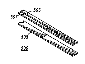
FIG. 5 is an illustration of a trAncmiccion line geometry 500 in
accordance with the present invention. The tr:~ncmicc,ion line geometry 500
includes a first conductor 501, a second conductor 503, and a third
conductor S05. The first conductor 501 and the second conductor 503 are
edge coupled as in a traditional coplanar geometry as shown by capacitors
2 5 507 in FIG. 5. Additionally, the first conductor 501 and the second
conductor 503 are broadside coupled using the third conductor 505 as a
reflector plate, as illustrated by the capacitors 509 shown in FIG. 5. The
effective broadside height is equal to twice the ~lict~nr.e between the third
conductor 505 and a plane formed of the first conductor 501 and the second
3 0 conductor 503. In the preferred embodiment, the first conductor 501 and
the second conductor 503 are used to carry radio frequency signals between
wossn47~3 216O2S7PCTIUS951~1163
a radio receiver and an antenna. The third conductor 505 is a floating
conductor used to contain the electric fields between the first conductor 501
and the second conductor 503; thereby reflecting an image of the conductors
501, 503. Often, the third conductor is referred to as a reflector plate.
5 Typically, the space between the third conductor 505 and the plane of the
first conductor 501 and the second conductor 502 is filled with a dielectric
m~teri:~l Alternatively, the space may be left empty. In the plcrellcd
embodiment, the dielectric m~teri~l iS a flexible circuit board m~teri~l,
commonly referred to as flex, having a dielectric constant, r, equal to 3.4.
1 0 Additionally, the third conductor 505 contains periodic discontinuitiesalong its length to suppress any undesirable tr~ncmiscion modes, such as
transverse electric (TE), transverse magnetic (TM), or transverse electric
magnetic (TEM). The periodic discontinuities are realized by breaking the
third conductor along its length. The electrical distance between the
1 5 periodic discontinuities should be less than one-quarter of the wavelength of
the highest frequency to be tr:lncmitted on the tr~ncmic.cion line 500. In the
pl~fellcd embodiment, the periodic discontinuities occur every one-tenth
wavelength of the highest frequency transmitted on the trzlncmicsion line.
The highest frequency tr:3ncmitted is 1.5 Gigahertz (GHz).
FIG. 7 is a table illustrating the results of the new tr~ncmicsion line
geometry for various tolerances for a 50 ohm tr~ncmiscion line. For the
given tolerances, the characteristic impedance varies -15.2 and +17.2% as
col~ cd to the broadside tolerance which varies between -24.5% to +
27%%. Thus, the new tr~n.cmicsion line geometry allows for a more error
2 5 tolerant tr~ncmic,cion line design for small cross-sections.
In order to design a tr~ncmicsion line using this geometry, the
following process should be followed. First, one determines a desired
physical cross-section of the tr~ncmicsion line including both the height and
the width of the trancmi.c.cion line. In the preferred embodiment, the overall
3 0 height could not exceed 0.311 millim~ters, the inner dielectric was limited to
0.100 millim~ters, and the width of the tr~ncmiccion line could not exceed
W O 95/24743 1 PCT~US95/01163
~6~S
- 6 -
1.6 millimPters Second, one determines a desired tr~n~mission line
characteristic impetl~nce, Zod- In the preferred embodiment, the desired
characteristic impedance, Zod. is equal to 50 ohms. Third, one determines
the highest frequency of tr~nsmi~sion to be used on the tr~n~mi~ion line,
and its corresponding wavelength in the tr~n.cmis~ion line. In the preferred
embodiment, the highest desired frequency of tr~n~mi~sion is 1.5 GHz,
which has a corresponding wavelength in the tr~nsmi~ion line equal to 110
mm. Fourth, one chooses a coplanar gap Y between the first conductor 501
and the second conductor 503. The coplanar gap should be chosen to be as
small as is convenient given the current manufacturing technologies. The
coplanar gap should generate a coplanar characteristic impedance Zoc which
is greater than the desired characteristic impedance Zod- In the preferred
embodiment, the coplanar gap Y was chosen to be equal to 0.25 mm.
Using the coplanar gap Y and the overall width of the tr~n~mission line, one
calculates the maximum equal widths of the first conductor 501 and the
second conductor 503. In the preferred embodiment, the width of the first
conductor 501 and the second conductor 503 are equal to 0.55 mm. Fifth,
one calculates a broadside height between the first conductor 501 and the
second conductor 503 such that the following equation is satisfied.
l/zod = 1lzoc+llzob
This equation is a rough estimate of the effective impedance of the resulting
tr~nsmi~.sion line. In the preferred embodiment, the broadside height is
equal to 0.200 mm. Sixth, one sets the distance between the third
conductor 505 and the plane of the first conductor 501 and the second
2 5 conductor 503 equal to one-half the calculated broadside height. Seventh,
one builds the calculated geometry, then finely adjusts the limPnsionS to get
the desired characteristic impedance. Most likely, the estimate, as a result
of solving the above equation, will give you a lower characteristic
impedance than the desired characteristic impe-l~nre, Zod Before
3 0 m~nllf~ctllring the calcul~ted geometry, accurate modeling can be done by
using a high frequency structure .sim~ tor, such as the High Frequency
WO 95/24743 'i; S,~ PCT/US95/01163
Structure Simulator 85180A available from Hewlett Packard. As an
optional step, one may design periodic discontinuities along the length of
the third conductor 505. These periodic discontinuities or breaks in the
third conductor 505 should be spaced less than one-quarter of the
5 wavelength of the highest frequency to be transmitted along the
tr~ncmiccion line 500. In the preferred embodiment, the periodic
discontinuities were spaced one-tenth of a wavelength of the highest
frequency to be transmitted on the tr~ncmiccion line 500 (20 mm). As the
breaks can be clearly seen FIG. 6 which is a perspective view of the
10 tr~ncmiccion line of FIG. 5.
What is claimed is: