Note : Les descriptions sont présentées dans la langue officielle dans laquelle elles ont été soumises.
21 62302
., ~..
METHOr) AND ~4PPARATUS FOR SEQU~NCING POWER
DELIVERY IN MIXED SUPPLY COMPUTER SYSTEMS
SPECI FICATI~N
CROSS-REFERENCE ~0 RELATED APPLICATION
The present applic~tion is a contin~ation-in-part of IJnited St~tes application Serial
N~ 0~/335,209 (Attorney Docket N 38099) flled November 7, 1994.
The present application m~y be utilized as the re~ulating means for regulating the
5 volt~ge of a power cell and for providing the appropriate voltage ~o a utilization device as
described in U.S application Serial No. 08/384,570 filed on February 6, 19g5. Said U.S.
applioation Se~ial No. 081384,~70 is incorporated herein by reference.
The present invention may also be utilized in conjun~tion with the power source
control circuit for power control during battery ch~ging or as a subcircuit of the power
1 P supply system for supplying the multiple logic voltage levels of a hand held por~able data
terminal as described in U.S. application Sefial No. 08l379,684 filed January 25, 1~55.
Said U.S. application Serial No. 08/379,684 is incorporated herein by reference. TECHNICA~ FIELD
The invention relates generally to power supplies of ccrnputer hardware devices,15 and specifically to systems ~ivhich implemen~ mixed logic volta3e supply levels.
- 2 1 623Q2
BACKGROIJND ART
Computer systems are beçomin~ ,easingly rnore portable while at the sarne time
becoming increasingly mo~e powerful. Low power consumption is an essential design
5 criterion of portable l~attery powered computer systerns and data terminals. For this reason
much of the hardware in ~ portable computer system, such as the system micropro¢essor,
operat~s ~t lower IG9j~1 voltage supply levels, typically 3.3 volts, because systems
operating at lower voltages ~onsume less powe~ than systems opefating at higher voltages.
The most common computer hardware devices operate at 5.0 volts for logic voltage levels
10 Portable data terminals ancl other laptop type computer systems employ microprocessors
and oth~r hardware device~ which operate at 3.3 volts for lo~ic voltag~ lev~ls in o~der to
reduce system power consumption and thereby extend oper~tion~l battery time.
In or~er to maintain compatibility with c~rnputer systems and periphe~al devic~s that
operate at the more common 5.0 volt logic v~ltage sllpply levels, many portable data
15 t~rrninals are designed to operate at mixed logic voltage ievels wherein the microprocessor
and supporting hardware operate at 3.3 volts to take advantage of the lower power
consumption these devices offer, and the h~rdware for external peripheral control operates
at 5.0 volts in order to take adv~ntage of being able to interTace and communicate with
standard computer equipment.
2~ Because maintaining low power consumption and preserving battery energy are
important design criteria in portable data terminal systems, the dynan~ics of delive~ing
po~ver in mixed supply logic voltage computer systems must be taken into account.
Characteristically, the powering up of the system hardware de~ices requires more power
than th~ average power consumed during nor~nal operations, and therefore it is of great
2~ advantage to preserve battery energy by minimizing power consLImption ~uring system
startup. A prudently designe~ power supply system for mixed logic volta~e level computer
hardware considers the order in which the devices are pow~red up and the system
hardware is reset. Energy may be conserved in mixed supply l09jC voltage computer
systems by ensuring th~t power is delivered to all devices operating at lower logic voltage
30 levels before power is delivered to devi~es oper~ting at higher logic voltage levels.
21 62302
Consideration of the order of powering the ha~dw~re devices is especially beneficial in
portable computer systems wh~rein the terminal is frequently shutdown and plac~d into a
suspend mode in order to preserve power and is then powered up again upon resumption
of norm~l operation.
For t~le foregoing reasons, there is a need for a power supply system in mixed lo~ic
voltage computer systems that deiivers power to the system hardware subcircuitry in a f~
sequ~nce based upon the logic voltage levels at which the partioular devi~es of the
subcircuit~ operate in order to minimize ~tartup power consumption.
BRIEF DESCRIPTION OF THE DRAWINGS
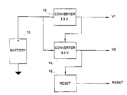
FIG. 1 iS a diagranl of a mixe~ ~ogic voltage level power supply systern.
FIG. 2 is ~ timing diagram of the subcircuit voltages in a mixed logic voltage ievel
power supply system.
FIG. ~ is an illustra~ion of the internal circl~itry arrangement in the reset subcircuitry
in a mixed logic volt2ge level power supply system.
1~ DESCRIPTION OF AN EXEMPLARY EMBODIMENT
FIG 1 depicts the power supply layout and the i"terconnection of the subcircuitry
for delivering power to the devices in a typical data tenninal computer sys~ern. The battery
10 ("BATTERY") is the main power source in a port~ble data terminal system, and is
~onnected to the input terrninals ~f the power converter 12 ("CONVERTER 3.3 V") for the
system ha~ware devices which operate at 3.3 volts and the power converter 14
("CONVERTER 5.0 ~') for the system hardware devices that operate at 5 0 volts. The
o~tput V1 o~ the 3.3 volt c~nve~tPr 12 supplies power at a 3.3 volt logic voltage level to the
hardware operatin~ at 3.3 volt logic levels The output V2 of the 5.0 volt converter 14
suppli~s pow6~ at a ~.0 volt logic level to the hardware operating at 5.0 volt logic levels.
2~ Additionally, the output ~r1 of the 3.3 volt converter 12 connects to the shutdown
pin of the 5.0 volt ~onvertGr 14 The output of the 5.0 volt convertar 14 connects to the
input o~ the RESET subcircuitry 16 ("RESEr'). The RESET subcircuitry 16 supplies a
~igital signal to the syste~n hardware devices for reinitiaiization of the lo~ical states. With
the power supply circuits arranged in tandem in the above d~scribed fashion, power is
~elivere~ sequentially to the system subcircuitry
2 1 62302
._ ! I
FIG 2 illustrates the timing of the order in which the Icgic voltage supply signals
power the systen~1 hardware. The vertical axis illustrates the increasing relati~e volt~e
levels for the pow~r supply subcircuits. The vertical axis represents the direction of
increasing v~ltage only, as the purpos~ of the diagram is to illustrate the timing sequence
5 o~ the individual s~lbcir~uits. The horizontal axis delineates the time at which switching of
the powering of the subcircuits occurs.
V1 represents the wave~orrn of the output of the 3.3 volt converte~ 12. Durin~ power
up, the 3.3 volt converter 1~ is the first subclrcuit to recei\~e power. The output of the 3.3
volt converter 12 increases over time ultimately reaching a nominal value of 3.3 volts.
uring the time which the 3 3 volt conYerter 12 is being powered up, the 5.0 volt converter
14 and the RE$ET 16 subcircuits recei\~e no power.
Referring backto FIG. 1, the output ~11 of the 3.3 volt converter 1~ conne~ts to the
shutdown pin of the 5.0 volt ~onverter 14. This arrangement causes the 5.0 Yolt con\Jertor
14 to remain off even though there is a power signat connected to the input terminal of the
1~ 5.0 volt conYerter 14. Further, the 5.0 volt converter 14 supplies the power for the RESET
subcircuitry 16, and therefore the RESET subcircuitry 16 will not send a RESET si~nal until
it receives power frcm ~he 5.0 volt converter 14. Correspondingly, the output V2 from the
5.0 volt converter 14 and the RESET 16 subcircuits during the power up of the 3.3 volt
converter 12 is z~ro. Thus, in an exemplary em~odiment, the system h~rdware operating
20 at 3.3 volt logic levels is powered up before any other system hardware.
The output voltage V1 cf the 3.3 volt converter 12 rises until it reaches a voltage Vg1
sufficient to tlJrn on the 5.0 volt converter 14. In an exemplary ernbodiment V~1 is
approximately 3.0 volts. This occurs at a time t1, ~t which time the output voltage V2 of the
~.0 volt converter 14 be~ins to rise as the 5.0 voll converter 14 is powered up. The o~Jtput
2~ voltage of the 5.0 volt converter 14 increases until it reaches a volt~ge Vg2 sufficient to
power the RES~T su~circuitry 16. Thi~ occu~s at tirne t2, ~t which time the RESET
subcircuitry 16 begins to re~eive power. The output of the RESET subcircuitry 18 occurs
after a time delay of ~ resultin3 from the charge time of the internal RESET subcircuitry 16.
The output voltage of the RESET subcircuitry 16 is the RESET digital signal for
2 1 6230~
.~ .
reinitialization of system ha~ware. System hardw~e cannot be reinitialized until the 5.0
volt hardware receives power. I
Thus, the o~cler in which the system hardware recei~r~s power is as follow$;
1. The battery delivers p~wer to the power supply converters;
2. The 3 3 volt hardwark is powered up;
3. The 5.0 volt har~ware is powered up;
4. The reset circuitry is powered up;
5. System hard~are is reinitialized.
Fl~. 3 depicts the internal circuitry of the RESET subcircuitry 16. The output V2 of
the 5.0 volt converter 14 supplies the power for the RESET subcircuit 16. Th~ power
supply input V2 of the RESET subcircuit 1~ connects in sefies to a resistor 18 ("R") which
further connects to a capacitor 20 ("C"), such node being the RESET output signal of the
RESET subcircuitry 16. The ~athode of a diode 22 in connected in pa~allel with the
capacitor Z0 also connects to the output node. A pushbutton reset switch 24 connects in
parallel with the diode 22 and the capacitor 20. The pushbutton reset switch 24 allows for
manual reinitialization of system ha~ware.
The capacitor Z0 and the resistor 18 determine the RESET signal delay time ~l
which is the delay from t21 ~hen the 5.0 volt co~verter 14 is powered up, to the time at
whieh the RESET subcircuitry 16 may send a RESET signal. The delay time I is
20 determined by the following relation;
~ = RC
The time delay ~ of the RESET subcircuit 16 ensures th~t the RESET signal will not be
25 asserted high until aftef the 3.3 volt hardware and the 5.0 volt hardware receive power.
Thusl in an exemplary e~,bodil"entl the RESET si~nal is always ~sserted low whenthere is no signal available from the 5.0 volt converter 14. Addi~ionally, the RESET signal
is not asserted high unless the output signal V2 of the 5.0 volt conYer~er 14 is present at
~ 2 1 62302
.
the input of the RESET subcircuit 16, even when the pushbutton res~t switch 24 is
depressed.
In an altemative embodiment, the aforementioned power supply and accompanying
cir~uitry may be mounted in ~ self-contained battery p~ unit. A self-contained b~ttery
5 pack arrangement of the herein disclosed invention allows for e~nployment of the invention
in currently existing mixed logic voltage computer systems such that these currently
existing systems may obtain the adYantages of the invention without the need for redesign
of these systems. Additionally, any future redesi~n or other irnprovements of the existing
invention may be irnplemented without signi~icant redesi~n of the preexistir)g computer
10 systems, thereby reducin~ costs associated therewith.
~ hus, there has been described a power supply system in a mixed lo~ic voltage
compute~ system that achieves the ob~ect of delivering power tc the system hardware
subcircuitry in a sequence based upon the logic voltage levels at which the particular
devices of the subciru~itry operate in ~rder ~o minimize startup power consumption.