Note : Les descriptions sont présentées dans la langue officielle dans laquelle elles ont été soumises.
--- Wo s4/26sso 21~ 2 ~ 7 :~ PCT/US94/03059
METALLIC FILMS AND ARTICLES USING SAME
Field of the Invention
This invention relates to metallic films and articles using such metallic
films to advantage.
Back~round of the Invention
U.S. Pat. No. 4,257,424 (Cartmell) discloses that the use of a vacuum
deposition of silver proves to be undesirable because vacuum deposited silver is not
securely retained by a substrate such as Mylar.
U.S. Pat. No. 4,848,348 (Cr~ighe~) discloses the deposition of silver
on a primed surface of an organic film. The primer is comprised of binder and
powder particles, which was prefell~d to using a plasma treated film.
U.S. Pat. No. 3,255,099 (Wolinski) discloses the use of corona
treatment at atmospheric pr~s~ur~ as a priming method for organic films. Among
inorganic agents used is hydrogen sulfide.
Japanese Patent Publication 61-59,526 discloses the deposition of H2S
at a 200 Angstrom thickness on a surface.
Summary of the Invention
The present invention overcomes the disadvantages of the prior art by
providing a metallic film comprising a subsL,dte of organic polymer, a sulfur-reactive
surface on the organic polymer substrate, and a metallic layer adhered to the organic
polymer surface via sulfur-metal interaction.
"Sulfur-reactive surface" means that the surface of the organic polymer
substrate has become reactive due to the presence of a composition having a sulfur
functionality.
One embodiment of the present invention is use of a sulfur-cont~ining
compound, e.g., barium sulfate, in the bulk of the organic polymer substrate, such
7 3
wo 94/26950 - PCT/US94/03059
that a metallic layer is adhered to the surface of the organic polymer substrate with
greater adhesion than such adhesion in the absence of such sulfur-cont~ining
compound.
Another embodiment of the present invention is the use of a sulfur-
5 cont~ining compound, e.g., hydrogen sulfide reacting with the surface of the organicpolymer substrate to provide the surface with that sulfur functionality.
A third embodiment of the present invention is the use of sulfonated
organic polymer substrate surface, i.e., sulfonated polyester.
"Sulfur-metal interaction" means covalent bonding or coordination
10 bonding, or a combination of both, depending on the type of composition having
sulfur functionality and the type of metallic layer employed.
The presence of the sulfur functionality on the organic polymer
substrate is used according to the present invention to improve adhesion of a metal,
e.g., silver, to the substrate.
According to the first embodiment of the present invention, the organic
polymer substrate is modified by mixing into such polymer, during or after
formation, a sulfur-cont~ining co"-pound which is reactive with a metal when themetal contacts surfaces of the substrate during vapor deposition thereof.
According to the second embo~im~nt of the present invention, the
20 organic polymer substrate is modified by eAI OS.I~ of the surface(s) of the substrate to
a vacuum glow discharge or plasma. The gas in which this plasma is created
comprises a sulfur-cont~ining cGI-~pound. The reaction between the organic polymer
and the plasma-delivered sulfur~nlAining co...poulld produces an organic-sulfur
surface having carbon-sulfur covalent bonds.
The sulfur-reactive surface is a priming surface for reaction of a metal
to adhere to such primed surface via metal-sulfur interaction.
A feature of the invention is the ease and perm~nence of formation of a
metallic film using a sulfur-reactive surface, primed for metal-sulfur interaction with
a vapor deposited metal.
Another feature of the invention is the use of an sulfur-reactive surface
to form a coordination or covalent bond with the metal layer, such as silver.
An additional feature of the invention is ability to form an extremely
thin, vapor-coated, precious metallic layer on an organic polymer substrate having
--- wO 94/26950 21 6 2 ~ 7 3 PCT/US94/03059
acceptable or superior functional pr~pellies. This ability can minimi7e e~l~"sf in
production of metallic films when using precious metals to form films.
- An advantage of the invention is the çlimin~tion of the use of a
metallic ink in the formation of a metallic film. An ink is dependent on metallic
5 particle size, proper binder selection and usage, and often ,~uires high coating
weights to achieve accept~hle conductivity. Hence, a met~ c ink having an
excessively high coating weight yields a met~llic film which is excessively radio-
opaque for biomPAiç~l electrode usages during m~Aic~l ima~ing procedures.
Another advantage of the invention is the use of simple, unfabricated
m~-~llic stock, such as metal pellets, that can be vaporized for application to the
sulfur-reactive primed surface of an organic polymer substrate. Vacuum deposition
of such metal assures a very thin uniform surface to establish acceptably high
conductivity and minimi7~ radio-opacity to achieve at least radiolucency and possibly
radiotransparency. Also, use of vacuum deposition of metal optimizes purity of the
metallic coating.
Another advantage of the present invention is that the priming of
organic polymer sul)sl,dtes minimi7~s del~min~tion of metal from the film and
reduces corrosion. In the emb~liment~ of the present invention, it has been found
that using the sulfur-reactive surfaces of the present invention to vapor deposit metals
achieves such adhesion that cohesive failure of the organic polymer subst~nti~lly
occurs prior to adhesive failure of the met~llic layer to the organic polymer substrate.
Another advantage of the present invention is the minim~l use of
expensive conductive metals, such as silver, without co",~ l-ising conductivity of
the metallic film so made.
The present invention also comprises a biomeAic~l electrode
comprising an electrical conductor, a field of ionically conductive medium having an
area with a perimeter contacting the electrical conductor to define an edge, anda layer of non-conductive material cont~tin~ the field of ionically conductive
medium and the electrical conductor and having an opening through which the field
of ionically conductive medium is exposed, wherein the layer of non-conductive
material covers the perimeter of the ionically conductive medium and the edge.
For a greater appreciation of the invention, embo~im~nts of the
invention are described after a brief description of the drawing.
2:~62~73
WO 94/26g50 PCT/US94/03059
Brief DescJi~lion of the Drawin~
FIG. l is a cross-sectional view of a m~t~llic film of the present
invention.
FIG. 2 is a top plan view of a biom~ic~l electrode cont~ining a
S biom~Aic~1 electrical conductor of the present invention, used for di~gnosi~ of heart
conditions of a m~mm~ n patient.
FIG. 3 is a cross-sectional view of the biomedical electrode of FIG. 2.
FIG. 4 is a pe,~pec~ive view of a moni~oling biomedical electrode
containing a biomedical electrical conductor of the present invention, used for longer
term diagnosis of heart conditions.
FIG. 5 is a cross-sectional view of the monilo~ g biomedical electrode
of FIG. 4.
FIG. 6 is a pe.~ec;Live view of a monitoring-defibrillation biomedical
electrode used for monitoring of heart conditions and the defibrillation of hearts in
emergency conditions with the release liner removed.
FIG. 7 is a cross-sectional view of the monitoring-defibrillation
biomedical electrode of FIG. 6.
Embodiments of the Invention
Or~anic Polymer Substrate
Organic polymers useful as ~,~bslldtes are those which can be
fabricated in the form of thin films for a variety of met~llic film usages. Non1imiting
examples of organic polymers are polyolefins, polyesters, fluorinated polyolefins
(e.g., polytetrafluoroethylene), and polycarbonates. If using more fully, fluorinated
polyolefins, a pre-tre~tment to remove at least some fluorination is necçc~.~.
Among these organic polymers, polyesters are prefGllGd for their known utility.
Among polyesters, polyethylene terephsh~l~tes are most p,ere,l~d. The
organic polymer can have any thicltne-ss acceptable to the u1tim~te usage.
For use as conductors in biomedical electrodes, the thickness of the
organic polymer as the substrate ranges from about 6 ~m to about 500 ~m.
Desirably, the thickness ranges from about 25 ~m to about 250 ~m. Preferably, the
thickness ranges from about 25 ~m to about 175 ~m.
~- wo 94~26gs0 2~ ~ 2 ~ 7 3 PCT/US94/03059
For use as window films, the subs~l~te thickn~cc ranges from about 4
~m to about 600 ~m. Desirably, the thit~kn~cc ranges from about 20 ~m to about 250
~m. Preferably, the thickness ranges from about 25 ~m to about 175 ~m.
For use as optical reflectors, the substrate thickne$s ranges from about
4 ~m to about 600 ~m. Desirably, the thick~ess ranges from about 20 ~m to about
250 ~m. Preferably, the thicknPss ranges from about 25 ~m to about 175 ~m.
For use in flex circuitry, the ~ubsl,~te thi-~nesc ranges from about 4
~m to about 600 ~Lm. Desirably, the thickness ranges from about 20 ~m to about 250
~m. Preferably, the thickness ranges from about 20 ~m to about 200 ~m.
Optionally, the organic polymer substrate can be prepated for sulfur
priming by employing the technique known as fl~chl~mp tre~tmPnt, such as that
disclosed in U.S. Pat. Nos. 4,822,451 and 4,879,176 (both Ouderkirk et al.), for use
with semicrystalline polymers. Fl~chl~mp treatment is known to provide an quasi-amorphous micr~,sulrace on a polyester substrate. Preferably, the organic polymer
substrate can undergo the fl~chl~mp treatment under conditions disclosed in the
patents identified above in order to better prepale the surface of the organic polymer
substrate for plasma genel~tion of the sulfur-reactive surface, with enhanced
adhesion, according to the second embodiment of the present invention.
Sulfur-reactive Surface
In the first embo iim~nt of the present invention, it is known that the
mixture of a sulfur-containing colll~ui1d into the bulk of an organic polymer
substrate as a filler improves cohesive strength of, or provides opacity for, the
polymer composite. Unexpectedly, such sulfur-conl;1ining compound also provides an
adhesion of the metallic layer that is superior to the adhesion provided by a polymer
substrate without such sulfur-cont~ining compound mixed therein.
The me~h~nicm of such increased adhesion is not completely known.
Without being limited to a particular theory, it is believed that the sulfur-con~ g
compound provides a sulfur-reactive surface to which metal can adhere using metal-
sulfur interaction.
Organic polymers having sulfur-cont~ining compounds are
commercially available, such as ICI 329 and ICI 339 "Melinex" branded polyester
films commercially available from ICI Americas of Hopewell, VA, that contain
7 ~
wo 94/269s0 PCT/US94/03059
barium sulfate as a filler therein.
In the second embodiment of the present invention, the surface of the
organic polymer substrate, (preferably rendered quasi-amorphous using a fl~hl~mptreatment), is primed with a sulfur~or.li~ini~-g co---Lo~nd to produce an organosulfur
5 surface.
The organosulfur surface is formed by a plasma-in~uc~d reaction of the
organic polymer with a sulfur-cont~ining gas or vapor. Nonlimiting examples of
sulfur-cont~ining compounds are alkyl llelc~ nc~ hydroxyalkyl -lel~aplans,
hydrogen sulfide, alkyl sl-lfides, carbon disulfide, and other sulfide gases.
10 Preferably, the sulfur-cont~ining compound is hydrogen sulfide gas.
The sulfur-cont~ining compound is reacted with the organic polymer
surface using a vacuum glow discharge or plasma in a chamber at l,lessu~s
significantly below atmospheric ple~ul~s, unlike those reaction conditions employed
in corona treatment techniques. The reaction between the organic polymer surface15 and the sulfur-cont~ining gas or vapor in the plasma produces an organosulfur surface
having carbon-sulfur covalent bonds. Thus, an organosulfur surface is uniformly
formed as a primer surface for reaction with metal according to the present invention.
In the third embo lim~nt of the present invention, a sulfonated surface
layer can be p~ d by flood coating an aqueous dispersion on an organic polymer
20 substrate according to techniques known to those skilled in the art. Such techniques
are described in U.S. Pat. No. 4,052,368 (Larson). A commercially available
polymer having a sulfonated surface is "Hoechst" SA polyester film from Hoechst
Chemicals.
The sulfur-reactive surface is thin, but can be controlled depending on
25 the type of surface provided and the embodiment of the invention employed. The
sulfur-reactive surface can be continuous or discontinuous, depending on the
thickness of the sulfur-reactive surface and depending on the embodiment of the
invention employed.
When using the first embodiment of the present invention, the presence
30 of sulfur-containing compound in the bulk of the organic polymer provides sulfur
functionality at the surface of the substrate. The surface is discontinuous due to the
particulate nature of the sulfur-con~ining compound in the bulk of the organic
polymer substrate.
~- wo 94/26g50 216 2 4 7 3 PcTlus94lo3os9
When using the second embodiment of the present invention, the
surface modified by sulfur functionality is preferably on the order of a few
nanometers thick. The surface can be continuous or discontinuous. As measured byXPS (ESCA), the organosulfur surface formed in situ at the surface of the organic
S polymer ranges from a submonolayer which is diccofi~in~o--c to a continuous layer of
about 10 nm. Desirably, the surface modified by sulfur functionality ranges fromabout 0.5 nm (about a monolayer) to about 5 nm. Preferably, the modified surfaceranges from about 1 nm to 3 nm thick.
When using the third embodiment of the present invention, the
organosulfur surface thickness, after any orientation procP,ssing, ranges from about
0.1 ~m to 10 ~m. The surface can be continuous or discontinuous.
Metallic Layer
Metals useful for the present invention depend on the material
plopellies, (e.g., electrical conductivity) desired for resulting metallic film.Nonlimiting examples of metals include ch~ llium, titanium, nickel, copper, tin,indium, gold, and silver, and alloys of them, with silver ~,~felr~d for its optimal
conductivity. The metal is evaporated in a chamber at low ples~ es and deposited to
react with the sulfur-reactive surface to form metal-sulfur bonds, coordination bonds,
or both. Preferably when silver is used, XPS (ESCA) shows the formation of a
silver-sulfide bond.
The metallic layer can have any thicl~ness acceptable to the ultim~te
usage.
For use as conductors in biomedical electrodes used for defibrillation,
tissue pacing stimulation, or cardioversion where electrical signals are delivered to
m~mm~ls, the thickness of the metallic layer ranges from about 100 nm to about 650
nm and preferably ranges from about 300 nm to about 500 nm. For use as
conductors in biomedical electrodes used for diagnostic or Illoniloling procedures
where electrical signals are received from ",~."...~lc, the thickness ranges from about
50 nm to about 300 nm and preferably ranges from 100 nm to about 250 nm.
For use as window films, the thickness ranges from about 0.5 nm to
about 600 nm. Desirably, the thickness ranges from about 2 nm to about 25 nm.
Preferably, the thickness ranges from about 10 nm to about 13 nm.
~ ~162473
Wo 941269s0 PCT/US94/03059
For use as optical reflectors, the thickness ranges from about 10 nm to
about 1000 nm. Desirably, the thickness ranges from about 15 nm to about 300 nm.Preferably, the thickness ranges from about 20 nm to about 200 nm.
For use in flex cir~ ly, the thickness ranges from about 10 nm to
about 50 ~m. Desirably, the thickn~ss ranges from about 30 nm to about 30 ~m.
Ple~.dbly, the thi~n~s ranges from about 100 nm to about 10 ~lm.
These thickness ranges are broad in that various applications can utilize
metallic layers identified at opposite eAll`~llleS of the identified ranges.
Optional Metallic Halide Layer
In certain uses, particularly as conductors in biomedical electrodes, an
optional metallic halide layer is desirably added to or formed on the exposed surface
of the metallic layer. Of the halides useful, chloride is p~felled. Preferably, the
same metal is used in the metal halide as used for the met~llic layer. A metallic
halide layer interacts with the metallic layer to depolarize the metallic film following
high voltage, high amperage defibrillation of a patient. Bion~edic~l electrodes that
are capable of quick defibrillation recovery are strongly desired by health carepractitioners.
For use as conductors in biomedical electrodes used for defibrillation
or stimulation pull~oses, the thickness of the metallic halide layer ranges from about
100 nm to about 900 nm and preferably from about 500 nm to about 700 nm. For
use as conductor in biom~lic~l electrodes used for diagnostic or monitoring purposes,
the thickness ranges from about 5 nm (to provide a disconlinuous layer) to about 300
nm and preferably 80 nm to 150 nm.
Method of P~epal;,~ Sulfur-reactive Surface
In the first embodiment of the present invention, the organic polymer
is mixed either before or during polymerization with a sulfur-cont~ining compound
such as barium sulfate. Commercially available polyester films have been described
above and are especially useful to avoid substrate prep~lion.
In the second embodiment of the present invention, the sulfur-reactive
surface comprises an organosulfur surface.
In the third embodiment of the present invention, the sulfonated surface
~~ Wo 94/269s0 ;~ ~ ~i 2 ~ 7 3 PCT/US94/03059
is pl~ared according to the techniques described above.
In the plerelled second emb~YlimPnt, the organosulfur surface is
prepared by the exposure of organic polymer substrate surface(s) to a vacuum glow
discharge or plasma. The gas in which this plasma is created is a sulfur-co~-t~inillg
S colllpound, preferably hydrogen sulfide.
P,~sen~ly p~efelled reaction conditions for plasma reaction of the
sulfur-containing compound are a voltage of about 4-10 kV, an amperage of about
0.04-0.08 A/m width of substrate being treated at 0.15 m/sec, a gas flow rangingfrom about 70 to about 700 sccm (0.08 to about 0.75 g/m2 of substrate being
treated), and a line speed of about 10 to 300 mm/sec. Also for plasma reaction,
electrode to substrate spacing is about 10-30 mm, and a chamber pres~ule is fromabout 0.7 Pa to 12 Pa for the range of electrode spacings. Also ch~mher pres~llre of
2 and H2O should be minim~l and preferably less than 1 X 10⁻² Pa. The electrodes
are tubular and can be made from stainless steel, or preferably titanium, and are
15 cooled by using airflows or water through tubular structure of the electrodes.
The plasma-induced reaction of the sulfur-containing gas to the
substrate surface results in the formation of an org~nosulfur surface on the substrate.
XPS (ESCA) analysis reveals that covalent organosulfur bonds are formed at the
surface of the organic polymer.
This organosulfur surface is a priming surface for vapor deposition of
the metallic layer.
Method of Pr~p~in~ Metallic Layer
The metallic layer is formed by e~a~ldlive deposition in vacuum of a
metal on the sulfur-reactive, and pr~felably or~nos~-lfur, surface of the substrate.
Nonlimiting evaporation techniques known to those skilled in the art include heating
methods, (e.g., resistive, inductive, and electron beams,) and other physical vapor
deposition techniques (e.g., spull~ling).
Chamber pressure Of 2 and H2O used in metal deposition depends on
the metal selected for vapor deposition due to the tendency of the metal to oxidize.
When the metal is silver, the pressure Of 2 and H2O can be up to about 7 X 10⁻² Pa.
WO 94/269s0 ~ 1 6 2 4 ~ ~ PCTJUS94/03059
Method of Plc~)~;n~ Optional Metallic Halide Layer
The optional mçt~llic halide layer can be formed directly from the
metallic layer or can be a separate deposition step. When formed in situ, nonlimiting
techniques include chemical or electroc-hçmir~l oxidative chlorination.
Nonlimiting deposition techniques include evaporation in a vacuum
using resistive or inductive heating techniques; or solution deposition from aqueous
solutions of metallic halides, such as silver chloride.
With multiple layering techniques described, it is possible to combine
the method steps into a single pass within a vacuum chamber, such that in a plcfellcd
embodim~nt, hydrogen sulfide treatment, and silver and silver chloride deposition can
be sequentially pclÇo-"-ed on the surface of an organic polymer substrate.
Preferably, this organic polymer substrate has been previously p~cpalcd with a
fl~shl~mp treatmçnt according to the method described above.
Usefulness of the Invention
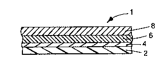
FIG. 1 shows a metallic film 1 of the present invention. The substrate
2 has an sulfur-reactive surface 4, (preferably an organosulfur surface) formed
thereon, to which a met~llic layer 6 is deposited. Optionally as shown, a metallic
halide layer 8 is deposited on the metallic layer 6.
Biomedical Electrodes
Biomedical electrodes employing metallic films of the present invention
as biomedical electrical conductors are useful for diagnostic or monitoring purposes,
for transcutaneous electrical nerve stimulation (TENS) pLlll)O~;S~ defibrillation,
cardioversion, tissue pacing stimulation, or as a electrical dispersive plate for
electrosurgery. In its most basic form, a biomedical electrode is a tr~ncduc~r that
converts electrical current to ionic current or vice versa. I~inim~lly, the electrode
comprises an ionic~lly conductive medium c~nt~rting skin and a means for electrical
communication interacting between the ionically conductive medium and biomedicale~uipment.
FIGS. 2 and 3 show either a disposable diagnostic electrocardiogram
(ECG or EKG) electrode 10 or a TENS electrode 10 on a release liner 12. Electrode
10 includes a field 14 of a biocompatible and adhesive ionically conductive medium
-10-
~- wO 94/26950 ~ 2 4 7 3 PCT/US94/03059
for cont~ting skin of a patient upon removal of protective release liner 12.
Electrode 10 includes means for electrical communication of the present invention
comprising a biomedical electrical conductor 16 having a conductive interface portion
18 contacting field 14 of ionically conductive medium and a tab portion 20 not
- 5 contacting field 14 of ionically conductive medium for mech~ni~l and electrical
contact with electrical equipment (not shown). The tab portion 20 can be arcuately
slit (not shown) in an arc of about 120 to about 270 having a radius of about 2 mm
to about S mm in an internal area of the tab for more assured com1e~;1 ion with
gripping extension of the electrode clip.
Conductor 16 is shown in a multi-layered construction (similar to that
shown in FIG. 1) of a nonconductive, flexible polymeric film substrate 24 having an
sulfur-reactive surface 25, a metallic layer 26 deposited on and interacting with the
surface 25, and an optional metallic halide layer 28. The conductive interface portion
18 of member 16 comprises a metallic layer 26 deposited on an sulfur-reactive
surface 25 on at least the side of polymeric film substrate 24 facing field 14 of
conductive medium and the optional metallic halide layer 28 coated on the metallic
layer 26 and contacting field 14. Re~use depolarizing is not needed for the
mechanical and electrical contact with electrical equipment, optional metallic halide
layer 28 does not need to extend to tab portion 20.
It is foreseen that a typical EKG conductor member 16 be thin and
flexible. Polymeric film substrate 24 typically has a thickness ranging from about 20
~m to about 150 ~m, and prc:reldbly has a thickness of about 75-100 ~m.
When used for ~i~gnostic, monitoring, or TENS pullJoses, metallic
layer 26, as a vapor deposited layer, has a thickness ranging from about 80 nm to
about 100 nm. When used for defibrillation, tissue pacing stimulation, or
cardioversion, metallic layer 26 has a thickne~ from about 100 nm to about 300 nm,
and preferably has a thickness of about 200 nm to achieve at least 50 defibrillation
pulses.
When used for diagnostics, monitoring, or TENS pUl~oS~s, optional
metallic halide layer 28, when vapor deposited, has a thickness ranging from about
100 nm to about 350 nm, and preferably a thickness of about 200 nm. When used
for defibrillation, tissue pacing stimulation, or cardioversion, optional metallic halide
layer 28 has a thickness from about 500 nm to about 700 nm and preferably about
WO 94/26950 216 ~ ~ 7 3 PCT/US94/03059
600 nm.
Presently pr~fe,lcd for polymeric film substrate 24 are polyester films
such as "Scotchpar" commercially available from Minnesota Mining and
Manufacturing Company of St. Paul, MN or "Melinex" ICI 329, or ICI 339 film
5 from ICI Americas of Hopewell, VA.
I~e~nlly pr~re"cd for met~llic layer 26 is vapor deposited silver.
To enh~noe mto.ch~nic~l contact between an electrode clip (not shown)
and tab portion 20 of conductor member 16, an adhesively-backed polyethylene tape
can be applied to tab portion 20 on the side opposite side 22 having the electrically
10 conductive layer 26. A surgical tape commercially available from 3M Company as
"Blenderm" tape can be employed for this purpose.
For the conductive medium 14, ionically-conductive gels and adhesives
are used. Nonlimiting examples of ionically-conductive pressure sensitive adhesive
compositions are solid state conductive polymer compositions disclosed in U.S. Pat.
Nos. 4,524,087; 4,539,996; 4,554,924; and 4,848,353 (all Engel); EPO Publication0 322 098 (Duan); EPO Publication 0 542 294 Al (Uy et al.); and adhesives
disclosed in U.S. Pat. Nos. RE31,454 (Hymes); 4,391,278 (C~h~l~n); 4,699,146 and4,750,482 (both Sieverding).
Another type of di~gnostic procedure which can employ a biomedical
electrode of the present invention is the longer term monilo,ing of electrical wave
~Ut;llls of the heart of a patient to detect patterns of abnormality. A p~fe"ed
biomedical electrode structure is disclosed in U.S. Pat. No. 5,012,810 (Strand et al.).
The mes~llic film of the present invention can be used as the conductor member in
any of the embodiments shown therein. Preferably, the m~t~llic film of the present
invention is used as the biomedical electrical conductor in the biome~ l electrode of
the embodiment shown in Figs. 2, 3, and 4 of U.S. Pat. No. 5,012,810.
Figs. 4 and 5 substantially co"e~l,ond to Figs. 2 and 3, respectively,
of U.S. Pat. No. 5,012,810. Electrode 40 includes an incul~tor construction 41, and
a conductor member 42.
The in~ul~tor construction 41 includes first and second sections 44 and
45 which, together, define opposite sides 46 and 47 of the in~ul~tor construction 41.
As seen in Fig. 5, each section 44 and 45 includes an elongate edge portion 50 and
51, respectively. The edge portions 50 and 51 each include a border portion 52 and
--- WO 94/26950 2 ~ 6 2 4 7 3 PCT/US94/03059
53, lespecli./ely, which comprise a peripheral portion of each section 44 and 45,
e~ ely, and exten-ling along edges 50 and 51, l~,s~ ely. In that manner,
sections 44 and 45 are oriented to extend ~ubsl~r~L;~lly parallel to one another, with
edge portions 50 and Sl overlapping one another such that border portions 52 and 53
S overlap. A seam 60 is created between edge portions 50 and 51. "Subst~nti~lly
parallel" does not mean that the sections 44 and 45 are ne~es~rily precisely parallel.
They may be out of precise coplanar ~lignm~nt due, for example, to the thickness of
the conductor member 42.
Conductor membçr 42 is subst~nti~lly similar to biomedical electrical
10 conductor 16 described above, having a tab portion 61 corresponding to tab portion
20 described above and a pad portion 62 collt;sponding to conductive interface
portion 18 described above. Like biomedical electrical conductor 16, conductor
member 42 is a multi-layered construction of a nonconductive, flexible organic
polymer substrate 63 having an org~nos~-lfur surface 64, a metallic layer 65 adhered
15 thereto, and, optionally, a met~llic halide layer 66.
The pad portion 62 of m~mbçr 42 comprises the portion of the metallic
film facing field 70 of conductive adhesive, optionally with me~llic halide layer 66
contacting field 70. Rec~l-se depolarizing is not needed for the mechanical and
electrical contact with electrical equipment, metallic halide layer 66 need not extend
20 to tab portion 61. Optionally, an adhesively-backed polyethylene tape can be applied
to tab portion 61 in the same manner as that for the embodiment of Figs. 1 and 2, in
order to enh~nc~ ,-e~h~nical cont~ct
In general, electrode 40 is constructed such that tab portion 61 of
conductor member 42 projects through seam 60 and over a portion of surface or side
46. As a result, as seen in Pigs. 3 and 4, pad portion 62 of conductor member 42 is
positioned on one side 47 of ins -l~tor construction 41, and the tab portion 61 of
conductor member 42 is positioned on an opposite side 46 of in~ul~tor construction
41. It will be understood that except where tab portion 61 extends through seam 60,
the seam may be sealed by means of an adhesive or the like.
As seen in Fig. 5, lower surface 68 of tab portion 61 is shown adhered
in position to section 45, by means of double-stick tape strip 69. That is, adhesion in
Fig. 5 between the tab portion 61 and section 45 is by means of adhesive 69
underneath tab portion 61, rather than on top as shown in Fig. 4.
-13-
Wo 94/269s0 2 ~ 6 2 4 7 3 pcTlus94lo3os9
In Fig. 5, a field 70 of conductive adhesive is shown positioned
generally underneath conductive member 42. Usually, field 70 of conductive
adhesive will be surrounded by a field 71 of skin adhesive also applied to incul~tor
construction 41 the side thereof having pad portion 62 thereon.
In Fig. 5, a layer of release liner 75 is shown positioned against that
side of electrode 40 which has skin adhesive 71, conductive adhesive 70 and pad
portion 62 thereon. Optionally as shown in Fig. 5, a spacer 76 or tab 76 can be
positioned between release liner 75 and a portion of incnl~tor construction 41, to
facilitate the separation.
A variety of release liners 75 may be utilized; for example, a liner
comprising a polymer such as a polyester or polypropylene material, coated with a
silicone release type coating which is readily separable from the skin adhesive and
conductive adhesive.
A variety of materials may be utilized to form the sections 44 and 45
of the ins~ tor construction 41. In general, a flexible material is p~erelled which
will be comfortable to the user, and is relatively strong and thin. Plerelled materials
are polymer foams, espe~islly polyethylene foams, non-woven pads, especially
polyester non-wovens, various types of paper, and transparent films. Nonlimitingexamples of tl~1sl~arenl films include polyester film such as a polyester film
commercially available as "Melinex" polyester film from ICI Americas, Hopewell,
VA having a thickness of 0.05 mm and a surgical tape commercially available from3M Company as "Transpore" unembossed tape.
The most preferred materials are non-woven pads made from melt
blown polyurethane fibre, which exhibit exceptional flexibility, stretch recovery and
breathability. Melt blown polyulelhane materials usable in insul~tor construction 41
in electrodes according to the present invention are generally described in European
Patent Publication 0 341 875 (Meyer).
Preferably the incl-l~tor construction has a skin adhesive on its surface
contacting the remainder of the electrode 40.
Preferred web materials (melt blown polyurethanes) for use in inclll~tor
construction 41 have a web basis weight of about 60 140 g/m2 (preferably about 120
g/m2). Such materials have an applo~liate tensile strength and moisture vapor
tr~nsmicsion rate. A pferell~d moisture vapor tr~ncmiccion rate is about 500-3000
~~ Wo 94/26950 ~ 1 ~ 2 4 7 3 PCT/US94/03059
grams water/m2l24 hours (preferably 500-1500 grams water/m2/24 hours) when tested
according to ASTM E96-80 at 21C and 50% relative humidity. An advantage to
such materials is that webs formed from them can be made which exhibit good
elasticity and stretch recovery. This means that the electrode can stretch well, in all
5 directions, with movement of the subject, without loss of electrode integrity and/or
failure of the seal provided by the skin adhesive. Material with a stretch recovery of
at least about 85%, in all directions, after stretch of 50% is plefellt;d.
It will be understood that a variety of tlimPncions may be utilized for
the biom~dic~l electrode disclosed herein. Generally an inc~ tor construction ofabout 3.5-4.5 cm by 5.5-10 cm will be quite suitable for typical forc~l1
applications. A thickness of about 200 to 600 ~m provides for adequate strength and
a desired low relief or profile, in typical applications.
It will also be understood that a variety of materials may be utilized as
the skin adhesive. Typically, acrylate ester adhesives will be pr~felled. Acrylate
15 ester copolymer adhesives are particularly piefelled. Such material are generally
described in U.S. Pat. Nos. 2,973,826; Re 24,906; Re 33,353; 3,389,827;
4,112,213; 4,310,509; 4,323,557; 4,732,808; 4,917,928; 4,917,929; and European
Patent Publication 0 051 935.
In particular, an adhesive copolymer having from about 95 to about 97
20 weight percent iso-octyl acrylate and from about 5 to about 3 percent acrylamide and
having an inherent viscosity of 1.1-1.25 dl/g is plesenlly p~efell~d.
Adhesive useful as for adhesive 69 can be any of the acrylate ester
adhesives described above in double stick tape form. A presently pIefell~d adhesive
is the same adhesive as presently pref~l~ed for the skin adhesive except having an
inherent viscosity of about 1.3- 1.45 dl/g.
For the field 70 of conductive adhesive, conductive adhesives such as
those described above as useful for field 14 of conductive medium are prefelled. It
will be understood that the ~im~ncions of the various layers, and their conformation
during association, are shown somewhat exaggela~ed in Fig. 5, to facilitate an
understanding of the construction. In general, an overall subst~nti~lly flat ap~al~nce
with only a very minor "s" type bend in the conductive member 42 is accommodatedby the arrangement, despite the multi-layered construction of member 42.
Other examples of biomedical electrodes which can use the present
-15-
wo 94/26950 ~ 4 ~ 3 pcTlus94lo3oss
invention as biom~Aic~l electrical conductors include electrodes disclosed in U.S. Pat.
No. 4,527,087; 4,539,996; 4,554,924; 4,848,353 (all Engel); 4,846,185 (Carim);
4,771,713 (Roberts); 4,715,382 (Strand); 5,133,356 (Bryan et al.). Methods of
making such electrodes are disclosed in such patents, except that the biomeAic~l5 electrical conductor of the present invention can be substituted for the various means
of electrical communication disclosed in such patents. Among these various
electrode constructions is an electrode construction particularly prcÇcllcd as that
shown in FIGS. 4 and 5 of U.S. Pat. No. 4,848,353 (Engel) in which the
co"lbination of electrode plate 33 and polymeric b~c'~ing 34 is replaced by the
10 metallic film 1 of the present invention.
When used for diagnostic EKG procedures, electrodes shown in Figs.
2 and 3 or those electrodes shown in U.S. Pat. No. 4,539,996 are ~lcrerlcd. Whenused for monitoring electrocardiogram (ECG) procedures, electrodes disclosed in
U.S. Patent Nos. 4,848,353, 5,012,810 and 5,133,356 are plcrcll~d.
In some instances, the biomedical electrical conductor can be an
electrically conductive tab extending from the periphery of the biomedical electrodes
such as that seen in U.S. Pat. No. 4,848,353 or can be a conductor lllclllbcr
extending through a slit or seam in a in~ ting backing member, such as that seen in
U.S. Patent No. 5,012,810. Otherwise, the means for electrical communication can20 be an eyelet or other snap-type connector such as that disclosed in U.S. Pat. No.
4,846,185 with the depolarizing layer coated on a graphite coated snap electrode.
Alternatively, an electrically conductive tab such as that seen in U.S. Pat. No.5,012,810 can have an eyelet or other snap-type connc~;lor secured thereto.
Another embodiment of a biomedical electrode is shown in FIGS. 6
25 and 7. This biomedical electrode is suitable for both monitoring heart activity and
for initiating defibrillation, tissue pacing stimulation, and cardioversion procedures.
Electrode 80 comprises, in layers, a foam in~ ting layer 82 having a field 84 ofbiocompatible pressure sensitive adhesive covering one surface of the layer 82.
Within the periphery of adhesive field 84 is adhered a m~t~llic film 86 of the present
30 invention constructed in the same manner as for conductors 16 and 42, previously
discussed. At the periphery of metallic film 86 is a non-conductive layer 88 which
adheres to field 84 of adhesive and covers the periphery of film 86. Non-conductive
layer 88 has an opening in which a field 90 of conductive gel or conductive adhesive
-16-
216247~
--- Wo 94/26950 PCT/US94/03059
adheres to metallic film on the surface at the opening. The interface 91 away from
the opening is ~lut~cled with BlendermTM tape from 3M Company and the top of thefilm 86 wherein the connector is to be ~tt~hed. The opening is where the conductive
area is exposed. The non-conductive layer 88 also has bioco"~atible pressure
- 5 sensitive adhesive covering one surface, using adhesives described above with respect
to the electrodes seen in FIGS. 4 and 5.
The geometric shape of electrode 80 minimi7~s the presence of any
abrupt intersections of edges, such as cornèrs. Each of the coll-ponents of electrode
80, especially the metallic film 86, is shaped to avoid corners where the edge effect
of high voltage, and high wattage electrical power flux to skin can cause arcing and
electrical burns. It has been found that the substantially egg shaped metallic film 86
within electrode 80 minimi7~os arcing when contacting m~mm~ n skin.
Electrical connection from metallic film 86 to electrical instrumentation
(not shown) can use a metal-containing or metal-covered post 92 ~tt~-~Pd to the metal
film 86 and incul~ted from the outside between two foam layers 82 and 88.
It is a feature of this biomedical electrode of FIGS. 6 and 7 that the
conductive area of the electrode for tissue pacing stim~ ting, defibrillation, or
cardioversion is limited to that area of the opening as seen in FIGS. 6 and 7, such
that arcing and electrical burns caused during tissue pacing stimlll~tion~
20 cardioversion, or defibrillation are minimi7~d at the edge where the field 90 of
conductive gel or adhesive contacts mPt~llic film 86. Opening in layer 88 through
which field 90 is exposed is smaller in perimeter ~imencions than the perimeter edge
of field 90 contacting film 86. This diminution of surface area of field 90 is
overcome by the edge p~ote~;lion afforded for electrode 80 to minimi7e arcing and
25 edge burns.
Foam incul~ting layer 82 can be any non-conductive polymeric foam
material useful to those skilled in the art. Nonlimiting examples of such foam
materials are high density thin polyethylene foams. Presently p,efelled for layer 82
is 0.50 mm 8EO Volara polyethylene foam commercially available from Voltek of
30 Lawrence, MA.
Biocompatible l)res~ e sensitive adhesive useful for field 84 can be
any of the skin adhesives identified above. Plesently prefel,ed as an adhesive for
field 84 is 12 grains of a 91:9 isooctyl acrylate:N-vinyl-2-pyrrolidone copolymer
2~2473
WO 94/269s0 PCTIUS94/03059
pressure sensitive adhesive or 18 grains of a 94:6 isooctyl acrylate:acrylic acid
copolymer tackified with a "Foral" branded colophony acid rosin, such as "Foral
AX" or "Foral 85" resins commercially available from Hercules Corporation, present
in an amount of from about 35-40 weight percent of the copolymer solids.
Metallic film electrical conductor 86 can employ any con,bina~ion of
the organic polymer substrates, sulfur-reactive surfaces, metallic layers, and
optionally, metallic halide layers described above. Plesenlly preferred for metallic
film 86 is a 50 to 100 ~m thick polyester polymer substrate having a 1 nm thick
orp~noslllfur surface, a 450 nm thick vapor deposited silver layer, and a 650 nmthick vapor deposited silver chloride layer.
Non-conductive layer 88 can be any thin polymeric film that adheres
well to the field 84 of adhesive. Nonlimiting examples of thin polymeric films
include high density polytheylene foam. Presently p-efer.ed for layer 88 is the
Volara foam identified above.
Conductive gel or adhesive for field 90 can be any of the conductive
gels or adhesives previously identifie~ for conductive medium 14 or field 70 of
conductive adhesive. ~csently p~rel-~ for field 90 is an acrylic acid/N-vinyl
pyrrolidone copolymer conductive adhesive ~ osP~ in U.S. Pat. No. 4,848,353
cont~ining 3 weight percent of potassium chloride.
Post 92 can be any metallic piece with a mechanical connection
compatible with electrical instrl~ment~tion~ preferably nickel plated.
Nonlimiting examples of electrical instrumPnt~tion are defibrillation
equipment commercially available from Physio-Control Co,~lation, Hewlett
Packard Corporation, and Marquette Electronics.
A release liner 94, like liner 75 described above, can be used to
protect field 90 and foam 88 during storage from premature exposure to the
environment.
An advantage of biom~ic~l electrode 80 is that it is acceptably
radiolucent and can remain on a patient during radiographic procedures, such as
electrophysiology studies and radiotherapy procedures. Such procedures generallyuse about 75 kV peak, 6mA. An electrical conductor having a signific~ntly greater
thickenss than used here would be radiopaque and would appear in the image
produced by the radiographic procedure. X-rays above about 40 KeV, 300 mA do
-18-
--- Wo 94/26g50 21 ~ 2 4 7 3 PCT/US94/03059
not reveal a biomedical electrode image, notwithct~nr~ing the presence of a metallic
film of the present invention. The minimi7~tion of the amount of radiation absorbing
metal via vapor deposition permits acceptable radiolucency.
Window Films
S Window films employing metallic films of the present invention are
useful for window films which reduce solar radiation, glare, infrared radiation and
microwave radiation, or modify color of either reflected or tr~nsmined light. These
metallic films are applied to windows for various architectural and energy saving
reasons. Metallic films are app,opliate for application as window films include
silver, copper and alloys of copper such as copper-tin mixtures, indium and gold.
The metallic film are preferably semi-transparent, with luminous
tr~nsmi~ion ranging from 0.1 to 80%. Desirably, the luminous tr~nsmi~sion rangesfrom 2 to 70%, preferably 5 to 60% in typical applications. The dense, highly
adherent metallic films can provide metal films having reduced rates of corrosion,
which can be important for this application.
The polymeric substrate used for this application is preferably
transparent, scattering a minimum of light, precluding the use of filled films.
Optical Reflectors
Optical reflectors employing metallic films are useful for reflectors for
illumination systems and solar energy collectors. For both applications, corrosion
stability and adhesion are i,.,pol~nt pro~llies provided by metallic films of the
present invention.
Since reflectors are subs~ lly opaque, (e.g., less than 10% light
tr~ncmiC-sion~) subsl~ates may be filled and thus scatter light, so any one of the three
embodiments of the present invention may be ~sed to improve adhesion.
Metallic films of the present invention can be used in solar collectors
and reflectors in a manner according to U.S. Pat. Nos. 4,307,150 and 4,645,714
(both Roche).
Flexible Electronic Circuitry
Since flexible electronic circuitry is opaque, optical properties are
unimportant. Therefore, substrates may be filled and any one of the three
-19-
~I~273
Wo 94/269s0 PCT/US94/03059
embodiments of the present invention of the met~llic films may be used.
Metallic films of the present invention can be used in metal-clad
- dielectric sheeting in a manner according to U.S. Pat. No. 3,981,691 (Cuneo).
Metallic films can also be used in making printed circuitry in a ",anner according to
C~n~ n Patent 1,011,002 (Cuneo).
Metallic films of the present invention have particular advantage in
flexible electronic cirwit,y due to the low weight, high conductivity re~uirements in
compact electronic products such as notebook computers, watches, f~cimile
m~ ines, and other electronic products with minim~l space between electronicallyconnected modules.
Test Methods
Test Method I: Peel test
Two metho~s are employed to probe the adhesion of the deposited
15 silver coating to the polymeric substrate b~cking.
Test method A is a simple peel test con~i~ting of applying, with hand
pressure, a 20 mm wide by 75 mm long piece of ScotchTM brand Magic Tape
(manufactured by the 3M Col~,dtion, St. Paul, Minn.) to the metallic surface, then
rapidly remove, with a jerking motion, the tape at a peel angle of approximately20 120. Transfer of any silver from the substrate to the Magic Tape will constitute
failure according to this test method.
Test method B employs a specially manufactured test tape. 300 m of
50 ~m thick 220 mm wide polyimide film is coated with a 25% solids solution of
UNI-REZ 2645 thermoplastic polyamide adhesive resin (available from UnionCamp
25 Col~,dlion, Wayne, NJ) in a 70/30 toluene/propanol mixture. Coating conditions
are: 150 ~m wet coating, web speed 117 mm/sec, oven drying at 68C to 90C. A
25~m thick (dry) coating is produced. The coated film is converted into rolls of 100
m long 25 mm wide thermoplastic adhesive tape.
Strips of this thermoplastic adhesive tape (150 mm to 200 mm long)
30 are l~min~ted to the vacuum deposited silver surface of the test sample in either
cross web or down web direction. The l~min~ting conditions are: nip roll le"~ dture
126C, nip roll pressure 275 kPa (40 psi), l~min~ting speed 0.5 to 1.5 mm/sec.
After l~min~tion, the test sample is mounted in an Instron Tester
-20-
~162~7~
~~ Wo 941269s0 ~ PCT/US94/03059
Model 1122 (manura.;l~lred by Instron Co,~,dtion, Canton, Mass.) where the peel
force is measured (in grams/25mm width) at a 90 peel angle and at a speed of 5
mm/sec. In all, but the most severe cases, this procedure results in complete transfer
of the silver from the polymeric substrate to the peel tape. The measured peel force
- S (grams/25 mm width) thus provides a reproducible measure of the metal-polymer
substrate bond.
Test Method II: Coulometr c Deter~;r~tion of AgCl
On a piece of a heavy aluminum foil (150 mm by 150 mm) is extruded
a 5 mm thick coating of a solid conductive gel. The top surface of the gel is covered
with a polyethylene film to reduce evaporation. Through a slit in this film a given
area A of a silver/silver chloride coated conductor film is exposed to the conductive
gel surface. A 300 g weight with a basal area of 600 mm2 is placed on top of theconductor film to assure intimate contact with the gel surface. The negative terminal
of a precision DC power supply is conn~cted to the end of the conductor film
protruding through the slit in the polyethylene cover film. The positive terminal is
connectecl to the aluminum foil assuring a complete circuit. A silver/silver chloride
reference electrode is eAposed to the gel through a separate slit in the cover film. A
strip chart recorder and voltmeter is connected to the end of the con(~uctor film and
the reference electrode. When a current (from 3 to 9 mA) is passed through the
circuit a sharp voltage offset is observed when all silver chloride on the exposed area
of the conductor film has been converted to silver. At this point the current isinterrupted and the time recorded. The silver chloride coating t~ ness~ ~Ap~essed in
mC/cm2, can be determined from the time T(sec), The current I(mA), and the area
A(cm2):
t(mC/cm2) = [T x I]/A
Test Method m: AAMl Standard Electrical Testing
The AAMI Standards (Association for the Advancement of Medical
Instrumentation) for electrical testing of pregelled ECG disposable electrodes can be
found in Publication ANSI/AAMI EC12-1983. The Protocol calls for testing
pelrol..led on electrode pairs placed "back-to-back" with their conductive
adhesive/gel columns in contact with each other. Testing according to this protocol
2 ~ 7 3
WO 94/26950 PCT/US94/03059
was conveniently, and autom~tic~lly, carried out using a Xtratek model ET-65A ECG
Electrode Tester (manufactured by Direct Design,Inc., T f~neX~, Kansas).
Example 1.
In a Research type vacuum coater with a lS0 mm wide web drive
system was mounted a roll of 50 ~m thick polyester film (polyester tereph~h~1~te"ScotchParTMn manufactured by 3M Co-~lo,dlion, St Paul, MN). The chamber was
evacu~ted to a background pressure of l.33 x 10-5 Pa. A H2S glow discharge was
generated using a water cooled titanium electrode with a ground shield which directed
the glow towards the web. A flow of l l l sccm hydrogen sulfide, resulting in a
pressure of 2.7 Pa, a DC voltage of 5.0 KV and a current of 0.02 A was used for the
glow discharge. The web was treated at a speed of 20 mm/sec in a suspended state.
600 mm further along the web path the treated polyester was coated with a vacuumdeposited layer of silver achieving a surface conductivity of 2.5 S (norm~1i7~ per
squared length), an optical tr~n~mi~ion of O.l to 0.7 percent and a silver coating
weight of O. l mg/cm2. This co..~;~ponds to a silver coating thickness of 85 nm. Three
additional experiments were pelro-llled under varying glow discha-~e conditions in
Table l:
Table l
exp#~lye~t ~ 8tre~tmentcon~ition~8heet 8il~er 8ilver
ic~ne Q ronduct.~eight thic~-
~m H28flowVolt~g~urrent 8 mg/cm2 ne~s
~ccm) ~V A ~m
lA so111 5.0 0.02 2.5 0.1 85
lB 50111 5.0 0.02 1~.5-1~ 0.5 ~3
lC 50~2 3.8 0.06 7 0.16
lD 5018 3.5 0.03 13 0.56
The adhesion of the silver to the substrate was tested for samples lA to
30 lD using test method A as described above. Samples lA through lC passed this test,
whereas lD displayed occasional adhesion failure. A sample p~ ared as outlined
above for lA, but without the H2S glow discharge treatment, consistently failed the
silver adhesion test according to test method A.
-22-
~- WO 94n6950 216 2 ~ 7 3 PCT/US94/03059
EY~amPIe 2.
A sample was prepalod in similar fashion as example 1, except the silver coating had
a thickness of approx. 1 nanometer. The surface of this sample was analyzed using
XPS (ESCA). An XPS survey spectrum was recorded of the film surface and, from
5 this ~cllulll, the following relative surface el~omPnt~l composition was calcul~t~d:
Atomic % concentration
C O Ag S Si
59 18 1 1 4.8 7.5
The analysis showed the presence of Ag, S, and Si in addition to the base polyester
(C, O). The binding energy observed for the Si(2p3n ln) photoelectron peak indic~t~d
that the silicon was present as a silica type species and thus stemming from the slip
agent present on the surface of the PET film. Peak fitting the S(2p3n l'2) photoelectron
15 spectrum showed two distinct types of sulfur p-esent;
S(2p3'2) Binding Peak % of Total
energy (eV) ~ssignment Sulfur
161.75 Ag2S 57%
-163.62 Ag-S-PET 43%
25 This analysis demonstrated the p~s~nce of "organic" sulfur covalently bound to both
the silver coating and the PET film. The strong presence of the C(ls'n) peak in the
spectrum, evidence of the PET surface itself, suggested that the "organic sulfur"
containing layer was thinner than the ESCA analysis depth (~ 8 nm)
30 FY~mple 3.
Samples were p-epared as described in example 1 using 150 mm wide
100 llm thick PET (ScotchParTM). The conditions of the H2S treatment were varied,
and the resulting adhesion of the silver layer measured using peel test method B. The
results are indicated in the table 2:
WO 94/269~,0 ~ ~ 6 ~ ~ 7 3 PCT/US94/03059
Table 2
I128 Pri~er Con~ition ~ro~ ~e~ Dow~
E eel foroe web
a~p. , , gr~m~eel forc
128 flo~olt~g~;ul~e~ ebTomp~rob8peec~ 25mm gr~m-~/
~ccm) I~V A C ~m/~ec 25 mm
3A 100 6.60.0~5 ~0 12.5 102
3B 100 7.10.0~5 66 12.5 132
3C 85 7.10.020 ~6 12.5 198 202
3D 85 7.10.020 51 12.5 195 197
3}3 85 7.10.020 56 8.0 1~2 188
3F 75 7.10.015 53 10.0 186 167
3G 85 7.10.030 53 17.5 212 215
3H NoH28tre~tment (control) 59 ~7
15 FY~mrle 4
Several pieces of material lD from Example 1 were subjected to the
following treatment in order to produce a AgCI surface:
a) A 1% bleach solution (Hi-lex commercial household bleach) was
20 coated on the surface with a #6 Meier bar, followed by overnight drying at ambient
conditions
b) A 2% aqueous NaClO2 solution was coated on the silver surface
with a #6 Meier bar. After 5 min at ambient conditions the coating was rinsed with
25 water and air dried.
c) A Ag/AgCI ink solution (Ercon R-300 commercially available from
Ercon of Waltham, MA), at 50% dilution, was coated on the surface with a #6 Meier
bar followed by overnight drying at ambient conditions.
d) A 0.5% AgCl in aqueous ammonium hydroxide was coated on the
surface with a #6 Meier bar, dried at ambient conditions for 5 min., then followed by
a water rinse and air drying.
e) A sample was dipped into a 5% bleach solution for 60 sec.,
~~ WO 94/26950 ~16 2 4 7 3 PCT/US94/03059
removed, rinsed with water, and air dried.
Following the chloriding step, samples a) through e) were l~min~ted
with 0.625 mm thick conductive adhesive ("AA-NVP") (produced according to
- 5 Example 7 of U.S. Pat. No. 4,848,353 and having the following ingredients with the
following weight percents: acrylic acid (9.5); N-vinyl-2-pyrrolidone (9.5); glycerin
(51.58); water (25.5); benzildimethylketal (0.7); triethylene glycol bismethacrylate
(0.09); potassium chloride (1.0); NaOH (2.64); and guar gum (0.12)) The l~min~tes
were then converted into diagnostic electrodes similar to those shown in Fig. 2 with a
20 mm by 25 mm conductive adhesive area, and a 20 mm by 10 mm connector tab.
The electrical l~rop~l Lies of the samples were tested according to the AAMI Standards
protocol. All samples passed this test protocol imme~ tely after convertion intoelectrodes. Electrodes made from sample a) showed silver del~min~tion after the
AAMI test.
Electrodes made from sample e) were further subjected to accelerated
aging for 6 weeks within a sealed foil bag placed in a constant temperature oven kept
at 58C. After this period, the aged electrodes still passed the AAMI standards test.
FY~n1P1e 5
A 100 mm by 200 mm sheet of silver coated PET film manufactured
similarly to described for lB in example 1, (100 ~m thick, 8-10 S sheet conductance)
was submerged in an aqueous solution of sodium chloride (4%) and the silver surface
electrolytically chlorided employing a current density of 2.75 mA/cm2 until a
thickness of 48 mC/cm2, determined by test method II. The Ag/AgCl conductor filmwas l~min~ed with conductive adhesive (as used in Example 4 above, 0.625 mm
thick) and converted into electrodes as described in example 4. The electrodes were
packaged in a sealed foil bag and subjected to accelerated aging in an constant
temperature oven kept a 58C.
At various time intervals electrodes were removed from the oven and
tested according to the AAMI standards. The electrodes consistently passed this
testing. The study was discontinued after 15 weeks of aging.
wo 94/26950 ~ ~ 6~2 ~ 3 PcTlus94lo3os9
Example 6
A silver coated PET film (150 mm wide, 100 ~m thick, 6-9 S sheet
- conductance) was prepared as described above in example 1 for sample lB. Aftersilver deposition, the sample was again placed in the vacuum coater, and a layer of
5 silver chloride was deposited on top of the silver coating, by resistively heating a
sample of AgCl (commercially available from D.F.Goldsmith Chemicals, Evanston,
Il.) in a quartz boat, using a graphite heater with a boat-to-web ~ t~tlce of 155 mm.
The thickness of the AgCI layer was monitored during deposition using
quartz crystal oscillators, and measured afta deposition to be 100 mC/cm2 by
10 coulometry (test method II), or 268 nanometers by ellipsometry. A part of theAg/AgCI coated film was l~min~te~l with 0.625 mm thick conductive adhesive (as
used in Example 4 above) and converted into diagnostic type electrodes similar to
those shown in Fig. 2 with a 20 mm by 20 mm conductive adhesive area and a 15
mm by 10 mm connector tab. Another part of the Ag/AgCI coated conductor film
15 was further coated with a 200 llm thick layer of conductive adhesive (nSolid State")
(prepa ed according to Example 10 of EPO Publication 0 542 294 Al (Uy et al.) and
converted into diagnostic type electrodes as above.
Both sets of diagnostic electrodes were tested on a panel of 12 healthy
volunteers (6 male and 6 female). High quality 12 lead rii~gnostic ECG recordings
20 were obtained from each set.
The electrodes were further subjected to accelerated aging conditions,
and their pelrol.--allce monitored through AAMI standards testing. The results are
indicated in the table 3:
Table 3
ConductiveAccelerated aging conditions,
Adhesivetime after which the AA~I standards are
surpassed
49C (120 ~) 57C (135F) 66C (150F)
AA-NVPPass 10 weeks Pass 10 weeks Pass 6 weeks
Solid StatePass 10 weeks Pass 10 weeks Pa~s 5 weeks
No silver del~min~tion was observed after aging of any of these samples.
-26-
~- WO g4/26g50 PCT/US94/03059
FYqn1P~ 7 2 ~ 6 2 ~ 7 3
Under conditions similar to exarnple lA a sample of 100 ~m thick polyester
was vapor coated with 0.6 mg/cm2 silver to produce a sheet conduct~nce of 20 S
(sample 7A).
- 5 An additional sample of 100 ~m thick polyester film was coated with
0.45 mg/cm2 silver to produce a sheet conduct~nce of 15 S, then, under conditions
similar to example 6, further coated with a layer of silver chloride (sample 7B). The
thickness of the silver chloride layer was determined coulometrically using testmethod II to be 200 mC/cm2. The silver chloride layer showed good adhesion to the
underlying silver coating.
Samples 7A and 7B were l~min~t~d with 0.625mm thick conductive
adhesive (as used in Example 4 above) and converted into defibrillation electrodes
similar to those shown in Fig. 6 with an exposed conductive adhesive area of
approximately 90cm2. Electrode pairs were l~min~t~d with the adhesive surfaces
together and connectçd in series with a 50 ohms resistor to a Physio-Control Lifepak
9 defibrillator (manufactured by Physio-Control Corp. of Redmond WA). A series of
360 joules pulses were passed through the pairs. Electrodes made from sample 7A
did sustain more than 70 pulses without electrical or physical deterioration.
Electrodes made from sample 7B did show non polarizability for the first 45 pulses
and electrical and physical deterioration (arcing) after approximately 50 to 55 pulses.
Electrodes made from both sample 7A, and sample 7B, were x-rayed
and found to be subst~nti~lly ~ s~uc.lt at energy levels above 40 keV.
FY~rnPIe 8
A commercial vacuum coater, divided into three operational segments,
and equipped to handle a 400 mm wide web, was modified to include a H2S plasma
system in the first segment. The plasma system consisted of a stainless steel tubular
electrode, air cooled, with a minibox isolating the plasma system from its
surrounding. In the second segment, an inductively heated boat for silver metal
evaporation was mounted.
Within this system 100 meters of 400 mm wide 75 ~m thick PET
(ScotchParTM) were treated at 100 mm/sec using 300 sccm H2S, 7 kV and 0.04A, andcoated with silver to provide a sheet conductance of 20 S, measured in the vacuum
wo 94~26gs0 .~ ~ ~ 2 ~ 7 3 PCT/US94/03059 --
system, in a non c4nt~t, on-line method using a Delcom Instrument 717B (available
from the Delcom Coll,u,dlion, St Paul Park, MN). The adhesion of the silver
coating was monitored at time To~ and each week for the following five weeks, using
the Adhesion Test Method IIB. Table 4 shows the results.
Table 4
Cross Web Downweb
Tfltmeet Peel force Peel force
gl 25 mm ~1 25 mm
o r 175 175
1 week 175 175
2 weeks 175 175
3 weeks 175 175
4 weeks 175 175
5 weeks 175 175
F,Ysmrle 9
The commercial vacuum coater described in example 8 was further moflifi~d
20 to include a resistively heated quartz boat for silver chloride evaporation allowing
complete formation of the silver/ silver chloride conductor film in a single pass. The
system was tested during 2 coating runs each proclucing appio~illlately 100 meters of
material. To provide samples for delcl,.,ining the silver adhesion, a short leader of
silver coated substrate was initially recovered at each run before the silver chloride
25 deposition was comm~o-nc~d. Table S shows the results.
Table 5
Conductance Silver Adhesion AgCl
Web S (g/25 mm) (mc/cm-)
Exp.# Speed Ag layer
mm/sec cross down
web web
9 A150 10 160 160 200
9 B125 20 200 200- 280
240
-28-
~~ wO 94/26950 216 2 ~ 7 3 PCT/uSs4/03059
Example 10:
Under conditions similar to described in Example 8, the following
examples were carried out using different polymeric b~ ing~ and a deposition rate
producing a silver conductance of 20 S at a coating speed of 100 mm/sec. Table 65 shows the results.
Table 6
Exp # 8ub~trate H28 Peel Force ~g/
Treatment 25 ~m)
Cro~ web Downlleb
lOA8cotchparTM, Ye~ 325-475 350-450
fla~hlamp
treated film1
lOB -~me- No 100-200 80-100
10CBCOtChP-~T~ fi1m2l YQ8 180-200 175-225
lOD-~ame- No 85-120 80-100
lOEICI 339 film3 Yes 700-850 400-800
lOF-~a~e- No 1000 950-1050
lOG~oechst film4 No 250-450 300-350
J~ , ~ f; lm ~ecci~lly ~hl~ r. ~ 3M fl ~hl~lmp I V IJ~A ~ J to
u.~. Pat. Nos. 4,822,451 and 4,879,176.
2. 8cotchp-rTM film commerically available from 3M.
3. ICI 3319 commerci_lly available from ICI Americ_s.
4. T-~].-I ~a3000~11r~ f lmm--~ci~y_~;1ahl~fr~n~ L~m;~1~.
Without being limited to the emb~imentc described, the scope of the
present invention is found in the following claims.
-29-