Note : Les descriptions sont présentées dans la langue officielle dans laquelle elles ont été soumises.
WO 95/01~80 21 ~ 4 1 ~ ~ PCT/US94/06096
INTEGRATED OPTICAL COUPLER
5 FIELD OF THE INVENTION
This invention relates to optical couplers which couple input optical
fibers to output optical fibers by means of pre~ligne~ waveguide ch~nnel cores
and fiber grooves. In another aspect, molds on which are formed passive
optical couplers, and a master from which these molds are made, are disclosed.
10 The n~ethod for making this master is also disclosed.
BACKGROUND OF THE INVENTION
Optical couplers join one or more input optical fibers to one or more
output optical fibers. They allow light being carried by an input fiber(s) to be15 transferred to, split between, or merged into an output optical fiber(s). They
play an i,l,po~ t role in fiber telecomml-nic~tions, cable television links, anddata comml-nic~tion~.
At present, couplers are made by fusing optical fibers or by ~tt~ hing
fibers to a planar, glass integrated optical device which guides the light from
20 the input fiber(s) to output fiber(s) ~tt~hP~ at the opposite end of the device.
Both of these methods are quite labor intensive and quite costly. The cost is
also pl~olLionate to the number of output fibers desired (because of the cost incarefully fusing or att~hing each indivldual fiber). These labor-intensive
processes also prohibit these devices from being mass pro~uced
Unlike optical couplers, çh~nnPl waveguides are widely used and easily
produced. In the past twenty years, numerous methods for producing these
waveguides have been developed. For in~t~nce, electroplating nickel onto a
master to form a channel waveguide mold and the use of photo-resist techniques
to form waveguide ch~nnPl~ have been known for a number of years. More
30 recently, photolithographic techniques have been used to make improved
waveguides. Cast-and-cure methods have also supplemented the older injection
wo 95/01580 21~ ~ ~ ~ PCT/US94/06096
mol~ing methods of forming polymeric channel waveguides. None of these
techniques teach a means for passively ~ligning optical fibers to such channel
waveguides, however.
In a recent publication (A. Neyer, T. Knoche, and L. Muller,
5 Electronics Letters, 29, 399 (1993)), a method of cheaply reproducing
numerous waveguides was disclosed. This method involved creating a master
mold (for straight waveguide çh~nnel~ only) in photo-resist followed by
electroplating in nickel, forming waveguide grooves in poly(methyl
methacrylate) by injection mQltling, filling the grooves with a UV-cured resin
lo having a high index of refraction, placing a flat top piece on the resin-substrate
article, and curing the whole. In this publication, the authors suggested that
this process could be used to simultaneously manufacture optical waveguide
structures and fiber ~lignm~nt grooves in one fabrication step. How this
process could be modified to include such fiber groove formation and ~ nmPnt
15 was not mentioned or suggested.
SUMMARY OF THE INVENTION
Briefly, the present invention provides an integr~ted n x m optical
coupler comrri~ing a polymeric housing (i.e., a unitary structure formed by
20 joining a substrate and a covering) that encloses
(a) n input optical fibers,
(b) n waveguide entry ch~nn~l~ formed in the substrate and/or covering,
which divide or converge into m waveguide exit ch~nn~l~ also formed in the
substrate and/or covering, and
2s (c) m output optical fibers,
wherein n and m are, in~ependently, integers from 1 to 1024 inclusive, each of
said n waveguide entry ch~nnel~ being aligned to the core of the respective n
input optical fibers and each of said m waveguide exit ch~nnPl~ being aligned tothe core of the respective m output optical fibers by means of precisely aligned30 grooves in said housing, said waveguide ch~nnel.~ being filled by at least one
Wo 9~/01580 216 41 G g PCTIUS94/06096
polymeri7~hle monomer which is capable of being cured to provide
waveguiding cores.
In another aspect, the present invention provides a polymeric housing for
enclosing and pr~1igning optical fibers and ch~nnel waveguide cores 5 comprising
(a) a substrate member, comprising
(i) a first portion, one horizontal surface of which contains
n grooves for holding n input optical fibers,
(ii) a second portion, one horizontal surface of which
10 contains n waveguide entry ch~nne1~ which divide or converge into m
waveguide exit ch~nnel~, and
(iii) a third portion, one horizontal surface of which contains m
grooves for holding m output optical fibers;
and
(b) a covering member, comprising
(i) a first portion, one horizontal surface of which contains n
grooves for securing n input optical fibers,
(ii) a second portion, one hori70nt~1 surface of which is
subst~nti~11y flat, and
(iii) a third portion, one horizontal surface of which contains m
grooves for securing m output optical fibers;
wherein n and m are, independently, integers from l to 1024 inclusive, said n
grooves and m grooves being fashioned so that the cores of optical fibers to be
held therein will be prope ly aligned with the ends of said corresponding
25 waveguide channels, said substra~ and covering being formed in such a way so
that the ~wo members can be adhesively joined together to form a housing
which is subst~nti~lly unitary.
In a further aspect, the present invention provides a mold on which is
30 formed the above polymeric housing for enclosing and pre~lipning optical fibers
and ch~llne1 waveguides.
WO 95/01~80 ~ PCT/US94l06096
In a still further aspect, the present invention provides a master on
which is electroplated the above mold on which is formed the polymeric
housing for enclosing and prP~ligning optical fibers and channel waveguides.
In yet another aspect, the present invention provides a method for
5 making a mold on which is formed the aforemçntioned polymeric housing for
çnclosing and pre~ligning optical fibers and ch~nnPl waveguides comprising the
steps:
a) photolithographically etching a silicon wafer so as to form fiber-
nmPnt grooves;
b) coating the wafer with a photo-resist m~tPri~l;
c) palLell.ing in the photo-resist waveguiding ch~nnel~ which are aligned
with the fiber-~lignment grooves;
d) electroplating said patterned wafer with a layer of a metal so as to
provide. a mPt~llic complement to said wafer; and
e) !5P.~ tltillg this met~llic complement from the wafer.
In this application, the following clçfinitions will apply:
"cast-and-cure" means the application of monomers, either alone
or with additives such as polymers, glass particles, and oligomers, which ~an
(in the liquid state) conform to a mold and which can be polymçri7PA;
"ch~nn~o-l waveguide" or "waveguiding s~h~nnel" means a light-
guiding conduit con.~i~ting of an extçnde~ optically-tr~n~p~rent me~ m
surrounded by an optically-tr~n~p~rent mYlillm of lower refractive index;
"optical coupler" means a device which joins one or more input
optical fibers to one or more optical output fibers and include splitters and
2 5 combiners;
"(meth)acrylate" means acrylate, methacrylate, acrylamide, and
mPth~rylamide compounds; and
"group" or "compound" or "monomer" means a chemic~l species
that allows for substitution by conventional substituent~ which do not interfere30 with the desired product.
Wo 95/015~0 ~ PCT/US94/06096
The present invention teaches a polymeric housing which prealigns the
cores of optical fibers and waveguide ch~nn~l~ This housing is comprised of
two members: a substrate and a covering. In the substrate member of the
housing are found grooves and ch~nnel~. The grooves hold optical fibers and
5 the ch~nnel~ are filled with at least one polym~ri7~hle monomer which, upon
curing, forms waveguide ch~nnel cores. This polymeric housing can be formed
by cast-and-cure microreplication from a mold. The mold in turn is formed by
electroplating a metal onto a master and then separating the mold from that
master. In this master are dPlin~t~d the aforem~ntinned grooves and ch~nn~
10 These grooves and ch~nnel.~ are formed to strict tolerances so that the cores of
optical fibers which are inserted in the grooves of the polymeric housings
derived from this master are precisely aligned with the waveguide ch~nnel cores
defined by the ch~nnel~ of the polymeric housings derived from this master.
Currently available couplers are individually m~nllf~ctllred and are thus
15 labor intensive. By carefully forming a master from which numerous ~ gh~er
molds can be made, the optical couplers of the present invention can be mass
produced. Pormation of grooves which are precisely formed so that fibers
inserted therein will be pre~lignPA with the collesponding waveguide ch~n~l~
is the step which would allow passive optical couplers to be easily produced.
20 This overcomes the limit~tion inherent in articles produced according to the
process described in the Neyer et al. publication ~iiscusse~ previously. In other
words, if such articles were to be used as optical couplers, they would be
subject to the same high costs of manual ~ nm~lt
When completely assembled, the optical couplers of the present
25 invention comprise optical fibers surrounded by polymeric m~t~ri~l~ Once
optical fibers are secured in the grooves of a coupler of the present invention,which precisely align the cores of those fibers with the corresponding
waveguide çh~nnel cores, they are unlikely to become mi.~ligned due to
thernt~l eYp~n~iQn of the surrounding m~t~ri~l~ This also is an advantage over
3 o the articles produced by the process described by Neyer et al.
Where couplers of the present invention are s-lfficiçntly thick, the
sandwich construction thereof provides a hermetic seal. This reduces the
--5--
g ~
WO 95/01580 - . PCT/US94/06096
chance that the optical charactPTictics thereof will change due to moisture
absorption.
BRIEF DESCRIPTION OF THE DRAWINGS
FIG. 1 is a greatly enlarged, schematic perspective view showing one
embodiment of an optical coupler of the present invention.
FIG. 2 is a greatly enlarged perspective view, portions broken away,
showing the substrate portion of one embodiment of an optical coupler of the
10 present invention.
FIG. 3 is a greatly enlarged perspective view, portions broken away,
showing the fiber - waveguiding channel interface of one embodiment of an
optical coupler of the present invention.
FIG. 4 is a greatly enlarged perspective view, portions broken away,
15 showing one end of one embodiment of an optical coupler housing of the
present invention.
FIG. 5 is a greatly enlarged perspective view, portions broken away,
showing one end of the ~ul,slldte of one embodiment of a mold from which can
be replic~t~l an optical coupler housing of the present invention.
FIG. 6 is a greatly enlarged perspective view, portions broken away,
showing one end of one embodiment of a master from which can be reI)lis~ted
a mold of the present invention.
DETAILED DESCRIPTION OF THE DRAWINGS
FIG. 1 shows 1 x 2 optical coupler 10 having substrate 12 and covering
14 which are adhesively joined by a thin layer of monomer 16. Monomer 16
covers the top face of substrate 12 and fills waveguide ch~nnel~ 18.
(Waveguide ch~nn~ 18 are shown as lines because of their relative size.)
Monomer 16 also surrounds optical fibers 20 in fiber-ali~ning grooves 22.
Small protrusions 24 in substrate 12 slide fit into small depressions 26 in
covering 14 and aid in the alignment of substrate 12 and covering 14.
FIG. 2 shows a second embodiment of 1 x 2 optical coupler substrate
12' which passively aligns optical fibers 20, portions of which are still
WO9S/01580 216~ pcTluss4m6os6
surrounded by çl~ ing 27, in fiber-alignment grooves 22. Optical fibers 20
are (optically) connected by waveguide ch~nnel~ 18. (Waveguide ch~nnel.~ 18
are again shown as lines because of their relative size.) Perpendicular gaps 28
connect ~eservoirs 30. Waveguide ch~nnel~ 18, fiber-~lignmPnt grooves 22,
5 gaps 28, and reservoirs 30 are filled with monomer 16. (Although not shown
for the sake of clarity, a thin layer of monomer 16 also covers the top face of
substrate 12'.) Protrusions 24 on the top face of substrate 12' aid in the
~lignmPnt of substrate 12' with its corresponding covering (not shown).
FIG. 3 shows an enlarged view of a portion of 1 x 2 optical coupler
lO 10". Particularly, that which is shown is the area at the junction of waveguide
~h~nn~l 18, optical fiber 20, fiber-~ligning grooves 22, and gaps 28 in substrate
12" and covering 14". Both substrate 12" and covering 14" are reinforced with
b~t~kin~ 30. Fiber-~ nment grooves 22 narrow (horizontally) from opening 32
at outside of coupler 10" to opening 34 at gap 28, as well as slightly tapering
15 (vertically~ from opening 32. A thin layer of monomer 16 covers the top face
of substrate 12" and fills waveguide channel 18, gaps 28, and the portions of
fiber-~ ning grooves 22 not filled by optical fiber 20. The narrowing and
t~pe.rin~ of fiber-~lignm~-nt grooves precisely align core 36 of optical fiber 20 to
waveguide ch~nnP~ 18. When covering 14" is placed on substrate 12", using
20 protrusions 24 and depressions 26 to aid in ~ nm~nt, fiber-~lignm~nt grooves
22 fit securely around and hold optical fiber 20. -`
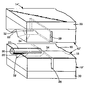
FIG. 4 shows one end of one embodiment of housing 40 having
substrate 42 and covering 44, both of which are reinforced with backings 46.
In sub~ e 42, waveguide ch~nnel 48 is sep~ tç~1 from fiber-~ nm~nt groove
25 50 by gap 52. In covering 44 are fiber-~ nment groove 50 and gap 52.
Fiber-~lignmPnt grooves 50 narrow (horizontally) and taper (vertically) from
opening 54.
FIG. 5 shows one end of one embodiment of mold 60 having waveguide
çh~nnPl rib 62 and ~lber-~lignment groove ridge 64 sep~r~t~d by gap-forming
30 piece 66. Fiber-~lignment groove ridge 64 narrows and tapers from edge 68
toward gap-forming piece 66. (The mold for a covering has been omitted for
the sake of clarity.)
Wo 95/01580 PcT/uss4/06096
FIG. 6 shows one end of one embodiment of master 70 having substrate
member 72 and covering member 74. Both members comprise waveguide
ch~nnelc 76 and fiber~ nmPnt grooves 78 sep~r~tPA by gaps 80. The portions
of substrate member 72 and covering member 74 in which waveguide ch~nnPl~
76 are inscribed are covered by a thin layer of photo-resist m~teri~l 82. Fiber-
~lignmPnt grooves 78 narrow and taper from opening 84.
DETAILED DESCRIPTION OF PREFERRED EMBODIMENTS
Preparation of the optical coupler of the present invention requires the
10 formation of a master. Prom this master are made d~llght~Pr molds on which
are microreplicated optical couplers of the present invention. An optical
coupler of the present invention is made directly from a d~llghtçr mold which,
in turn, is made by electroplating on a master. Therefore, the master will
nece5~,ily have the same pattern as the desired coupler, and a mold made from
this master will have a complem~nt~ry (reverse) pattern, i.e., the mold must
have raised ribs where grooves are desired on the optical coupler.
Once a master with the desired waveguide ch~nnel pattern is formed,
providing multiple ~llghter molds is relatively easy and inexpensive. Once
these molds are made, they can be used to mass produce the optical coupler of
20 the present invention. This is in stark contrast to the present manner of
producing optical couplers which involves the labor intensive step of fusing
optical fibers to one another or ~tt~rhing them to a planar, glass integr~trd
optical device.
I. M~king the Master
Rec~nse the rl~llghtçr molds will have ~limPn~ nal tolerances which are
complem~nt~ry to those of the master from which they are formed, great care
must be taken in forming the masters. Particularly, the waveguide ch~nnçl~ and
fiber grooves must be dçlinP~ted in the master to precise toler~nres. More
particularly, where (for example) single mode operation is desired, ch~nntol~
3 0 with an 8 x 8 ~m2 cross section must be aligned to submicron precision with
fiber grooves which hold fibers having a much larger c~ ding radius (e.g.,
WO 95/01580 ?16~1 o ~ PCTtUS94/06096
62.5 ~m). Additionally, the vertical walls of those channels must be quite
smooth to reduce light scattering loss.
In choosing m~tPri~l~ from which to make the master, the primary
l~ui~ ent is that the m~t~r~ be capable of being patterned with (a)
5 ch~nn~l.c, ranging in width and depth from approximately 8 ~m to
a~r~xim~tPly 100 ~m, the walls of which are smooth to a submicron scale,
and (b) grooves which can hold optical fibers. A variety of m~tPri~l~ incl~1~ingpolymer films, silicon oxide, and silicon nitride can be used to form the master,
depenrling on the method chosen to form the ch~nnel~ and grooves. Re~ e
10 photolithography combined with wet development in photo-resist has proven to
be a ~ felled method of ch~nnPl formation and photolithography in silicon
using anisotropic etching has proven to be a ~ felled method of groove
forma~ion, a particularly ~ felled m~teri~l is silicon coated with a photo-resist
m~t,Pri~l .
Rec~ P the housing which will eventually be formed from the master
will comprise two members, i.e., a substrate and a cover, the master must
comprise the exact d~-pli~tPs of thèse mpmb~rs Preferred methods of forming
these mPmhers are tli.~cu~sed below.
A. Sul~sl~ale
Potential methods for forming grooves and çh~nnPl.s include diamond
turning, laser ablation, and photolithographic techniques. The usefulness of thefirst of these techniques is severely limited by the difficulty involved in forming
curved ch~nnPl~ and grooves with abrupt ends. Rec~use the present invention
involves the formation of passive optical couplers in which curved ch~nnel.c
25 may be np~æe~y (because light from a single fiber may be split into a number
of output fibers), and because fiber ~lignmPnt grooves may end abruptly at the
beginning of waveguide ch~nnPl~ the applicability of diamond turning as a
groove- and ch~nnel-forming method is quite limitPA
Although laser ablation offers the nPces~ry flexibility in the generation
~ , ,
3 o of waveguide ch~nnel pZ~tt,Prn~:, it is not as routinely used in the micro-
electronics industry and is thus not as fully developed as photolithography.
Preferably, photolithographic techniques are used to form the nece~ry
- grooves and ch~nnP1~ of the present invention. More spe~ifi~lly, ch~nmPl~ can
_g_
Wo 9~/01580 ~ 08 PCT/US94/06096
be formed in photo-resist by common mask and exposure development
techniques. Fiber-holding grooves can be formed in Si crystal wafers by
photolithographic patterning followed by anisotropic etching in a basic solution,
e.g., a KOH solution. The procedures used to form these grooves and channels
5 are discussed more fully below.
1. Grooves
Recall~e silicon has been found to be particularly ~mPn~hle to the
following etching process and is therefore a prefe red material, it has been used
for the ~ oses of the following discussion. Silicon crystal (100) wafers are a
0 particularly ~c;rel~d base m~tPri~l for the master substrate. However, those
skilled in the art will recognize that the following method can be adapted for
use with a variety of base m~tt-ri~l~
In order that input and output optical fibers be securely held in and be
precisely aligned with the channel waveguides of the housing which will result
15 from the master, grooves capable of holding such fibers must be formed in theend portions of the silicon crystal wafer. Using a simple l x 2 splitter as an
~y~mple, one end of the wafer will have a single groove whereas the other will
have two grooves. The plc;felled method for forming these grooves is well
known and can be found in a number of sources including Tsang et al., Applied
20 Optics, 14, 1200 (1975).
On a clean silicon wafer is deposited a m~king layer such as silicon
nitride, or silicon oxide. This layer can range in thickness from 50 to 200 nm,
although 100 nm has been found to work particularly well. This layer is then
p~tterned by means of conventional photolithography. For instance, a photo-
25 resist m~t~ri~l can be spin coated onto the surface of the substrate, preferablyafter the application of an adhesion promoter. After heating to remove solvent
(i.e., soft baking), the fiber groove pattern is applied by exposing the photo-
resist to a light source, preferably a source of ultraviolet light such as a
mercury lamp, through a mask aligned in the < 110 > crystal direction. Once
3 o p~tt~rnerl~ the photo-resist is developed according to processes well known in
the art.
The p~tt~rn~A, exposed silicon nitride m~ing layer is then etched by
one of a number of well known means in the art, although reactive ion etching
--10--
~ = ~
Wo 95/01580 ~ PCTtUS94t06096
(e.g., CF4 and oxygen) has been found to be a plcrelled etching means. By
carefully controlling the etching time and rate, the desired amount of the
patterned m~king layer is etched to expose the substrate m~t~ri~l (e.g., siliconwafer). Once this is completed, rem~ining photo-resist is removed by rinsing
s with an organic solvent in which the photo-resist is soluble. A common solventfor this ~L~ul~ose is an ~cetoll~/iso~ropanol solution. I~mn~nt~ of photo-resistcan be removed by rinsing in an acidic medium.
Once the m~king layer has been etched, the silicon crystal wafer is
anisotropically etched with a strongly basic solution. A particularly pl~fe,led
10 etching solution is an aqueous 30% (by weight) potassium hydroxide solution.
This step can be ~;,rornled at an elevated le"~pel~ture to decrease the amount
of time necç~ry to complete the groove-formation etching. A temperature of
80C has been found to provide a suf~lciently short etching time.
F.tching depth can be controlled by adjusting the concentr~tion of the
15 etching solution, the lenl~eldturt; at which the etching is carried out, the amount
of time the etching solution is allowed to contact the substrate, or a combination
of these factors. Controlling groove depth is illlpolL~l to ensure optimum
nm~ t of the optical fibers to the waveguide ch~nnel~. Using a single mode
fiber as an example, a groove width (at the upper surface of the substrat* in
the range of 140 to 160 ,um is desirable to ensure that the core of the insertedfiber (approxim~t~ly 62.5 ,um from the surface of the fiber) is at the same
height as the collc~onding channel waveguide core. (This groove width is
somewhat greater than might appear optimal to account for iimçn~ional changes
inherent in the polymeric housing forming process ~ cl-~se~i below.) Groove
2s depths can range from about 50 to 500 ~m, preferably from 60 to 200 ~m,
depending on the type of fiber which is to be used. Grooves should be of such
a length that fibers inserted in the grooves of the result~nt housing will be
securely held and supported. Groove lengths as small as 1 mm could be
effective for this pul~ose, although lengths of about 3 mm are ~rer~ d.
For some applications, providing a tapered groove may be desired (i.e.,
to aid in the insertion of fibers). For in~t~nce, a groove which (horizontally)
narrows ~rom the outside edge toward the waveguide c~l~nn~l and which
--11--
~ 1 6 ~
Wo 95/01580 . PCT/US94/06096
(vertically) tapers in the same direction might make easier the fiber insertion
process.
Once the desired grooves are etched, the rem~ind~r of the silicon nitride
m~king layer is removed. This is accomplished by the same type of m~king
5 layer etching as described above.
When completed, this process provides a silicon crystal wafer with the
desired groove pattern etched therein.
2. Ch~nn~l~
On the center portion of the patterned silicon crystal wafer, i.e., that
10 portion between the two sets of grooves, is deposited another photo-resist layer,
preferably after the application of an adhesion promoter. This layer can be
applied to a thicknçc~ of up to 200 ~m, preferably up to 100 ,~m. This photo-
resist layer is then p~ttern~l, ir.~ t~d, and developed as described in the
groove formation process.
Con~rolling the ~limen~ions of the ch~nnPl~ is of great import since the
ch~nnel ~lim~n~ions should be as close as possible to the ~limen~ions of the core
of an optical fiber. Channel widths and depths are carefully controlled by
precisely decigning the mask pattern, moniluling the time the photo-resist is
exposed to a light source (as described above), adjusting the amount of time the2 0 developer is allowed to etch the photo-resist, or a combination of these
variables. Widths and depths range from 1 to 200 ,um, preferably from 5 to
100 ~Lm, even more preferably from about S to 8 ~m, and will depend on the
type of fibers which are to be aligned with these ch~nn~l~. For in~t~nce, where
single mode optical fibers ope ~ting at 1.31 and 1.55 ~m wavelengths are to be
25 coupled, çh~nnPl widths and depths will be approximately 8 ,um, the ~ mçt~.r
of a single-mode fiber core.
In some applications, the groove-forming process may leave a beveled
portion of silicon crystal wafer between the ch~nn~ls and the bottom of the
grooves. This can be collæled by cutting across the groove/channel interface
30 so as to form a trench between the fiber-holding groove and the waveguide
ch~nn~l. A diamond-edged saw can be used to effect this cut.
The spin coating process (used in applying the photo-resist m~tçri~l)
tends to produce an accumulation of photo-resist m~t~.ri~l at surface
o ~
WO 95/01580 . PCT/US94/06096
discontim-itiPs (i.e., groov~s~ t~umulations hinder the formation of
çh~nnelc of uniform depth. To reduce these accumu-lations, a succescion of
photo-resist applications by high-rpm spin co~tingc and dryings can be used to
build a layer of proper thicknPss This method provides better control of
5 photo-resist thickness uniformity than does covering the wafer with photo-resist
m~tPri~l and subjecting it to a single low-rpm spin coating process. Once
photo-resist has been deposited, photo-resist m~t~ri~l at the groove/channel
interfaces is photolithographically removed up to 1 mm, preferably a few
hundred microns, from the edge of the groove/ch~nnel interface. In other
10 words, the ch~nnPl mask is decignPcl so that, between the ch~nnelc and the
grooves, is a perpindicular gap up to 1 mm wide. When the photo-resist is
exposed and developed, this perpindicular gap creates a small space between the
ends of the ch~nnPl.c and the ends of the grooves. The portions of the substrateexposed by the formation of these spaces can be cut with a diamond-edged saw,
15 preferably at the same time the beveled portion of the silicon crystal wafer is
being cut, to at least the same depth as that of the lowest point of-a fiber
inserted into a substrate groove so that such a fiber has a clear path to the edge
of the corresponding waveguiding ch~nnel
If desired, reservoirs can be cimil~rly etched or cut into the portion of
20 the sulJsL~ e in which the waveguiding ch~nnPlc are located. These reservoirsact as means of capLu~ g and storing any excess monomer used to fill the
rh~nn~lc of the housings produced from these masters. These reservoirs are
app~ im~t~ly the same length as the ch~nnelc (i.e., at least a few millime-ters),
but their widths and depths will be lar~er so as to ensure that a substantial
25 portion of any excess monomer is caplùr~d. They are connected to the ends of
the ch~nnPlc by means of a trench which perpendicularly connects the ch~nnelc
and reservoirs. This trench preferably is cut in the gap ~i~cllsced in the
prece~ling paragraph.
B. Covering
This member is formed in much the same way as the substrate. In other
words, grooves and ch~nnPlc are formed in the silicon substrate as described
above. If ch~nn~lc are also formed in the covering, the depth of the ch~nnPl in
the substrate should be adjusted so that the depth of the whole ch~nnPI is the
--13--
WO 95/01580 ~ 8 PCT/US94/06096
same as the ~ metPr of the fiber core. However, the channel-formation step
can be elimin~ted so that a flat covering is obtained. Doing so elimin~tes the
possibility that the covering ch~nnel(s) will be improperly aligned with the
substrate ch~nnel(s) once the housing pieces are formed.
~ltern~tively, ch~nnP-lc can be formed in the covering only. This can
result in the ~olimin~tion of the ch~nnel-formation step described above for thesubstrate. This alternative results in masters from which will be formed
housing substrates which are flat, i.e., all light tr~n~mitted by the housing will
be through the ch~nn~l waveguide core located completely in the covering.
10 II. ~king the Mold
Molds are made from the masters of the previous section by an
electroplating process. This produces a durable metal mold with the desired
groove and ch~nnel p~tt~rn~.
A silicon/photo-resist master is first coated with a film of a metal such
15 as nickel, copper, zinc, silver, or an alloy of a metal, to provide a conductive
seed layer. This seed layer is preferably about 20 nm thick. The coated master
is electroplated with about 0.64 mm (25 mils) of a metal such as nickel,
copper, zinc, or silver, although nickel is particularly ~lefcll~d. A particular-
ly plcrcllcd mold is nickel electroplated on a nickel seed layer.
The mold is then SeP~IA~ from the master. This can be done by any
physical means such as prying apart the two pieces. Release of the master from
the nickel mold can be enh~nced by first depositing a silicon oxide coating on
the silicon/photo-resist surface (of the master) using plasma enh~nced ch~mic~l
vapor deposition. This release layer preferably has a thickne~ of about
100 nm.
m. Microreplication of the Housing
A housing of the present invention comprises a substrate and a covering.
The~cforc, both members must be formed on their respective molds. Both
substrates and coverings can be formed by either casting or injection molciing
3 0 techniques.
When assembled, the optical couplers of the present invention are up to
a few centimeters in length and have a thicknec~ of up to a few millimetPr~,
Wo 95/01~0 2 ~ 6 ~ PCT/US94/06096
although couplers which are as small as possible are normally desired. The
width of the coupler will be depend on the number of input or output fibers
which are to be inserted. For instance, simple 1 x 1 or 1 x 2 couplers can be
made quite narrow (i.e., approximately the width of two optical fibers) whereas
5 couplers with 20 or more input or output fibers would be significantly wider.
The housing substrate and covering should have an index of refraction
which is quite similar to, preferably within 1 x 10⁴, that of the optical fiber
c1 lding. Although few compounds have such a refractive index, mixtures of
monomers (or monomer precursors) with higher and lower refractive indices
10 can be combined to provide a monomer Illi~Ul`t; which, upon polymPri7~tion,
has the desired index of refraction. Polymers useful in forming the housings of
the present invention include epoxies, poly(meth)acrylates, poly(vinyl
a_lactones), poly(urethanes), and poly(ureas). These polymers can optionally
be substituted with atoms such as fluorine and deuterium in order to reduce
15 their r~fractive indices and to reduce absorptive losses in nea~ infrared
wavelengths. Additionally, colloidal silica, such as that described in U.S.
Patent No. 4,885,332, can be added to the monomer Illi~Lw~ from which the
above polymers are formed to provide lower refractive indices and reduced
therm~l expansion coeffici~ont~.
An example of a suitable monomeric combination is PhotomerTM 4127
propoxylated neopentyl glycol diacrylate (Henkel Corp.; Morristown, NJ) or
ethylene glycol riimeth~crylate (Aldrich Chem. Co.; Milwaukee, WI) mixed in
a ratio such as 89:11 (by weight) with perfluoro-cyclohexyl acrylate (Pc~A), as
described in U.S. Patent No. 4,968,116 (col. 11), with a~lu~imately 1% (by
weight) of a photoinitiator such as IrgacureTM 651 2,2- (1im~thoxy-2-
phenylacetophenone (Aldrich). Cros~linking agents, e.g., multifunctional
aclylates such as trimethylol propane triacrylate ~TMPTA) (Scientific Polymer
Productss Inc.; Ontario, NY), can also be added to reduce solubility and to
raise the glass transition ten~el~ture of the polymer.
No matter which of the following techniques is chosen, the reslllting
substrate member of the housing will comprise grooves for holding input optical
fibers on one end, grooves for holding output optical fibers at the other end,
and the desired ch~nn~l pattern between the two sets of grooves. Recall~e of
--15--
0 8 ~
WO 9~/0l580 . PCT/US94/06096
the precise etching of the master (described above), fibers which are inserted
into the grooves will be aligned with the corresponding ch~nnel entry or exit.
A. Casting
The casting technique basically involves the steps of pouring a liquid
5 monomer or a mi~lul~ of monomers onto a mold and then curing it/them.
Enough monomer or monomer mixture should be used to at least fill the
grooves and cover the face of the mold, inçlndin~ the grooves and waveguide
~h~nn~
If desired, a release agent such as Mold Release 225 (RAM Products;
10 Gardenia, CA) can be applied to the mold prior to application of the
monomer(s) to f~ilit~t~ sep~r~tit)n of the housing from the mold.
Once the monomer (or ~ re of monomers) has been poured on the
mold, a stiff b~cking such as a sheet of poly(methylm-oth~crylate),
poly(carbonate), or a metal such as ~ minum or st~inlec~ steel can be pressed
15 against the monomer. This may be desired where the substrate must display a
certain amount of structural integrity.
The monomer (or monomer plus b~cking combination) is then cured by
any of a variety of photo or thermal means known in the art. The cured
housing, plus b~ ing if one was used, is then physically sep~lilted from the
2 o mold.
If a polymeric b~t king has been used, the b~cl~ing can be oxygen plasma
treated to enhance its adhesion to the polymeric housing. This involves placing
the backing in a reactive ion etching chamber, having an oxygen atmosphere
(approxim~tely 26.7 Pa, i.e., 200 millitorr), for approximately ten min~tes. If
25 a mPt~llic b~king has been used, its adhesion to the substrate can be promoted
with an ~-lh~ion enh~ncer.
B. Injection Mol-ling
Standard molding techniques known in the art may also be used to form
the housings of the present invention. These techniques require that molds be
3 o placed in an injection mol~ling apparatus where polymers with suitable optical
pr~ellies (such as those described in the "Casting" section) be injected and
then se~ tçd from the mold.
--16--
~ 2~ 8 ~ ~
Wo 95/01~80 . PCTIUS94/06096
A b~cking can be glued onto the replicated housing prior to or after the
housing is separated from the mold.
IV. ~semhlinE the Coupler
Once a housing with the desired pattern has been l,l~al~d, a few simple
5 steps will produce a passive optical coupler where the input and output optical
fibers are precisely aligned with the corresponding ch~nnel waveguide cores.
A mixture of one or more polymeri7~hle monomers is poured into the
ch~nn~l.c ~ormed in either or both of the substrate and covering members.
Monomers similar to those used in making the substrate and covering, inclufling
10 fluorinated and deule,~ted derivatives as well as colloidal silica-cont~ining monomers, can be used. Once the monomer (or mixture of monomers) has
been cured so as to produce waveguiding cores, the refractive indices of those
waveguiding cores is preferably as close as possible to the refractive indices of
the cores of the optical fibers to be inserted. Additionally, for single mode
15 fiber waveguides, the index of refraction of the waveguiding core polymer (i.e.,
the cured monomer) preferably is no more than 7 x 1o-3 greater than and no
less than 2 x 10⁻³ the refractive index of the housing. (Where mllltimode
fibers are to be used, this dirrel~;nce between the indices of refraction of thewaveguiding core polymer and the housing is preferably no more than 0.5.) If
20 desired, multifunctional acrylates and meth~crylates, such as TMPTA, can be
added to the composition to crosslink the waveguiding core polymer.
Cleaved or polished optical fibers are then inserted into the grooves of
the piece in which the ch~nn~ are located. af ch~nn~l.c have been formed in
both pieces, the fibers can be inserted in the grooves of either piece.) The
25 other housing member is then placed on the first so that its grooves and those
of the first piece form a snug fit around the optical fibers. The assembly may
then be cured when desired by any of a variety of photo or thermal means
known in the art. The fibers will preferably be butted directly against the
ch~nnPl waveguide core, although a slight amount of separation between the
30 fiber and the ch~nnpl waveguide core does not ~ignific~ntly affect coupling
efficiency.
2 ~
wo 95/01~80 - . PCT/US94/06096
Alternatively, the covering and the substrate can be filled with liquid
monomer(s) after inserting the optical fiber. Once the pieces are fit together to
form the housing assembly, the monomer(s) can be cured as described
imm~i~t~ly above.
To make easier the ~ligning of the grooves and ch~nn~ of the substrate
and covering, the pieces can be adapted to include conventional f~t~ning
means. For instance, the substrate master can be modified to include one or
more small protuberances, while the covering master can be modified to include
complem~nt~ry small recesses which fit over the protuber~n~es. Alterna-tively,
0 the covering could include the protuberances while the substrate cont~ined the complementary recesses. One of the pieces might also be formed with an
encircling ridge which slide fits into a complementary encircling trough in the
other piece.
Once the coupler has been assembled, it can be placed in a protective
15 jacket. This jacket can be either polymeric or m~t~llic.
Objects and advantages of this invention are further illustrated by the
following examples. The particular m~t~ri~ and amounts thereof, as well as
other conditions and details, recited in these examples should not be construed
to unduly limit this invention.
EXAMPLES
Example 1: Formation of Grooves in Master
On a clean, three-inch silicon wafer was grown a layer of silicon nitride
25 (approximately 100 nm) using a mixture of 60 standard cubic c~ntim~t~rs per
minute (sccm) NH3 and 20 sccm dichlorosilane at 800C for about thirty
".i~ les.
To this silicon nitride layer was spin coated an excess of Shipley C-50~
adhesion promoter (Shipley Co., Inc.; Newton, MA) which was then dried for
30 a few ~ es at room te,-,pt;l~ture. Thereafter, an excess of Shipley 1818
photo-resist was spin coated on the silicon nitride layer at 4000 rpm.
The coated wafer was then baked at 90C for approximately thirty
s. After the wafer was removed from the heat source, a mask with a 1-
--18--
wo 95/015~ 8 PCT/US94/06096
input fiber/1-output fiber pattern was aligned along the < 110 > crystal
direction. The photo-resist was patterned by exposing the masked wafer to a
mercury lamp (A = 400 nm) at 5.5 mW/cm2 for about 20 seconds. The mask
was removed, and the photo-resist immersed with Shipley 319 developer. The
5 wafer was then washed with water and thoroughly dried (approximately five
mimltes) at 120C.
The silicon nitride in the area of the fiber grooves was removed by
reactive ion etching (20 sccm of CF4 and 0.5 sccm of oxygen for approximately
five minutes). ~2~ inillg photo-resist was removed by rinsing the master in an
10 acetone/isopr~allol solution, then in an H2SO4/H2O2 solution.
The exposed areas of the silicon wafer were then etched with an aqueous
solution of 30% (by weight) KOH at a le~ ture of 80C and a rate of 1.4
~m/min. Rec~-se the wafer had been patterned along the < 110 > crystal
direction, V-shaped grooves were formed. These groove were 125 ,um deep
15 and 3 mm long.
The silicon nitride which rem~ined between the grooves was removed by
reactive ion etching in 20 sccm of CF4 and 0.5 sccm oxygen for a~loximately
~lve ",i~ s~
2 0 Example 2: Formation of Ch~nn~ in Master
The V-grooved silicon wafer from Example 1 was coated as in Exàmple
1 with Shipley C-50~ adhesion promoter. Thereafter, an excess of Shipley
STR1075~ photo-resist was spin coated onto the wafer at 3800 rpm for about 60
25 seconds. The wafer was then dried at 100C for a~ru~imately two min~1tes.
The res~ in~ photo-resist layer had a thickness of 7.5 ,um.
A mask with a 1 x 1 pattern was then placed on the coated substrate.
The llnm~ d areas of photo-resist were then exposed to a mercury lamp (~ =
400 nm) at 5.5 mW/cm2 for about 80 secon~l~. The mask is then removed, and
30 the photo-resist washed with Shipley 319 developer for about 60 seconds. The
coated wafer was then rinsed with water and dried.
--19--
~ ~ 4~
Wo 9~/01~80 . PCT/US94/06C96
The beveled ends of the V-shaped fiber-~ nmPnt grooves were
removed by dicing a 75 ~m-wide trench across the ends of the grooves at the
groove - rh~nnel interface with a diamond-edged saw.
.
Example 3: Making the Mold
On the grooved and ch~nneled silicon/photo-resist master from Example
2 was deposited a 100 nm layer of silicon oxide to act as a release layer. This
was done by plasma-e-nh~nçed chemical vapor deposition, at room tem~el~lulc;,
10 with 40 sccm N2O and 8 sccm SiH4. On this release coating layer was
deposited, by electron beam evaporation, an approximately 20 nm seed layer of
nickel.
The nickel-coated master was then mounted onto a sPinless steel plate,
and this assembly was immersed in a 50C nickel sl-lf~m~te solution cont~ining
15 a nickel counterelectrode. A current density of 0.022 A/cm2 (20 A/ft2) was
applied so as to plate 25.4 ~m (1 mil) of nickel per hour.
After a 0.51 mm (20 mil) coating had been applied, the assembly was
removed and rinsed with water. The nickel mold was then carefully pried away
from the silicon/photo-resist master.
Example 4: Backing for Housing
Two 0.56 mm (22 mil) thick sheets of poly(methyl-meth~crylate)
(PMMA) were treated with oxygen plasma (26.7 Pa at room tempel~ure) for
25 ap~ro~i",alely 10 minutes in order to improve adhesion between them and the
polymeric housing m~t~ l These treated PMMA sheets were cut to 3.5 cm
x 6cm.
Example 5: Cast-and-cure Microreplication of Housing
The nickel mold from Example 3 was treated with Mold Release 225D
(RAM Products) to f~cilit~te release of polymer from the mold.
Thel~fLer, an 89:11 (byweight) ~ lureofPhotomer4127~(Henkel)
pro~ylated neopentyl glycol diacrylate and perfluorocyclohexyl acrylate
35 monomers with 0.5% (by weight) of Darocure 1173 photoinitiator (Ciba Geigy
--20--
=
WO 95/01~80 ~1 4~1 ~8 PCT/US94/06096
Corp.; Ardsley, NY) was poured onto the nickel mold. The backing m~t~ri~l
from Example 4 was pressed against the monomer mixture, with the oxygen-
treated surface facing the monomers.
The mold/backing assembly was exposed to a mercury lamp (200 watts
5 of electrical power over an area of 100 cm2) for about 10 minutes. Once
exposure was complete, the housing/backing unit was pried away from the
nickel mold. A diamond-edged saw was used to cut the housing/
b~-king unit into a 1 cm x 4 cm rectangle.
Example 6: Assembling the Coupler
A polymeric substrate with one fiber-~ligning groove at each end and a
straight çh~nn~l connection between the two grooves was placed on a metallic
block with numerous holes drilled therein. By applying vacuum suction to the
15 bottom of this block, the substrate was held tightly to thereto.
SMF-28 optical fibers (Corning Inc.; Corning, NY), which propagate a
single mode at ~ = 1.3 ,um, were ~re~ed for insertion by cleaving. This
provided a subst~nti~lly flat end face. One of these cleaved fibers was placed
into one of the fiber-~ ning grooves of the substrate and held in place by a
20 spring-loaded clip located a few millimPter~ from the edge of the substrate.
The other fiber was ~imil~rly inserted and held.
A ",ix~ure of monomers and photoiniti~tor similar to that described in
Example 5 [with 7% (by wt.) PcHA] was pl~pared. One drop of this was
placed on the substrate and inserted fi~ers. This drop was s~lfficient to coat the
2s substrate and to fill the ch~nnPI and grooves.
A ;polymeric covering with fiber-~ligning grooves in resgistry to those of
the substrate was placed (groove side down) on the monomer-coated substrate.
A glass slide was placed on top of the covering and pressed downward to
squeeze out excess monomer and to fit the covering tightly around the fibers.
The glass slide was then secured with a pres~ure sensitive adhesive tape
to the metal block. The secured coupler was exposed to a mercury lamp (same
conditions as in Example 5) until the monomer ~ixLule had cured. The PSA
--21--
WO 95/01580 ~ ~ 6~ ~ ~ 8 PCT/US94/06096
tape and the glass slide were removed from the coupler, and the coupler was
removed from the metal block.
~xample 7: Optical Coupling Efficiency
In a re~ ted straight çh~nn~l polymeric substrate attached to a metal
block (see Example 6) were inserted two fibers plepaled as described in
FY~mrle 6. The ch~nnel width of this substrate was 9 ~m, and the width at the
top of the V-shaped grooves was 157.5 ~m. A drop of index-m~tching oil with
10 nD = 1.56 (R.P. Cargill Laboratories, Inc.; Cedar Grove, NJ) was placed on
the substrate to act as a waveguiding m~ m.
A covering with colre~ollding fiber-~ligning grooves was temporarily
~ffixed, groove side up, on a tr~n~p~rent glass block by means of a drop of
water. The covering/
15 glass block combination was then inserted into a recessed hole in a metal plate,
and the glass block was cl~mped to the metal plate. The covering/blocWplate
was inverted, placed above the ~ubslldte, and çl~mre~l so that the grooves in the
cover were subst~nti~lly aligned with those in the substrate.
The metal block to which the substrate was ~tt~h~d was then laterally
20 positinnpd so as to optimiæ the ~lipnment of the fiber grooves. After
nm~nt was optimi~ed (as viewed lhrougll a microscope), the metal
block/subslldle piece was tr~n~l~ted upward until the substrate was co~ )ressed
against the covering.
Light at a wavelength of 1.31 ~m was l~lln~hecl into the end of one
25 optical fiber. Measurement at the end of the fiber (prior to insertion into the
s~.At.o,) showed 1.68 mW at the ~nt~nce to the waveguide ch~nnPl. Output
power was measured at the end of the opposile optical fiber. This number was
ratioed against the input power to give a total insertion loss of 9.7 dB.
Although coupling con-1itions in this eY~mple were not optimi7ed, some
3 0 output power was observed. This shows that the couplers of the present
invention can passively align input and output optic~ fibers.
--22--
WO 95/01580 2~ $ PCT/US94/06096
Various mo~ific~ti~ n and alterations which do not depart from the scope
and spirit of this invention will become apparent to those skilled in the art.
This invention is not to be unduly limited to the illustrative embo~imçnt~ set
forth herein.
!
--2 3--
`.