Note : Les descriptions sont présentées dans la langue officielle dans laquelle elles ont été soumises.
WO 95/00202 ~ ~ ~ ~ PCT/US94/05179
1
This invention relates to the field of implantable medical devices, and
more particularly relates to implantable medical device systems which include
a
telemetry subsystem.
Since the introduction of the first implantable pacemakers in the
1960's, there have been considerable advancements both in the field of
electrondcs and the field of medicine, such that there is presently a wide
assortment of commercially-available implantable medical devices. The class of
implantable medical devices now includes not only pacemakers, but also
implantable cardioverters, defibrillators, neural stimulators, and drug
administering devices. Today's state-of the-art implantable medical devices
are
vastly mmore sophisticated and complex than early pacemakers, capable of
performing significantly more complex tasks. The therapeutic benefits of such
devices have been well-proven.
As the functional sophistication and complexity of implantable medical
devices has increased over the years, it has become increasingly more
important
for such devices to be equipped with a telemetry system for enabling them to
communicate with an external unit.
For example, shortly after the introduction of the earliest fixed-rate, non-
inhibited pacemakers, it became apparent that it would be desirable for a
physician to non-invasively exercise at least some amount of control over the
device, e.g., to turn the device on or off or adjust the fixed pacing rate,
after
implant. In early devices, one way the the physician was able to have some
control .over implantable device operation was through the provision of a
magnetic reed switch in the implantable device. After implant, the reed switch
would be actuated by placing a magnet over the implant site. Reed switch
closure could then be used, for example, to alternately activate or deactivate
the
device. Alternatively, the fixed pacing rate of the device could be adjusted
up or
down by incremental amounts based upon the duration of reed switch closure.
Many dnfferent schemes utilizing a reed switch to adjust parameters of
implanted
66742-539
CA 02164963 2000-08-21
2
medical devices have been developed. See, for example, U.S.
Patent No. 3,311,111 to Bowers, U.S. Patent No. 3,518,997 to
Sessions, U.S. Patent No. 3,623,486 to Berkovits, U.S. Patent
No. 3,631,860 to Lopin, U.S. Patent No. 3,738,369 to Adams et
al., U.S. Patent No. 3,805,796 to Terry, Jr., and U.S. Patent
No. 4,066,086 to Alferness et al.
As new, more advanced features are incorporated into
implantable devices, it is typically necessary to convey
correspondingly more information to the device relating to the
selection and control of those features. For example, if a
pacemaker is selectively operable in various pacing modes
(e.g., VVI, VDD, DDD, etc...), it is desirable that the
physician or clinician be able to non-invasively select a mode
of operation. Similarly, if the pacemaker is capable of pacing
at various rates, or of delivering stimulating pulses of
varying energy levels, it is desirable that the physician or
clinician be able to select, on a patient-by-patient basis,
appropriate values for such variable operational parameters.
Even greater demands are placed upon the telemetry
system in implantable devices having such advanced features as
rate adaptation based upon activity sensing, as disclosed, for
example, in U.S. Patent No. 5,052,388 to Sivula et al. entitled
"Method and Apparatus for Implementing Activity Sensing in a
Pulse Generator" and in U.S. Patent No. 5,312,453, issued on
May 17, 1994 to Shelton et al., entitled "Work-Modulated Pacing
Rate Deceleration".
The information which must be communicated to the
implantable device in today's state-of-the-art pacemakers
includes: acing mode, multiple rate response settings,
electrode polarity, maximum and minimum pacing rates, output
66742-539
CA 02164963 2000-08-21
2a
energy (output pulse width and/or output current), sense
amplifier sensitivity, refractory periods, calibration
information, rate response attack (acceleration) and decay
(deceleration), onset detection criteria, and perhaps many
other parameter settings.
WO 95/00202 PCT/US94/05179
~~6~~s~
3
'lChe need to be able to communicate more and more information to
implanted devices quickly rendered the simple reed-switch closure arrangement
insufficient. Also, it has become apparent that it would also be desirable not
only to allow information to be communicated to the implanted device, but also
to enable the implanted device to communicate information to the outside
world.
For diagnostic purposes, for example, it is desirable for the implanted
device to be able to communicate information regarding its operational status
to
the physician or clinician. State of the art implantable devices are available
which G~an even transmit a digitized ECG signal for display, storage, and/or
analysis by an external device.
As used herein, the terms "uplink" and "uplink telemetry" will be used to
denote the communications channel for conveying information from the
implanted device to an external unit of some sort. Conversely, the terms
"downlink" and "downlink telemetry" will be used to denote the communications
channel for conveying information from an external unit to the implanted
device.
i,7arious telemetry systems for providing the necessary communications
channels between an external unit and an implanted device have been shown in
the art. Telemetry systems are disclosed, for example, in the following U.S.
Patentso U.S. Patent No. 4,539,992 to Calfee et al. entitled "Method and
Apparatus for Communicating With Implanted Body Function Stimulator' ; U.S.
Patent No. 4,550,732 to Batty Jr. et al. entitled "System and Process for
Enabling
a Predefined Function Within An Implanted Device"; U.S. Patent No. 4,571,589
to Slocum et al. entitled "Biomedical Implant With High Speed, Low Power Two-
Way Telemetry' ; U.S. Patent No. 4,676,248 to Berntson entitled "Circuit for
Controlling a Receiver in an Implanted Device'; U.S. Patent No. 5,127,404 to
Wyborny et al. entitled 'Telemetry Format for Implanted Medical Device' ; U.S.
Patent No. 4,211,235 to Keller, Jr. et al. entitled "Programmer for Implanted
Device' ; U.S. Patent No. 4,374,382 to Markowitz entitled "Marker Channel
Telemetry System for a Medical Device' ; and U.S. Patent No. 4,556,063 to
Thompson et al. entitled "Telemetry System for a Medical Device".
Typically, telemetry systems such as those described in the above-
referenced patents are employed in conjunction with an external
programming/processing unit. One programmer for non-invasively programming
66742-539
CA 02164963 2000-08-21
4
a cardiac pacemaker is described in its various aspects in the
following U.S. Patents to Hartlaub et al., each commonly
assigned to the assignee of the present invention: U.S. Patent
No. 4,250,884 entitled "Apparatus For and Method Of Programming
the Minimum Energy Threshold for Pacing Pulses to be Applied to
a Patient's Heart"; U.S. Patent No. 4,273,132 entitled "Digital
Cardiac Pacemaker with Threshold Margin Check"; U.S. Patent No.
4,273,133 entitled "Programmable Digital Cardiac Pacemaker with
Means to Override Effects of Reed Switch Closure"; U.S. Patent
No. 4,233,985 entitled "Multi-Mode Programmable Digital Cardiac
Pacemaker"; and U.S. Patent No. 4,253,466 entitled "Temporary
and Permanent Programmable Digital Cardiac Pacemaker".
Aspects of the programmer that is the subject of the
foregoing Hartlaub et al. patents (hereinafter "the Hartlaub
programmer") are also described in U.S. Patent No. 4,208,008 to
Smith, entitled "Pacing Generator Programming Apparatus
Including Error Detection Means" and in U.S. Patent No.
4,236,524 to Powell et al., entitled "Program Testing
Apparatus" .
Although various different telemetry systems have
been employed in the prior art, the present inventors believe
that there remains a need for a telemetry system which is small
and consumes relatively little power, both being extremely
critical considerations in the context of battery-powered
implantable medical devices. Many of the known telemetry
systems (see, e.g., the above-referenced Calfee et al., Batty,
Jr. et al., and Slocum et al. patents) are implemented with
complex, energy-consuming circuits. Moreover, known telemetry
CA 02164963 2000-08-21
66742-539
4a
systems are often implemented in hardwired, non-flexible
circuitry not readily adaptable to more than one telemetry
protocol.
Additionally, the very existence of so many different
telemetry systems can itself be problematic, since even
different devices from the same manufacturer may employ
different and incompatible telemetry systems. From both a
marketing standpoint and a manufacturing standpoint, it is
costly and inefficient to require different programmers for
each different device made by a given manufacturer.
WO 95/00202 PCT/US94/05179
:2
1?or a given device, the uplink and downlink telemetry protocols may be
entirely different and incompatible, since considerations of energy
consumption
and efficiency are different for an implanted device than for an external
progranaming/control unit. From energy consumption and device cost
standpoints, the need for two different telemetry circuits in an implanted
device
is clearly undesirable.
The present invention, therefore, relates to a telemetry system particularly
well-suited for inclusion in a battery-powered implantable medical device.
In accordance with one aspect of the present invention, a telemetry system
is provided both for decoding downlink telemetry signals and encoding uplink
telemetry signals. The flexible circuit architecture in accordance with the
present
invention is small and consumes a relatively small amount of power. The
flexibility of the architecture enables the same telemetry circuit to be
utilized for
both uplink and downlink telemetry, and allows the circuit to be readily
adapted
for use with a variety of different telemetry protocols.
In accordance with an embodiment of the invention to be described
herein, an RF telemetry signal are received by an antenna in an implantable
medical device. The RF signal comprises a sequence of high-frequency pulses or
bursts. The disclosed embodiment uses pulse interval modulation to encode
downlink telemetry data, wherein the interval between trailing edges of RF
bursts
in the telemetry signal is modulated according to the digital data to be
transmitted to the implanted device. In particular, a shorter interval is
interpreted as a "0" bit, and a longer interval is interpreted as a "1" bit.
In
accordance with one feature of the present invention, however, it is believed
that
the telemetry system is readily adaptable to different types of telemetry
encoding
schemes, and may therefore be advantageously practiced in telemetry systems
not
employing pulse interval modulation.
In the telemetry system in accordance with the present invention, the
sequence of RF bursts in the downlink telemetry signal are converted to a
sequence of square wave pulses in a conventional manner. The square wave
pulses are then applied to a novel circuit which includes a programmable logic
CA 02164963 2000-08-21
66742-539
6
array (PLA) that is mask-programmable and which may also be
partially RAM programmable. The PLA serves as a central part
of the system.
For downlink telemetry, a counter is used to provide
a measure of various time intervals of interest (e. g.,
trailing-edge to trailing-edge intervals, pulse width
intervals, etc...) in the downlink telemetry signal. The
output from the counter is applied to the variable inputs of
the PLA. When a match between a counter value presented to the
PLA and a first programmed term of the PLA, a "0" bit is
shifted into a shift register in the telemetry circuit. When a
match between a counter value and another programmed term of
the PLA, a "1" is shifted into the shift register. Thus,
different downlink telemetry protocols may be supported by a
programmer incorporating a telemetry system in accordance with
the present invention, either by providing an appropriate PLA
for a given protocol, or by providing programming for multiple
protocols in a single PLA.
For uplink telemetry in one of the disclosed
embodiments, data is pulse-position encoded. The counter in
the telemetry system is used to define a plurality of time
slots in an uplink telemetry frame. The PLA in the telemetry
is programmed such that when a match between a counter value
and data to be transmitted occurs, an RF uplink telemetry pulse
is produced. In this way, a pulse is produced at a position
within the uplink telemetry frame which is proportional to the
data value to be transmitted.
The invention may be summarized, according to one
aspect as a telemetry system for communicating digital
information via a radio-frequency signal, comprising: an
antenna, adapted to receive said radio-frequency signal; an RF
CA 02164963 2000-08-21
66742-539
7
detect circuit, coupled to said antenna and responsive to said
radio-frequency signal to convert said radio-frequency signal
into a digital pulse stream; a clock, responsive to assertion
of a clock activation signal to produce a clock signal at a
clock output terminal thereof; a clock activation circuit,
coupled to said RF detect circuit to receive said digital pulse
stream, and coupled to said clock, said clock activation
circuit responsive to a first predetermined characteristic of
said digital pulse stream to assert said clock activation
signal, and responsive to a second predetermined characteristic
of said digital pulse stream to deassert said clock activation
signal; a counter, coupled to said clock output terminal and
adapted to present a plurality of count value output signals
representing said counter's count value at a plurality of
output terminals thereof, said counter responsive to a cycle of
said clock signal to increment said count value; a logic array,
coupled to said counter output terminals to receive said count
value output signals, and coupled to said RF detect circuit to
receive said digital pulse stream, said logic array responsive
to a first predetermined combination of said counter value
output signals and said digital pulse stream to assert a first
output signal indicative of a digital '~1" encoded into said
radio-frequency signal, said logic array responsive to a second
predetermined combination of said counter value output signals
and said digital pulse stream to assert a second output signal
indicative of a digital "0" encoded into said radio-frequency
signal.
According to another aspect, the invention provides a
telemetry system for receiving and decoding digital data
encoded in a radio-frequency signal, comprising: a telemetry
coil, adapted to receive said radio-frequency signal; a
detector circuit, coupled to said coil and responsive to a
CA 02164963 2000-08-21
66742-539
8
first predetermined characteristic in said received radio-
frequency signal to assert a wake-up signal and thereafter
responsive to a second predetermined characteristic in said
received radio-frequency signal to assert a detect signal; a
clock, coupled to said detector circuit and responsive to
assertion of said detect signal to produce a clock signal; a
counter, coupled to said clock to receive said clock signal,
and coupled to said detector circuit to receive said detect
signal, said counter having a plurality of output terminals for
presenting a count value thereon, said counter responsive to
said clock signal to said detect signal to reset said count
value and to count clock cycles of said clock signal; a
programmed logic array, having a first plurality of input
terminals coupled to said counter output terminals to receive
said count value, said logic array further having a plurality
of output terminals, said logic array responsive to a first
predetermined count value to assert a signal on a first one of
said plurality of output terminals and responsive to a second
predetermined count value to assert a signal on a second one of
said plurality of output terminals; a first decoding circuit,
coupled to said detector circuit and to said logic array, said
first decoding circuit responsive to said received signal and
to assertion of said signal on said first logic array output
terminal to assert a first decoder output signal; a second
decoding circuit, coupled to said detector circuit and to said
logic array, said second decoding circuit responsive to said
received signal and to assertion of said signal on said second
logic array output terminal to assert a second decoder output
signal; a digital data storage circuit, coupled to said first
and second decoding circuits and responsive to assertion of
CA 02164963 2000-08-21
66742-539
8a
said first decoder output signal to store a binary "0" bit and
responsive to assertion of said second decoder output signal to
store a binary ~~ 1" bit .
According to yet another aspect, the invention
provides a telemetry system for transmitting digital data
encoded in a radio-frequency signal, comprising: a telemetry
coil, responsive to a telemetry driver signal to transmit a
radio-frequency burst; a telemetry driver circuit, having an
output terminal coupled to said coil and having an input
terminal, said telemetry driver circuit responsive to assertion
of a signal at said input terminal to apply said telemetry
driver signal to said coil; a digital memory circuit, adapted
to store said digital data; a clock, having an enable input
terminal and a clock output terminal, said clock responsive to
assertion of an uplink enable signal applied to said enable
input terminal to produce a clock signal at said clock output
terminal; a counter having a plurality of output terminals and
further having a clock input terminal coupled to said clock
output terminal, said counter responsive to said clock signal
on said clock output terminal to count clock cycles therein,
said counter adapted to present a clock cycle count value on
said output terminals; a state register comprising a plurality
of bit storage locations, said state register having a
plurality of state input terminals, a clock input terminal
coupled to said clock output terminal, and a plurality of state
output terminals, said state register responsive to a cycle of
said clock signal to store, in said plurality of bit storage
locations, data corresponding to signals applied to said state
input terminals; a RAM-programmable logic array having a first
plurality of input terminals coupled to said counter output
terminals, a second plurality of input terminals coupled to
said state register state output terminals, and at least one
CA 02164963 2000-08-21
66742-539
8b
output terminal coupled to said telemetry driver circuit input
terminal, said logic array coupled to said digital memory
circuit and responsive to said data stored in said digital
memory circuit to program an output term such that said logic
array is responsive to a match between said count value applied
to said first plurality of input terminals and signals on said
state output terminals, on the one hand, and said digital data,
on the other hand, to assert a signal at said output terminal.
According to still another aspect, the invention
provides a telemetry system for communicating digital
information via a radio-frequency signal, comprising: an
antenna, adapted to receive said radio-frequency signal; an RF
detect circuit, coupled to said antenna and responsive to said
radio-frequency signal to convert said radio-frequency signal
into a digital pulse stream; a counting circuit, coupled to
said RF detect circuit to receive said digital pulse stream,
said counting circuit adapted to present a plurality of count
value output signals representing a count value at a plurality
of output terminals thereof, said counting circuit responsive
to a first predetermined characteristic of said digital pulse
stream to begin incrementing said count value at a
predetermined rate and responsive to a second predetermined
characteristic of said digital pulse stream to cease
incrementing said counter value; a logic array, coupled to said
counting circuit output terminals to receive said count value
output signals, and coupled to said RF detect circuit to
receive said digital pulse stream, said logic array responsive
to a first predetermined combination of said counter value
output signals and said digital pulse stream to assert a first
output signal indicative of a digital "1" encoded into said
radio-frequency signal, said logic array responsive to a second
predetermined combination of said counter value output signals
CA 02164963 2000-08-21
66742-539
8c
and said digital pulse stream to assert a second output signal
indicative of a digital "0" encoded into said radio-frequency
signal.
BRIEF DESCRIPTION OF THE DRAWINGS
The foregoing and other aspects of the present
invention will be best appreciated with reference to the
detailed description of a specific embodiment of the invention,
which follows, when read in conjunction with the accompanying
drawings, wherein:
Figure 1 is a block diagram of an implantable
pacemaker incorporating a telemetry subsystem in accordance
with one embodiment of the invention;
Figure 2 is a block diagram of the telemetry system
in the pacemaker of Figure 1;
Figure 3 is an illustration of an RF telemetry
downlink signal waveform;
Figure 4 is a schematic diagram of the RF detect
circuit in the telemetry system of Figure 2;
Figure 5 is a timing diagram illustrating the time
relationship between signals present in the telemetry system of
Figure 2;
Figure 6 is a diagram illustrating a downlink
telemetry format supported by the telemetry system of Figure 2;
Figure 7 is a diagram illustrating an uplink
telemetry data frame supported by the telemetry system of
Figure 2;
CA 02164963 2000-08-21
66742-539
8d
Figure 8 is a diagram illustrating an uplink
telemetry data record supported by the telemetry system of
Figure 2;
Figure 9 is a schematic diagram of a programmable
section of the programmed logic array in the telemetry circuit
of Figure 2;
Figure 10 is a block diagram of a telemetry system in
accordance with another embodiment of the invention;
Figure 11 is a state diagram of the downlink
telemetry state machine implemented by the circuit of Figure
10; and
Figure 12 is a state diagram of the uplink telemetry
state machine implemented by the circuit of Figure 10.
DETAILED DESCRIPTION OF SPECIFIC E1~ODIMENTS
OF THE INVENTION
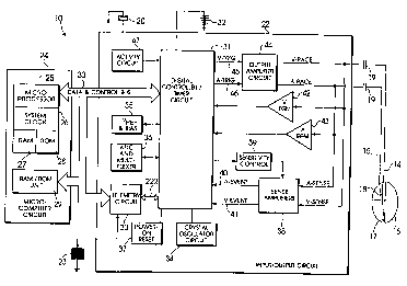
Referring to Figure 1, there is shown a block diagram
of an implantable pacemaker 10 which incorporates a telemetry
subsystem in accordance with the present invention. Although
the present invention will be described herein in conjunction
with a pacemaker 10 having a microprocessor-based architecture,
it will be understood that pacemaker 10 may be implemented in
any logic based, custom integrated circuit architecture, if
desired. The pacemaker shown in Figure 1 is substantially
similar to that disclosed in U.S. Patent No. 5,271,395 issued
on December 21, 1993 to Wahlstrand et al. entitled "Method and
Apparatus for Rate-Responsive Cardiac Pacing".
Although a particular implementation of a pacemaker
is disclosed herein, it is to be understood that the present
CA 02164963 2000-08-21
66742-539
8e
invention may be advantageously practiced in conjunction with
many different types of pacemakers, such as the pacemaker
described in the above-referenced Sivula et al. patent, for
example, as well as other types of implantable medical devices.
In Figure 1, pacemaker 10 is shown to include an
activity sensor 20, which may be, for example, a piezoelectric
element bonded to the inside of the pacemaker's shield. Such a
pacemaker/activity sensor configuration is the subject of the
above-referenced patent to Anderson et al. Piezoelectric
sensor 20 provides a sensor output which varies as a function
of a measured parameter that relates to the metabolic
requirements of a patient.
Pacemaker 10 of Figure 1 is programmable by means of
an external programming unit (not shown in Figure 1). One such
programmer suitable for the purposes of the present invention
is the Medtronic Model 9760 programmer which is commercially
available and is intended to be used with all Medtronic
pacemakers. The 9760 programmer is a microprocessor-based
device which provides a series of encoded signals to pacemaker
10 by means of a programming head which transmits radio-
frequency (RF) encoded signals to pacemaker 10 according to the
telemetry system laid out, for example, in U.S. Patent No.
5,127,404 to Wyborny et al. entitled "Improved Telemetry
Format", which is assigned to the assignee of the present
invention. It is to be understood, however, that the
programming methodology disclosed in the above-referenced
patent is identified herein for the purposes of illustration
only, and that any programming methodology may be employed so
long as the desired information can be conveyed between the
pacemaker and the external programmer.
66742-539
CA 02164963 2000-08-21
8f
It is believed that one of skill in the art would be
able to choose from any of a number of available pacemaker
programmers and programming techniques to accomplish the tasks
necessary for practicing the present invention. As noted
above, however, the Medtronic Model 9760 programmer is
presently preferred by the inventors.
In the illustrative embodiment of the present
invention, parameters such as the lower rate of pacemaker 10
may be programmable, for example from 40 to 90 pulses per
minute (PPM) in increments of 10 PPM, and the upper rate may be
programmable, for example, between 100 and 175 PPM in 25 PPM
WO 95100202; PCT/LTS94/05179
increments. There may also be programmable rate response functions in
pacemaker 10.
Pacemaker 10 is schematically shown in Figure 1 to be electrically coupled
via pacing lead 14 and 15 to a patient's heart 16. Leads 14 and 15 include one
or more intracardiac electrodes, designated as 17 and 18 in Figure 1, located
near their distal ends of leads 14 and 15, respectively, and positioned within
the
right vE:ntricular (R~ and right atrial (RA) chambers, respectively, of heart
16.
Leads 14 and 15 can be of either the unipolar or bipolar type as is well known
in
the artq alternatively, a single, multiple-electrode lead may be used.
lrlectrodes 17 and 18 are coupled via suitable lead conductors through
input capacitors 19 to input/output terminals of an input/output circuit 22.
In
the presently disclosed embodiment, activity sensor 20 is bonded to the inside
of
the pacemaker's outer protective shield, in accordance with common practice in
the art. As shown in Figure 1, the output from activity sensor 20 is also
coupled
to input/output circuit 22.
Input/output circuit 22 contains the analog circuits for interface to the
heart 16, activity sensor 20, an antenna 23, as well as circuits for the
application
of stimulating pulses to heart 16 to control its rate as a function thereof
under
control of the software-implemented algorithms in a microcomputer circuit 24.
Microcomputer circuit 24 comprises a microprocessor 25 having an
internal system clock circuit 26, and on-board RAM 27 and ROM 28.
Microcomputer circuit 24 further comprises a RAM/ROM unit 29.
Microprocessor 25 and RAM/ROM unit 29 are each coupled by a data and
control bus 30 to a digital controller/timer circuit 31 within input/output
circuit
22. Microcomputer circuit 24 may be a commercially-available, general-purpose
microprocessor or microcontroller, or may be a custom integrated circuit
device
augmented by standard RAM/ROM components.
lft will be understood that each of the electrical components represented in
Figure 1 is powered by an appropriate implantable battery power source 32, in
accordance with common practice in the art. For the sake of clarity, the
coupling
of battery power to the various components of pacemaker 10 has not been shown
in the Figures.
CA 02164963 2000-08-21
An antenna 23 is connected to input/output circuit ZZ for purpoxs of
uplink/dovvnlink telemetry through an RF telemetry circuit 33 in accordance
with
one embodiment of the imrention, to be hereinafter described in greater
detail.
In the embodiment of Figure 1, telemetry circuit 33 is coupled to digital
5 oontroller/timer circuit 31. It is contemplated that telemetry circuit 33
may also
be coupled directly to microcomputer circuit 24 via data and control bus 30.
A crystal oscillator circuit 34, typically a 32,768-Hz crystal-controlled
oscillator, provides main timing clock signals to digital controller/timer
circuit 31.
A V~, and Bias circuit 35 generates stable voltage reference and bias currents
10 for the analog circuits of input/output circuit 22. An analog-to-digital
comrerter
(ADC) and multiplexer unit 36 digitizes analog signals and voltages to provide
"real-time" telemetry intracardiac signals and battery end-of life (EOL)
replacement function. A power-on-rext (POR) circuit 37 functions as a means
to rext circuitry and related functions to a default condition upon detection
of a
low battery condition, which will occur upon initial device power-up or will
transiently occur in the prexacx of electromagnetic interference, for example.
The operating commands for controlling the timing of pacemaker 10 are
coupled by bus 30 to digital controller/timer circuit 31 wherein digital
timers and
counters are employed to establish the overall escape interval of the
pacemaker,
as well as various refractory, blanking, and other timing windows for
controlling
the operation of the peripheral components within input/output circuit 22.
Digital oontroller/timer circuit 31 is coupled to xnsing circuitry including
a xnse amplifier circuit 38 and a xnsitivity control circuit 39. In
particular,
digital oontroller/timer circuit 31 receives an A EVE1VT (atrial.event) signal
on
line 40, and a V EVENT (ventricular event) signal on line 41. Sense amplifier
circuit 38 is coupled to leads 14 and 15, in order to receive the V-SENSE
(ventricular sense) and A-SENSE (atrial sense) signals from heart 16. Sense
amplifier circuit 38 asxrts the A-EVENT signal on line 40 when an atrial event
(i.e., a paced or intrinsic atrial event) is detected, and asserts the V-EVENT
signal on line 41 when a ventricular event (paced or intrinsic) is detected.
Sense
amplifier circuit 38 includes one or more xnse amplifiers corresponding, for
example, to that discloxd in U.S. Patent No. 4,379,459 issued to Stein on
April
12, 1983
CA 02164963 2000-08-21
66742-539
11
Sensitivity control 39 is provided to adjust the gain
of sense amplifier circuitry 38 in accordance with programmed
sensitivity settings, as would be appreciated by those of
ordinary skill in the pacing art.
A V-EGM (ventricular electrocardiogram) amplifier 42
is coupled to lead 14 to receive the V-SENSE signal from heart
16. Similarly, an A-EGM (atrial electrocardiogram) amplifier
43 is coupled to lead 15 to receive the A-SENSE signal from
heart 16. The electrogram signals developed by V-EGM amplifier
42 and A-EGM amplifier 43 are used on those occasions when the
implanted device is being interrogated by external programmer
11, to transmit by uplink telemetry a representation of the
analog electrogram of the patient's electrical heart activity,
such as described in U.S. Patent No. 4,556,063, issued to
Thompson et al., assigned to the assignee of the present
invention.
Digital controller and timer circuit 31 is coupled to
an output amplifier circuit 44 via two lines 45 and 46,
designated V-TRIG (ventricular trigger) and A-TRIG (atrial
trigger), respectively. Circuit 31 asserts the V-TRIG signal
on line 45 in order to initiate the delivery of a ventricular
stimulating pulse to heart 16 via pace/sense lead 14.
Likewise, circuit 31 asserts the A-TRIG signal on line 46 to
initiate delivery of an atrial stimulating pulse to heart 16
via pace/sense lead 15. Output amplifier circuit 44 provides a
ventricular pacing pulse (V-PACE) to the right ventricle of
heart 16 in response to the V-TRIG signal developed by digital
controller/timer circuit 31 each time the ventricular escape
interval times out, or an externally transmitted pacing command
has been received, or in response to other stored commands as
CA 02164963 2000-08-21
66742-539
lla
is well known in the pacing art. Similarly, output amplifier
circuit 44 provides an atrial pacing pulse (A-PACE) to the
right atrium of heart 16 in response to the A-TRIG signal
developed by digital controller/timer circuit 31. Output
amplifier circuit 44 includes one or more output amplifiers
which may correspond generally to that disclosed in U.S. Patent
No. 4,476,868 issued to Thompson on October 16, 1984.
As would be appreciated by those of ordinary skill in
the art, input/output circuitry will include decoupling
circuitry for temporarily decoupling sense amplifier circuit
38, V-EGM amplifier 45 and A-EGM amplifier 46 from leads 14
WO 95/00202 PCT/US94105179
12
and 15 when stimulating pulses are being delivered by output amplifier circuit
44.
For the sake of clarity, such decoupling circuitry is not depicted in Figure
2.
While specific embodiments of sense amplifier circuitry, output amplifier
circuitry, and EGM amplifier circuitry have been identified herein, this is
done
for the purposes of illustration only. It is believed by the inventor that the
specific embodiments of such circuits are not critical to the present
invention so
long as they provide means for generating a stimulating pulse and provide
digital
controller/timer circuit 31 with signals indicative of natural and/or
stimulated
contractions of the heart. It is also believed that those of ordinary skill in
the art
could chose from among the various well-known implementations of such circuits
in practicing the present invention
Digital controller/timer circuit 31 is coupled to an activity circuit 47 for
receiving, processing, and amplifying activity signals received from activity
sensor
20. A suitable implementation of activity circuit 47 is described in detail in
the
atmve-referenced Sivula et al. application. It is believed that the particular
implementation of activity circuit 47 is not critical to an understanding of
the
present invention, and that various activity circuits are well-known to those
of
ordinary skill in the pacing art.
Referring to Figure 2, there is shown a block diagram of radio-frequency
(RF) telemetry subsystem 33 in accordance with one embodiment of the present
invention. Telemetry subsystem 33 of Figure 2 is coupled to antenna, 23, as
previously noted, for receiving RF signals from an external programming unit
(not shown in the Figures) such as the Model 9760 Programmer available from
Medtronic, line, Minneapolis, Minnesota.
In the presently preferred embodiment of the invention, the external
programmer transmits signals in the form of a series of short RF pulses. In
accordance with one aspect of the present invention to be hereinafter
described
in greater detail, telemetry system 33 of Figure 2 is capable of being readily
adapted for use in a variety of different telemetry schemes involving streams
of
RF pulses. In particular, it is believed the the telemetry system of Figure 1
may
be utilized in pulse position modulation, pulse width modulation, pulse
interval
modulation, and other types of telemetry protocols. In one embodiment to be
described herein in some detail, it will be assumed that a pulse interval
WO 95/00202 PCT/US94/05179
t~~.~~9fi~
13
. ,_ f;
modulation scheme will be supported, wherein the circuit of Figure 1
distinguishes between "0" data and "1" data based upon the duration of time
intervals between successive pulses received by antenna. 10. However, it is
believed by the inventors that those of ordinary skill in the art having the
benefit
of the present disclosure will be readily able to adapt the present invention
to be
used in support of other types of telemetry schemes, particularly those based
upon some form of pulse modulation.
As noted above, there are various pulse modulation schemes that may be
employed for the purposes of downlink telemetry. In one, called pulse interval
modulation, binary information is encoded such that the duration of the
interval
between RF bursts in the telemetry downlink signal is used to indicate the
type
of data (i.e., a zero or a one). In a variation of pulse interval modulation,
the
duration of the interval between successive trailing edges of RF bursts in the
downlink signal encodes the data.
The various downlink telemetry encoding protocols to be described herein
will perhaps best be appreciated with reference to Figure 3, which shows a
portion of one type of pulse interval modulated RF signal that may be received
by antenna 10.
The RF signal of Figure 3 consists of a stream of pulses of a 175-kHz (~
6-kHz) sinusoidal RF signal. In Figure 3, a first RF pulse, designated
generally
as 50, is called a "wake-up" or "start-of message" burst, and has a duration
of Tw
= 2000-Sec t 30-p~Sec. The wake-up burst 40 is issued to inform the telemetry
circuitzy that new data is to follow. Also shown in Figure 3 are a number of
"data bursts" designated generally as 52, 54, and 56.
In accordance with one telemetry protocol supported by the presently
disclosed embodiment of the invention, the telemetry circuitry must recognize
any burst within the range specified above for Tw (i.e., any burst with
duration
between 1970-uSec and 2030-uSec) as a start-of message, unless such burst
appears during a downlink message (i.e., from the time the telemetry circuit
first
recognizes a start-of message burst until it recognizes an end-of message
burst, to
be hereinafter described).
A message from the external unit is terminated with an "end-of message"
indicator, which comprises an interval T~ between any two consecutive trailing
WO 95/00202 PCT/US94/05179
14
edges of greater than 2440-~cSec. Thus, once the telemetry circuit has
recognized
a start-of message burst, any pause between trailing edges of consecutive
pulses
which exceeds 2440-~sSec is recognized as an end-of message indicator.
All downlink telemetry transmissions consists of a start-of message burst
followed by a number of data bursts, where the time between trailing edges of
data bursts indicates either a "0" bit or a "1'° bit. Alternatively,
the time between
the trailing edge of one burst and the rising edge of the next burst can be
used to
encode the data.
In Figure 3, the interval between the trailing edge of start-of message
burst 50 and the trailing edge of data burst 52 is designated as To. The time
interval between the trailing edge of data burst 42 and the trailing edge of
data
burst 54 is designated as Ti. The telemetry circuit in accordance with one
embodiment of the invention interprets the intervals between trailing edges as
follows: if the interval between trailing edges is in the range 900-~cSec ~30-
Sec,
this is interpreted as a "0" bit; similarly, if the range is in the range
2,200-Sec t
30-Sec, this is interpreted as a "1" bit.
Each data burst (such as 52, 54, and 56) in Figure 3 is specified to have a
duration of 200-~cSec ~ 50-~cSec. As would be appreciated by those of ordinary
skill in the art, if the duration of data bursts is known and consistent, then
the
above-described two types of pulse internal modulation (i.e., trailing-edge to
trailing-edge and trailing-edge to rising-edge) can be successfully
demodulated by
detecting and measuring the intervals between the trailing edge of one pulse
and
the rising edge of the next.
For the embodiment of the present invention shown in Figure 2, it will be
assumed that the above-described trailing-edge to trailing-edge pulse internal
modulation scheme is used for downlink telemetry. However, as will be apparent
to those of ordinary skill in the art, the system of Figure 2 to be
hereinafter
described in greater detail demodulates the pulse stream of Figure 3 on a
trailing-edge to rising-edge basis.
Signals consisting of a stream of RF bursts such as are depicted in Figure
3 are received by antenna 23 in the circuit of Figure 2, and are applied to an
RF
detect circuit 112 which converts the RF pulses in the antenna signal to
positive
logic square-wave pulses, in a conventional manner. In particular, RF detect
WO 95/00202 PCT/US94/05179
15 ~.~
circuit 112 may be as illustrated in the schematic diagram of Figure 4,
comprising
a diode 114, a capacitor 116 and resistor 118 coupled in parallel to ground,
and
two inverters 120 and 122. As would be appreciated by those of ordinary skill
in
the art, circuit 112 operates to produce a square-wave digital pulse output
signal
with positive-going pulses corresponding to RF bursts in the received RF
signal.
The square-wave digital pulse stream output signal derived by detect
circuit 112 is conveyed on line 124 to one input of an AND gate 126, one input
of a second AND gate 128, one input of a wake-up burst detect circuit 130, and
one input of a NOR gate 132. The signal on line 124 is also applied to the
RESET input of an N-bit counter 134.
Wake-up burst detect circuit functions to de-assert its output signal on line
156 upan detection of an RF burst of sufficient duration to qualify as a wake-
up
burst according to the protocol described above with reference to Figure 3.
The
output signal on line 156 from wake-up burst detector 130 is applied to a
second
input of NOR gate 132.
The output of NOR gate 132 is applied to the ENABLE input of a clock
circuit 136. Clock circuit 136 is enabled by a high logic level signal applied
to its
ENABLE input and, when enabled, produces a 4-kHz clock signal on line 138.
The clock signal on line 138 is applied to the clock inputs of N-bit counter
134,
and to the clock input of an M-bit flip-flop array 148.
gn accordance with an important aspect of the present invention, telemetry
circuit 33 of Figure 2 also includes a programmable logic array (PLA) 150. As
would be appreciated by those of ordinary skill in the art, a PLA is an array
of
switching elements that can be programmed to allow implementation of sum-of
products expressions. In general, a PLA has a plurality of input variables and
a
pluralit3r of output variables. Each function is realized as a sum of product
terms
involving the input variables. The variables are presented to a PLA in true
and
complemented form to an AND array in the PLA, where a plurality of product
terms are formed. These are then gated to an OR array in the PLA, where the
output functions are formed.
In the circuit of Figure 2, the variables applied to PLA 150 are supplied
from N-bit counter 134 and from M-bit flip-flop array 148. As shown in Figure
2, each of the output signals from counter 134 and flip-flop array 148 are
applied
WO 95/00202 PCT/US94/05179
.a 16
to an inverter array 152 so that both true and complemented forms of the
signals
can be supplied to PLA 150. PLA 150 is programmed such that certain
combinations of input signals cause corresponding output signals to be
asserted.
One of the output lines from PLA 150, designated as 154 in Figure 2, is
applied to a second input of wake-up detector circuit 130. When the signal
from
PAL 150 on line 154 is asserted, this causes wake-up detector circuit 130 to
assert its output signal on line 156, such that the output from NOR gate 132
is
deasserted, thereby disabling clock 136.
Another of the output lines from PLA 150, designated as 158 in Figure 1,
is applied to a second input of AND gate 126. Yet another of the output lines
from PLA 150, designated as 160, is applied to a second input of AND gate 128.
The output of AND gate 126 is applied to a "reset" (R) input of an RS
flip-flop 162, while the output from AND gate 128 is applied to the "set" (S)
input of flip-flop 162. The output from AND gates 126 and 128 are also each
applied to an input of a NOR gate 164. The output from NOR gate 164 is
applied to the SHIFT CLOCK input of an eight-bit serial-in/parallel-out shift
register 166. The output (Q) from RS flip-flop 162 is applied to the shift
data
input to shift register 166.
Operation of the circuit of Figure 2 as thus far described will perhaps best
be explained with reference to the timing diagram of Figure S.
In Figure 5, the binary value appearing at the outputs of counter 134 are
represented by the waveforms COUNTER BfT 0 (LSB), COUNTER BIT 1,
COUNTER BIT 2, and COUNTER BIT 3 (MSB). These values are applied via
inverter array 152 to the variable inputs of PLA 150. The waveform designated
RF SIGNAL in Figure 5 represents the RF signal received by antenna 23 in the
circuit of Figure 1. The waveform designated RF DETECT represents the
output of RF detect circuit 112, which waveform is present on line 124 in
Figure
2. The waveform WAKE UP in Figure 5 represents the output of wake-up burst
detector circuit 130, which is applied to one input of NOR gate 132 on line
156.
The waveform CLOCK ENABLE in Figure 5 represents the output of NOR gate
132; when asserted, this signal enables clock 136. The waveform DISABLE
DOV~I~tLIfNI~ represents the output on line 154 from PLA 150; when asserted,
(i.e., at a high logic level), the output from NOR gate 132 is prevented from
WO 95/00202; PCT/US94/05179
17, ;
going to a high logic level, thus preventing clock 136 from being enabled. The
waveforms "0" and '°1" in Figure S represent the output signals on
Lines 160 and
158, respectively, from PLA 150. The waveform RESET SHAT DATA IN
represents the output from AND gate 126 in Figure 2, while the waveform SET
SHIFT DATA IN represents the output from AND gate 128. The waveform
SHIFT DATA IN represents the output from RS flip-flop 162. Finally, the
wavefoi-m SHIFT CLOCK in Figure 5 represents the output from NOR gate 164.
Referring to Figures 1 and 5, the RF SIGNAL from antenna 23 is
converted to the RF DETECT signal by RF detect circuit 112. Note from Figure
5 that the output from wake-up burst detect circuit 130 on line 156 is
initially at
a high logic level. In Figure 5, a wake-up burst appears on the RF DETECT
line 124 beginning at time TO and ending at time Tl. As previously noted, when
a wake-up burst is detected in the output pulse stream from RF detect circuit
112
appears. on line 124, wake-up burst detect circuit 130 deasserts its output.
Thus,
at time Tl in Figure 5 when the RF DETECT signal makes a transition from a
high to a low logic level, the CLOCK ENABLE output from NOR gate 132
makes a low to-high transition, thereby enabling clock 136.
As would be apparent to those of ordinary skill in the art, the
arrangement of clock 136 and counter 134 is such that counter 134 functions to
count 4-kHz clock cycles from clock 136. Counter 134 is initially reset by
wake-
up burst in the RF DETECT signal; therefore at time T1, counter 134 begins
counting from zero, and continues counting until time T2, when the RF
DETECT signal rises. Thus, counter 134 effectively counts during the interval
from the falling edge of the RF DETECT signal at time Tl until the rising edge
of the RF DETECT signal at time T2, and the count value of counter 34 reflects
the duration of this interval. That is, the count value represents the number
of
244-~cSec intervals occurring while clock 134 was enabled.
During the interval between times T2 and T3 in Figure 5, another RF
pulse is received by antenna 23 and converted into a logic pulse in the RF
DETECT waveform. The high logic level of the RF DETECT signal during the
pulse between times T2 and T3 causes counter 134 to be reset, since the RF
DETECT signal is applied to the RESET input of counter 134. At time T3,
when the RF DETECT pulse ends, clock 36 is once again enabled, due to the
WO 95/00202 PCT/C1S94/05179
2~.6~~~3
1s
operation of NOR gate 132 as before. Thus, during the time interval between
times T3 and T6, clock 36 is enabled and clock cycles are counted by counter
134.
At time T6, another RF burst is received by antenna 23, causing another
data pulse in the RF DETECT waveform. Counter 34 is again reset, and at time
T7 when the data pulse ends, clock 136 is enabled and counter 134 counts clock
cycles.
The data pulse between times T6 and T7 resets counter 134, and at time
T7, clock 36 is enabled.
As previously noted, the downlink telemetry encoding scheme for the
presently disclosed embodiment of the invention is a variety of pulse interval
modulation, in which the time between trailing edges of data pulses is used to
indicate either "0" or "1" data. The start of data transmission is indicated
by a
°'wake-up" pulse, which in the timing diagram of Figure 5 is the long
pulse
designated generally as 172 in the RF SIGNAL waveform, during the interval
between times TO and Tl. In Figure 5, the time interval between the trailing
edge of the RF SIGNAL at time Tl and the trailing edge of the RF SIGNAL at
time T3 indicates a "0" data bit; the time interval between the trailing edges
of
the RF SIGNAL at times T3 and T7 indicate a "1" data bit. Since the data
pulses, such as the one occurring in the RF SIGNAL between times T2 and T3,
must be of a specified duration, the trailing-edge to trailing-edge encoding
can
also be interpreted by measuring the duration between the trailing edge of one
pulse and the rising edge of the next pulse (e.g., the time interval between
the
trailing edge of the wake-up burst at time Tl and the rising edge of the data
pulse at time T2).
As described above, counter 134 is operated to count during the time
interval between the trailing edge of one pulse and the rising edge of the
next
pulse. Thus, the counter value after each time counter 134 has been enabled
and
then disabled reflects this trailing-edge to rising-edge time interval. That
is, for a
longer trailing-edge to rising-edge time interval, the counter value of
counter 134
will be greater than for a shorter trailing-edge to rising-edge time interval.
Thus,
a correspondence can be established between counter values and intervals in
the
RF SIGNAL stream.
WO 95/00202; PCT/CTS94105179
.;
19
In accordance with the present invention, PLA 150 is programmed to
interpr et different counter values as indicating different conditions. In
particular,
PLA 50 is programmed such that when counter 134 is allowed, by virtue of its
being enabled and disabled as just described, to reach certain values, PLA 150
S interprets the counter values as indicating received data bits. The
correspondence between counter values and interpretation by PLA 150 is set
forth in the following Table 1:
TABLE 1
COUNTER REALrTIME INTERPRETA
VALUES VALUE TION
3 - 4 732 - 976 ~cSec "0" bit
9 - 10 2196 - 2440 ~cSec"1" bit
As set forth in Table 1, when counter 134 presents a value of three to the
inputs of PLA 150, PLA 150 asserts its "0" output on line 158; likewise, when
counter 134 presents a value of nine to the inputs of PLA 150, PLA 150 asserts
its "1" output on line 160.
With continued reference to Figures 2 and 5, the "0" output from PLA 150
on line 158 is combined with the RF DETECT signal by AND gate 126. As
would be appreciated by those of ordinary skill in the digital circuit art,
then, if
the "0" output from PLA 150 is asserted when the RF DETECT signal is
asserted, the output from AND gate 126 will be asserted as well. On the other
hand, if the RF DETECT signal is not asserted when the "0" output from PLA
150 is asserted, the output from AND gate 126 will remain at a low logic
level.
Similarly, the "1" output from PLA 150 is ANDed with the RF DETECT
signal by AND gate 128, so that if the RF DETECT signal is asserted when the
"1" output on line 160 from PLA 150 is asserted, the output from AND gate 128
will also be asserted.
Asserting the output of AND gate 126 causes RS flip-flop 162 to be reset
to a low logic output level. Asserting the output of AND gate 128 causes RS
flip-flop 162 to be set to a high logic output level.
WO 95/00202 PCT/US94/05179
~~.6~~6~ 2°
In the timing diagram of Figure 5, the interval between times T1 and T2
has a trailing-edge to rising-edge duration corresponding to a "0" in the
received
RF pulse stream. Thus, at time T2, counter 134 will have counted three cycles
of
the 4-kHz clock signal on line 158 and will therefore be presenting a counter
value of three (i.e., binary 1 1 0 0, LSB to MSB) to the inputs of P1:.A 150;
this is
reflected in the waveforms COUNTER BIT 0 (LSB), COUNTER BIT 1,
COUNTER BTT 2, and COUNTER BIT 3 (MSB) at time T2 in Figure 5; in
particular, at time T2, counter 134 has reached a count value of three (binary
1 1
0 0). PLA 150 is programmed such that a value of three applied to its inputs
results in assertion of the "0" output on line 158. As the "0" output on line
158 is
asserted at time T2, the RF DETECT output from RF detect circuit 112 will rise
to a high level, since the RF signal received by antenna 23 undergoes another
RF
burst beginning just after time T2. Thus, immediately after time T2, the RF
detect signal on line 124 and the "0" output on line 158 will be
simultaneously
asserted, thereby asserting the output of AND gate 126 to reset flip-flop 162.
Assertion of the output from AND gate 126 also causes the normally
asserted SHIFT DATA IN output of NOR gate 164 to be deasserted. This
falling edge of the output from NOR gate 164 causes the logic level appearing
at
the output of flip-flop 162 to be shifted into shift register 166.
Thus, the following chain of events occurs beginning at time T0: Between
times TO and Tl, a wake-up burst occurs, which is detected by wake-up burst
detector 130. When the RF DETECT signal goes to a low logic level at time Tl,
clock 136 is enabled so that between times Tl and T2, counter 134 is allowed
to
count up to a value of three. This causes PI:.A 150 to assert its "0" PLA
output
on line 158 at time T2. At time T2, the RF DETECT signal on line 124 rises
aad is ANDed with the "0" output on line 158. The ANDing of the RF DETECT
signal and the "0" output on line 124 results in assertion of the output from
AND
gate 126, which resets flip-flop 162 and causes the output of flip-flop 162 to
be
shifted into shift register 166. Since the assertion of the output from AND
gate
126 resets flip-flop 162, a low logic level (i.e., a zero) is shifted into
shift register
166.
WO 95/00202 ~ PCT/LTS94/05179
21 ~: ~~ -~ ; :-~
The assertion of the RF DETECT signal on line 124 at time T2 causes
counter 134 to be reset to a zero value in preparation for counting during the
next trailing-edge to rising-edge interval in the RF DETECT signal.
In Figure 5, the time interval between time T3 and TS represents the
trailing-edge to rising-edge interval for a "1" being transmitted. As before,
clock
136 is enabled beginning at time T3, due to the low logic level signal of the
RF
DETECT signal being applied to NOR gate 132. Counter 134 counts clock
cycles on line 138 throughout the entire interval between times T3 and T5. At
time T4, counter 134 reaches a count value of three, which could represent a
"0"
in the pulse stream, as just described. The count value of three being applied
to
the inputs of PLA 150 causes PLA 150 to assert its "0" output on line 158 at
time
T3 as before. However, at time T3 the RF DETECT signal on line 124 has not
risen to a high logic level as was the case at time T2. Therefore, assertion
of the
"0" output on line 158 does not cause the RESET SHIFT DATA IN output from
AND gate 126 to be asserted, and furthermore does not cause the SHIFT DATA
IN out)~ut from NOR gate 164 to be asserted.
At time T5, on the other hand, counter 134 reaches a value of nine, as
shown, this value corresponding to a received "1" as described with reference
to
Table 1 above. The count value of nine being applied to the inputs of PLA 150
at time TS causes PLA 150 to assert its "1" output on line 160. Also, just
after
time T.o, the RF DETECT signal on line 124 rises to a high level, as shown in
Figure 5. The RF DETECT signal on line 124 and the "1" output from PLA 150
on line 160 are ANDed at AND gate 128. The assertion of the output signal
from AND gate 128 (the SET SHIFT DATA IN signal) causes flip-flop 162 to be
set. Also, assertion of the SET SHIFT DATA IN signal from AND gate 128
causes the SHIFT DATA IN output from NOR gate 164 to be deasserted,
causing the output logic level from flip-flop 162 to be shifted into shift
register
166. Snnce flip-flop 162 was set by AND gate 128, in this case a "1" is
shifted into
shift register 166 just after time T5.
'The RF DETECT signal on line 124 rising after time T5, resets counter
134 and disables clock 136. At time T6, the RF DETECT signal on line 124
falls, beginning another interval corresponding to a "0" in the transmitted RF
burst stream. As before, clock 136 is enabled at time T6 and counter 134
begins
WO 95/00202 PCT/LTS94/05179
22
counting clock cycles. At time T7, counter 134 will have again reached a count
value of three, causing the "0" output on line 158 from PLA 150 to be
asserted.
The °'0" output is ANDed with the RF DETECT signal (asserted just
after time
T7) at AND gate 126, resetting flip-flop 162 and initiating a shift clock
pulse to
shift register 166. Thus, another "0" is shifted in to shift register 166.
Begisnning at time T8, no further RF bursts appear in the RF SIGNAL.
Counter 134, which is reset after time T7 and enabled at time T8 when the RF
DETECT signal falls, begins counting clock cycles at time T8. At time T9,
counter 134 reaches a count value of three and PLA 150 therefore asserts its
"0"
output signal. However, since the RF DETECT signal does not rise at time T9,
no SHIFT DATA IN pulse is generated, and no data is shifted into shift
register
166. Similarly, at time T10, counter 134 reachs a count values of nine and PLA
therefore asserts its "1" output on line 160. Again, however, since the RF
DETECT signal does not rise at time T10, no SHIFT DATA IN pulse is
generated and no data is shifted into shift register 166.
Counter 134 reaches a count value of ten at time Tll in Figure 5. PLA
150 is programmed such that it asserts the DISABLE DO~ signal on line
154 whenever a value of ten is applied to its inputs. Thus, whenever the RF
DETECT signal remains at a low logic level for ten clock cycles (i.e., 2440-
Sec),
the DISABLE DOW1VLINK signal on line 154 is asserted. Assertion of the
DISABLE DOVi~NLINI~ signal causes wake-up burst detect circuit 130 to assert
its output on line 156, thereby preventing clock 136 from being enabled.
Thereafter, counter 134 will have no clock cycles to count, and no outputs
from
PLA 150 will be asserted. Downlink telemetry is thus disabled, until another
wake-up burst is detected.
In the embodiment of the invention depicted in Figure 2, downlink
telemetry data is demodulated as just described. A downlink telemetry format
for the pulse-interval modulation protocol described with reference to Figure
3 is
shown in Figure 6. In particular, a downlink message to device 10 begins with
a
wake-up burst, designated as 172 in Figure 6, followed by five eight-bit
bytes,
each having a predetermined meaning. A first byte following wake-up burst 172,
comprises an eight-bit access code for preventing inadvertent activation of
telemetry system 33. A second byte following wake-up burst 172 contains eight
WO 95/00202 PCT/CTS94/05179
..
23
bits of control information. A third byte contains address information
identifying
the type of information being transmitted, while a fourth byte contains the
information value. Finally, eight bits at the end of the downlink message are
used as check bits (e.g., parity bits) for detection/correction of errors in
the
downlink message.
As would be appreciated by those of ordinary skill in the art, the precise
length of a downlink message having the format shown in Figure 6 will vary
depending upon the proportion of zeros and ones transmitted, since the
modulating interval for a one is longer than that for a zero. Assuming an
average of one-half zeros and one-half ones in the downlink message shown in
Figure 6, the entire message takes approximately 60-mSec to transmit.
'Telemetry subsystem 33 of Figure 2 is also employed in uplink telemetry,
i.e., information transmitted from implanted device 10 to an external
receiving
device. In accordance with common practice in the industry, the modulation
scheme employed for uplink telemetry is not the same as the pulse-interval
modulation scheme described above for downlink telemetry. In the presently
disclosed embodiment of the invention, uplink telemetry data is modulated
using
a pulse-position modulation technique, wherein a message frame is divided into
a
plurality of time slots, and wherein data is represented by either the
presence or
absencx of an RF burst in each time slot.
llZeferring to Figure 7, there is shown a data frame for the uplink
telemetry protocol in accordance with the presently disclosed embodiment of
the
invention. The data frame of Figure 7 consists of 64 separate time slots, each
having a duration of 30.5-~cSec. During uplink telemetry, an RF burst may or
may not occur in each time slot in the frame of Figure 7. An RF burst during a
time slot represents a "1", while the absence of an RF burst during a time
slot
represents a "0". Each frame begins with an RF burst in time slots 0 and 4,
with
no RF bursts in time slots 1, 2, 3, 5, 6, 7, or 8. The RF bursts in time slots
0 and
4 are used for synchronization of the uplink telemetry transmitter and
receiver.
lLn the eleven time slots 9 through 19, designated collectively as 200 in
Figure 7, data representing a telemetry channel identifier is transmitted. In
the
presently disclosed embodiment of the invention, telemetry circuit 33 may be
employed to provide a number of separate telemetry channels between implanted
WO 95/00202 PCT/US94/05179
24
device 10 and an external receiver. In particular, there are five different
telemetry channels supported by telemetry circuit 33: an Idle channel, used
for
maintaining a telemetry link without communicating data between the implanted
device and the external unit; a Waveform channel, for communicating digitized
analog data; a Message channel, for communicating messages; a Marker channel,
for communicating, in real time, "event markers" representing the occurrence
of
different cardiac events (see the above-reference Markowitz '382 patent); and
a
Handshake channel, for establishing a telemetry link between an implanted
device and an external programming unit.
Time slots 24 through 39 in the uplink telemetry frame of Figure 7,
designated collectively as 202 therein, are used to encode the low order
nibble
(four bits) of a byte of data transmitted by telemetry system 33. As would be
appreciated by those of ordinary skill in the art, there are sixteen possible
nibbles
-- i.e., sixteen different combinations of four binary digits: 00~, 0001,
0010, ...
1111. In accordance with the presently disclosed embodiment of the invention,
each of the sixteen positions in the low order nibble section of the uplink
telemetry data frame corresponds to one possible nibble. Thus, for example, an
RF pulse in time slot 24 of the uplink telemetry data frame of Figure 7 (i.e.,
the
first time-slot in low-order nibble section 202) may be defined to correspond
to
the nibble 0000, position, time slot 25 may be defined to correspond to the
nibble
0001, and so on, time slot 39 (the last time slot in low-order nibble section
202)
corresponding to the nibble 1111. With such an encoding scheme, an RF burst
will occur in one and only one time slot in the low-order nibble section of
the
frame of Figure 7.
Time slots 44 through 59 in the uplink telemetry frame of Figure 7,
designated collectively as 204, are used to encode the high-order nibble of a
byte
of uplink telemetry data. As with low-order nibble section 202 of the frame of
Figure 7, each of the sixteen time slots in high-order nibble section 204 are
used
to identify one of the sixteen possible high-order nibbles. Thus, an RF burst
will
occur in one and only one of the time slots in high-order nibble section 204
of
the frame of Figure 7.
It is contemplated that the uplink telemetry frame of Figure 7 may further
include additional time slots (not shown in Figure 7) for encoding a "parity
WO 95/00202 PCT/US94/05179
2s
~~ ~~~~3
nibble", defined to be the bit wise exclusive-OR of the low-order and high-
order
data nibbles. For example, additional time slots 64 through 79 could be
defined
to encode the parity nibble. A parity nibble as just described is believed to
not
be essential to the practicing of the present invention, but would enhance the
telemetry system's noise immunity.
l:~urther in accordance with the present invention, the uplink telemetry
protocol defines an uplink telemetry record as comprising 37 frames of data,
where each frame has the format previously described with reference to Figure
7.
A diagram of a telemetry record in accordance with the presently disclosed
embodiment of the invention is provided in Figure 8. The 37 frames of data in.
the uplink telemetry record of Figure 8 are defined as follows: Frame 1,
designated as 206 in Figure 8, is an idle frame. Frame 2, designated as 208 in
Figure 8, is a frame used for identifying the model number of pacemaker 10.
Frame 3, designated as 210 in Figure 8, is a frame for communicating status
information in the uplink telemetry signal. Frame 4, designated as 212 in
Figure
8, contains error checking information for the record.
l~rames 5 through 37, designated collectively as 214, in the uplink
telemetry record of Figure 8 are used to transmit data- Thus, each uplink
telemetry record transmitted from device 10 contains four status/control
frames,
and thirty-three data frames, each containing one byte of data. An entire
uplink
telemetry record, consisting of 37 frames of data, takes just over 70-mSec to
transmit.
'lChe uplink telemetry protocol described herein with reference to Figures
7 and 8 is substantially similar to that disclosed in the above-reference
Wyborny
et al. patent.
In accordance with the presently disclosed embodiment of the invention,
uplink telemetry is accomplished using the same PLA 150 used for downlink
telemetry.
As described above with reference to downlink telemetry in accordance
with the presently disclosed embodiment of the invention, PLA 150 was
conventional in design and operation. However, for the purposes of uplink
telemetry, PLA 150 includes a RAM-programmable section 220 that is not used
for downlink telemetry. Section 220 of PlrA 150 is coupled to receive nibbles
of
WO 95/00202 PCTlUS94/05179
49 ~~
data in parallel form via an eight-bit bus 222 that is also coupled to the
respective bit positions of shift register 166. Bus 222 couples telemetry
system 33
to digital controller 31, as shown in Figure 2, or may couple telemetry system
33
directly to data and control bus 30 in device 10, so that bus 222 could be
used to
couple telemetry system 33 directly to microcomputer circuit 24. Whether
telemetry system 33 is coupled directly to microcomputer circuit 24 or
indirectly,
through digital circuit 31, is considered to be a design option which may be
exercised in various ways depending upon the particular implementation. For
the
purposes of the following description, it is sufficient to describe bus 222 as
coupling telemetry circuit 33 to some source of uplink telemetry data, whether
it
be microcomputer circuit 24 or digital controller circuit 31.
As shown in Figure 2, four bit lines of bus 222 control one output term
224 of PLA 150, while the remaining four bit lines of bus 222 control another
output term 226 of PLA 150. Programmable section 220 of PLA 150 is
controlled by means of a PROGRAM input signal to PLA 150, the PROGRAM
input signal being supplied from digital controller circuit 31 (or from
microcomputer circuit 34, depending upon the implementation). Programmable
section 220 of PLA 150 functions to latch the eight data bits on bus 222 into
the
eight locations in programmable section 220 corresponding to the output terms
224 and 226 upon assertion of the PROGRAM input signal. In this way, the
decode value for terms 224 and 226 can be dynamically reprogrammed during
uplink telemetry operation. Once programmed, output terms 224 and 226
behave as conventional output terms, asserting their respective outputs
whenever
input signals from counter 134 and flip-flop array 148 match the programmed
values in programmable section 220. In particular, the output lines from
programmable PLA terms 224 and 226 are coupled to the TELEMETRY OUT
output from PLA 150.
In Figure 9, there is shown one possible implementation of programmable
section 220 of PLA 150. The circuit of Figure 9 represents a single
programmable bit in programmable section 220. As in conventional PLA cells,
the programmable PLA cell of Figure 9 receives an input signal and its inverse
on lines designated 240 and 242. These signals are applied to the gates of
transistors 244 and 246, respectively. Coupled with transistor 244 is a second
WO 95/00202 PCT/US94/05179
~ 2~ X164963
transistor 248, and coupled with transistor 246 is a second transistor 250.
The
gates of transistors 248 and 250 are coupled to a latch comprising inverters
252
and 254; in particular, the gate of transistor 250 is coupled to the output of
inverter 254, while the gate of transistor 248 is coupled to the output of
inverter
252.
7Che state of the latch formed by inverters 252 and 254 is programmable
by means of the PROGRAM input signal, which is applied to the gate of a
transistor designated as 256 in Figure 9. When the PROGRAM signal is
asserted, transistor 256 is rendered conductive, thereby setting the state of
the
latch f~rmed by inverters 252 and 254 according to the signal then being
applied
to the DATA input in Figure 9. After the PROGRAM signal is deasserted, the
DATA value is latched in the cell.
Although a particular implementation of a programmable section of PLA
150 has been described herein in some detail, it is believed that an
equivalent
circuit could be implemented in any of various ways by persons skilled in the
art.
P:ach of the programmable output terms 224 and 226 in Figure 2
corresponds to four of the programmable PLA cells depicted in Figure 9. In
accordance with the presently disclosed embodiment of the invention, each byte
of uplink telemetry data to be transmitted from device 10 to an external
receiver
is first programmed into the eight programmable locations in programmable
section 220 of PLA 150.
For uplink telemetry, clock 136 generates a 32-kHz clock signal on line
138, whereas for downlink telemetry, clock 136 was described as a 4-kHz clock.
In one implementation of the present invention, a single 32-kHz clock 136 is
used, and a clock divider circuit, not shown in the figures, is used to derive
the 4-
kHz clock signal needed for downlink telemetry. It is also contemplated that
separate uplink and downlink telemetry clocks could be provided.
Alternatively,
a single 32-kHz clock could be employed, provided that PLA 150 was
reprogrammed with different downlink telemetry terms, since the number of
clock cycles in each trailing-edge to trailing-edge interval would be eight
times as
great for a 32-kHz clock as for a 4-kHz clock. The selection of one of these
design options is not believed to be critical to understanding or practicing
the
present invention.
WO 95/00202 PCT/US94/05179
Once a byte of uplink telemetry data has been programmed into the eight
programmable PLA cells of output terms 224 and 226, clock 136 is enabled by
assertion of the UPLINK ENABLE signal applied to the ENABLE input of clock
136. The UPLINK ENABLE signal is provided from digital controller/timer
circuit 31 (or directly from microcomputer circuit 24, as previously
described).
The 32-kHz clock signal on line 138 causes counter 134 to be incremented
once for each clock cycle. Each time the output from clock 134 matches an
output term in PLA 150, the output signal corresponding to that term is
asserted,
as in a conventional PLA.
As shown in Figure 2, a number of PLA outputs are fed back into three-
bit flip-flop array 148, on lines designated 262, 264, and 266. Similarly, one
PLA
output is fed back on line 260 to a RESET input to counter 134. Flip-flop
array
148 functions as a state register, and the contents of the state register 148
are
applied as input terms to PLA 150. Another output line from PLA 150,
designated as TELEMETRY OUT in Figure 2, is coupled to a telemetry driver
circuit (not shown). When a pulse is produced on the TELEMETRY OUT
output line, this pulse causes the telemetry driver circuit to "ring'°
the telemetry
coil, thereby producing an RF burst that is transmitted to the external
receiver.
As noted above, the PLA outputs corresponding to programmable terms 224 and
226 are coupled to the TELEMETRY OUT output line, so that when a match
between input terms from counter 134 and state register 148 and one of the
programmable terms 224 or 226 occurs, a telemetry pulse (RF burst) is
transmitted.
Another output from PLA 150 is designated with reference numeral 260 in
Figure 2 and is coupled to the RESET input to counter 134. Thus, a
correspondence between some term in PLA 150 and the inputs thereto will result
in counter 134 being reset, as will be hereinafter described in greater
detail.
Three other outputs from PLA 150, designated with reference numerals
262, 264, and 266 in Figure 2, are applied to the inputs of three flip-flop
state
register 148. As previously noted, the outputs from state register 148 are
applied
as inputs to PLA 150. This feed-back arrangement of output lines 262, 264 and
266 is such that the state variable stored in state register 148 can be set
according to correspondence between certain input combinations to PLA 150.
WO 95/00202 ~ ~~~ PCT/US94/05179
~~ ~~ ~ i ! _
29
Still another output from PLA 1$0, designated by reference numeral 268
in Figure 2, indicates when a frame of data has been transmitted. This signal
may be provided, for example, to microcomputer circuit 24 or microcontroller
circuit 22 to provide an indication that telemetry circuit 33 is ready for
further
$ uplink telemetry operation.
In the following Table 2, there is set forth the correspondence between
certain input terms and the behavior of PLA 1$0 in response thereto:
TABLE 2
=rmrrs oi rrpvTs
1~ sgg~t C3 C2 Cl CO SZ S1 80 OUTPnTS S2' Sl'SO'
EVER ASSERTED
1 0 0 0 0 0 0 ~ TELEMETRY 0 0 0
0
OUT
Z 0 1 0 0 0 0 0 TELEMETRY 0 0 0
OUT
3 1 0 0 0 0 0 0 RESET 0 0 1
COUNTER
1$ 4 (CHANNEL 0 0 1 TELEMETRY 0 0 1
ID)
OUT
S 1 0 1 1 0 0 1 RESET 0 1 0
COUNTER
6 0 1 0 0 0 1 0 RESET 0 1 1
COUNTER
7 (TERM 224) 0 1 1 TELEMETRY 0 1 1
OUT
8 0 0 0 0 0 1 1 RESET 1 0 0
COUNTER
20 9 0 1 0 0 1 0 0 RESET 1 0 1
COUNTER
(TERM 226) 1 0 1 TELEMETRY 1 0 1
OUT
il 0 0 0 0 1 0 1 RESET 1 1 0
COUNTER
12 0 1 0 0 1 1 0 END OF 0 0 0
FRAME
25 xn Table 2 above, the left half ("INPUTS") specifies a combination of
inputs, while the right half ("OUTPUTS") identifies what output lines are
asserted in response to the specified inputs. For example, term number 1 in
Table 2 indicates that when a counter value of zero (i.e., {C3 C2 Cl CO} _ {0
0
0 0~) and a state variable of zero (i.e., {S2 S1 SO} _ {0 0 0)) are applied to
the
WO 95/00202 PCT/US94/05179
inputs of PLA 150, TELEMETRY OUT is asserted, and the output signals on
lines 262, 264, and 266 (the "new state" variable) are at a low Iogic level.
Thus,
in response to the inputs Iisted in term number 1 in Table 2, an RF burst is
transmitted and the state machine remains in state zero (i.e., {S2' S1' S0'} _
{0
5 0 0} ).
Term number 2 in Table 2 indicates that when a counter value of four
(i.e., {C3 C2 Cl CO} _ {0 1 0 0}) and a state variable of zero are applied to
the
inputs of PLA 150, TELEMETRY OUT is asserted and the state machine
remains in state zero (i.e., the signals on lines 262, 264, and 266 are held
at a low
10 logic level).
Term number 3 in Table 2 indicates that when a counter value of eight
(i.e., {C3 C2 Cl CO} _ {0 0 0 0}) and a state variable of zero are applied to
the
input of PLA 150, the RESET COUNTER output on line 260 from PLA 150 is
asserted. Also, the "new state" state variable is set to a value of one (i.e.,
the
15 signals on lines 262, 264, and 266 are at high, low, and low logic levels,
respectively). Thus, in response to the input signal combination listed for
term
number 3 in Table 2, the state machine implemented by PLA 150 goes from
state zero to state one, and counter 134 is reset.
Term number 4 in Table 2 lists "Channel m" as the counter value input
20 term, and state one as the state register input term. In the presently
disclosed
embodiment of the invention, PLA 150 is programmed with one term for the
channel m value. Term 4 in Table 2 indicates that when the current state value
is one (i.e., {S2 S1 SO} _ {0 0 1}) and a match between the value from counter
134 and the channel m occurs, a telemetry pulse is generated by assertion of
the
25 TELEMETRY OUT signal.
Term number 5 in Table 2 indicates that when the current state value is
one and the value from counter 134 is eleven (i.e., {C3 C2 Cl CO} _ {1 0 1
1}),
counter 134 is reset by assertion of the signal on output line 260, and a new
state
value of two (i.e., {S2 Sl SO} _ {0 1 0}) is loaded into state register 148.
30 Term number 6 in Table 2 indicates that when the current state value is
two and the value from counter 134 is four, counter 134 is reset and a new
state
value of three is loaded into register 148.
WO 95/00202 PCT/US94/05179
31
Term number 7 in Table 2 indicates that when the current state value is
three and the value from counter 134 reaches the value programmed into
programmable term 224 in PLA 150, a telemetry pulse is generated; the state
value remains at three.
'Term number 8 in Table 2 indicates that when the current state value is
three and the value from counter 134 reaches zero (i.e., when the counter
increments from fifteen (1 1 1 1) to sixteen (0 0 0 0)), counter 134 is reset
and a
new state value of four is loaded into state register 148.
'Term number 9 in Table 2 indicates that when the current state value is
four and counter 134 reaches a value of four, counter 134 is reset and a new
state value of five is loaded into state register 148.
'Term number 10 in Table 2 indicates that when the current state value is
five and counter 134 reaches a value which matches the bits programmed into
programmable term 226 in PLA 150, a telemetry pulse is generated.
'term number 11 in Table 2 indicates that when the current state value is
five and counter 134 reaches zero (i.e., when counter 134 has counted to
sixteen,
as with term 8 above), counter 134 is reset and a new state value of six is
loaded
into state register 148.
lFinally, term number 12 in Table 2 indicates that when the current state
value is six and counter 134 reaches a value of four, the END OF FRAME
output signal on line 268 is asserted.
XJplink telemetry proceeds as follows: First, two nibbles of data, to be
transmitted in fields 202 and 204 of an uplink telemetry frame (see Figure 7)
are
programmed into programmable terms 224 and 226 of PLA 150. Then, the
UPLINK ENABLE signal is asserted, thereby allowing the 32-kHz clock signal
from clock 136 to be applied to the input of counter 134.
1~ounter 134 and state register 148 are initially set to zero; when clock 136
is enabled, counter 134 begins counting clock cycles. Before counter 134
increments from zero to one, however, the counter value will be zero and the
state value in register 148 will be zero. As indicated in term 1 of Table 2
above,
PLA 1S0 is programmed to respond to this condition (count = zero, state = 0)
by asserting the TELEMETRY OUT signal to initiate transmission of an RF
WO 95/00202 PCT/US94/O51'79
32
telemetry pulse. This pulse corresponds to the synchronization pulse in time
slot
0 of the uplink telemetry frame of Figure 7.
Counter 134 will next count clock pulses until it reaches a counter value of
four; the state value will still be zero. As indicated in term 2 of Table 2
above,
PLA 150 is programmed to respond to this condition (count = 4, state = 0) by
asserting the TELEMETRY OUT signal to initiate transmission of an RF
telemetry pulse. This pulse corresponds to the synchronization pulse in time
slot
4 of the uplink telemetry frame of Figure 7.
Counter 134 will continue counting clock pulses until it reaches a count
value of eight; the state value will still be zero. As indicated in term 3 of
Table
2 above, PLA 150 is programmed to respond to the condition (count = 8, state
= 0) to assert the signal on line 260, thereby resetting counter 134 to a zero
count value. Also, a new state value of one (i.e., ~S2 S1 SO} _ {0 0 1)) is
loaded into state register 148. This occurs at time slot eight in the uplink
telemetry frame of Figure 7.
With the state register now indicating to PLA 150 that the current state is
one, counter 134 will begin counting from zero. Thereafter, when the counter
value reaches the value corresponding to the current telemetry channel 1T~
value,
term 4 of Table 2 indicates that PLA 150 will initiate a telemetry pulse by
asserting the TELEMETRY OUT signal. This telemetry pulse occurs during the
C> :fANNEL m section 200 of the uplink telemetry frame of Figure 7, and its
position in section 200 identifies the channel that the current frame
corresponds
to.
After the channel m pulse is delivered, counter 134 will continue counting
until it reaches a value of eleven. As indicaxed by term 5 of Table 2 above,
PLA
150 is programmed to respond to this condition (count = 11, state = 1) to
reset
counter 134 and load a new state value of two into state register 148. This
occurs at time slot 19 in the uplink telemetry frame of Figure 7.
Counter 134 thus begins counting from zero, beginning with time slot 20
of the uplink telemetry frame of Figure 7. When counter 134 reaches a count
value of four, term 6 of Table 2 indicates that PLA 150 will respond by
asserting
the signal on line 260 to reset counter 134, and enter a new state value of
three
WO 95/00202 PCT/US94/05179
33 ~' ' '' :.
into state register 148. This occurs at time slot 23 in the uplink telemetry
frame
of Figure 7.
Counter 134 next begins counting from zero. As indicated by term 7 of
Table 2, when the count value of counter 134 reaches a value corresponding to
the data previously programmed into programmable term 224 of PLA 150, PLA
responds by asserting the TELEMETRY OIJT signal to initiate transmission of a
telemetry pulse. This pulse will occur during one of the time slots (24 - 39)
in
the low-order nibble section 202 of the uplink telemetry frame of Figure 7.
The
position of this pulse in section 202 of the frame corresponds to the
programmed
data value in term 224 of PLA 150. That is, assuming that the sixteen time
slots
in low-order nibble section 202 of the uplink telemetry frame are numbered
from
zero to~ fifteen, if a binary value of four is programmed into term 224 of PLA
150, a 'telemetry pulse will be transmitted in the fifth time slot (time slot
4) of
section 202 of the frame. A binary value of zero programmed into term 224 will
cause a telemetry pulse to be transmitted in the first time slot (time slot 0)
of
section 202.
After transmission of a pulse during one of the time slots in section 202 of
the data frame, counter 134 will continue counting until it reaches a count
value
of zero (i.e., when it increments from fifteen); the state value will still be
three at
this point. As indicated by term 8 in Table 2, PLA 150 is responsive to this
condition (count - 0, state = 3) to reset counter 134 and load a new state
value
of four into state register 148. This occurs at time slot 39 in the uplink
telemetry
data frame of Figure 7 (i.e., the last time slot in low-order nibble section
202 of
the data frame).
Now in state four, counter 134 will count until it reaches a value of four.
As indicated by term 9 of Table 2, when counter 134 reaches a count value of
four when in state four, PLA 150 responds by resetting counter 134 and loading
a
new state value of five into state register 148. This occurs in time slot 43
of the
uplink telemetry data frame of Figure 7.
In state five, counter 134 will begin counting from zero until its count
value snatches the value programmed into programmable term 226 in PLA 150.
At this point, PLA 150 will assert the TELEMETRY OUT signal to initiate
transmission of a telemetry pulse, as indicated by term 10 of Table 2. This
pulse
WO 95/00202 PCT/US94/05179
34
will be delivered during high-order nibble section 204 of the data frame of
Figure
7, and as with the pulse delivered during low-order nibble section 202, the
pulse
will be transmitted during the nth time slot of section 204 when a value of (n-
1)
is programmed into programmable PLA term 226.
After transmission of a telemetry pulse during one time slot of high-order
nibble section 204 of the data frame, counter 134 will continue counting until
it
reaches a zero value (i.e., after it increments from a value of fifteen). Term
11
of Table 2 indicates that in response to this condition (count = 0, state =
5),
PLA 150 will assert the signal on line 260 to reset counter 134, and will load
a
new state value of six into state register 148. This occurs at time slot 59 in
the
uplink telemetry frame of Figure 7, the last time slot in high-order nibble
section
204.
With the state machine in state six, counter 134 will begin counting from
zero until it reaches a value of four. According to term 12 of Table 2, PLA
150
will respond to this condition (count = 4, state = 6) by asserting the END OF
FRAME signal on line 268. This occurs at the last time slot in the uplink
telemetry frame of Figure 7.
As would be appreciated by those of ordinary skill in the art, telemetry
circuit 33 of Figure 2 can be configured to operate with many different types
of
telemetry formats by stepping from state to state via feedback state register
148.
All parameters of the telemetry protocol can be adjusted by specifying the
frequency of clock 136, the width of counter 134, the bit with of programmable
PLA terms 224 and 226 (and/or the inclusion of more than two programmable
nibbles in PLA 150), and the number of allowable state values. For both uplink
and downlink telemetry for the system of Figure 2, more than one telemetry
protocol can be programmed into a single PLA 150.
Turning now to Figure 10, there is shown a block diagram of a telemetry
subsystem 33' in accordance with another embodiment of the present invention.
As with telemetry system 33 of Figure 2, telemetry system 33' of Figure 10 is
a
PLA-based circuit operable in conjunction with an implantable device such as
the
pacemaker 10 of Figure 1.
Referring to Figure 10, telemetry circuit 33' includes a PLA 300, a five-bit
counter 302, a five bit state register 304, and an eight-bit shift register
306. For
WO 95/00202 ~ PCT/US94/05179
35 . ,
downlink telemetry, circuit 33' includes a falling edge detector and wake-up
burst
detector 308, coupled to receive a RF DETECT signal on line 310 from an RF
detect circuit 312. As with RF detect circuit 112 in the embodiment of the
invention shown in Figure 2, RF detect circuit 312 in circuit 33' of Figure 10
receives the received signal from antenna 23 and converts the stream of RF
pulses to a stream of digital logic pulses. Falling edge detector and wake-up
burst detector circuit 308 functions to assert an output signal on a first
output
line 314 upon detecting falling edge in the RF DETECT signal on line 310, and
further to assert an output signal on a second output line 316 upon detection
of a
wake-up burst in the RF DETECT signal, as previously described with reference
to Figure 3.
The signals on lines 314 and 316 indicating falling edges and wake-up
bursts, respectively, are applied to the inputs of a 2:1 multiplexer 318, the
output
of which is applied to a PLARF input to PLA 300. Thus, either the falling edge
signal on line 314 or the wake-up burst signal on line 316 can be applied to
the
PLARl~ input of PLA 300, depending upon the logic level of a control signal
applied on line 320 to the control input of multiplexer 318. The signal on
line
320 is derived from one bit of five-bit state register 304; in particular, the
signal
on line 320 reflects the fifth state bit, ST < 4 > .
.All five state register bits ST < 4:0 > are applied via bus 322 to a STATE
input of PLA 300.
'The five bits CNT < 4:0 > reflecting the count value of counter 302 are also
applied as inputs to PLA 300, on bus 324. Bus 324 also conveys four of the
count bits, CNT < 3:0 > to a four-bit input of a comparator 326. Another input
of
four-bii: comparator 326 receives four signals on bus 328 from the output of a
4x4:1 multiplexer 330. The output of comparator 326 is conducted on line 332
to
a MATCH input to PLA 150. The signal on line 332 is asserted when the four
count value bits CNT < 3:0 > on bus 324 are found to match the four bits on
line
328 supplied from multiplexer 330.
lEight bits of data from the eight positions SR < 7:0 > of shift register 306
are presented on eight-bit bus 334. Four of the shift register bits, SR < 3:0
>, are
applied to a first four-bit input (00) of multiplexer 330. The remaining four
bits
SR < 7:4 > are applied to a second four-bit input (10) of multiplexer 330. All
WO 95/00202 PCT/US94/05179
36
eight shift register bits SR < 7:0 > are applied to an input of a CPU
transmit/receive buffer 336.
As shown in Figure 10, the first four shift register bits SR < 3:0 > and the
second four shift register bits SR < 7:4 > are applied to separate inputs of a
four-
bit exclusive-or (4xXOR) circuit 338. 4xXOR circuit 338 performs a bit-wise
logical exclusive-or function on the shift register bits; that is, bit SR < 7
> is
exclusive-ORed with bit SR < 3 > , bit SR < 6 > with bit SR < 2 >, bit SR < 5
> with
bit SR < 1 >, and bit SR < 4 > with bit SR < 0 > . The four exclusive-or
results are
then applied to a third four-bit input (11) of 4x4:1 multiplexer 330. 4xXOR
circuit 338 is employed to provide the "parity nibble" for an uplink telemetry
frame, as previously described with reference to Figure 7.
As shown in Figure 10, telemetry circuit 33' in accordance with the
presently disclosed embodiment of the invention is preferably coupled directly
to
data and control bus 30 of microcomputer circuit 24., although as with the
embodiment of Figure 2, it is contemplated that circuit 33' may be coupled to
microcomputer circuit indirectly, via digital controller/timer circuit 31.
As previously noted, pacemaker 10 from Figure 1 preferably supports a
plurality of different telemetry channels (e.g., Idle, Waveform, Message,
Marker,
and Handshake). A different uplink telemetry frame may be defined for each
different channel. In order to identify to PLA 300 what channel an uplink
message is to be transmitted on (and thus what type of uplink frame to
transmit),
two signals FRHI and FRLO are applied as inputs to PLA 300. In addition, to
further identify to PLA 300 which of several possible waveforms is present on
the
waveform channel, two bits, CHAN < 1:0 >, are supplied from ADC and
multiplexer 36 and applied via a two-bit bus 340 to a fourth input (00) of
multiplexer 330. The CHAN < 1:0 > bits allow the telemetry system in
accordance with the presently disclosed embodiment of the invention to encode
different waveforms uniquely (i.e., with a unique °'type pulse"
position) via
transition 448.
PLA 300 in telemetry circuit 33' of Figure 10 has an output line
TELEMETRY OUT (TXD) which, as in the embodiment of Figure 2, is coupled
to a telemetry driver circuit (not shown) capable of "ringing" telemetry coil
23 to
transmit an RF pulse.
WO 95/00202 PCT/ZTS94/05179
3~ . . , . .
.Another output signal LOAD from PLA 3~ is conducted on line 342 to a
LOAD input to shift register 306 and to a FETCH input of a transmit fetch
logic
circuit 344. Transmit fetch logic circuit 344 cooperates with CPU
transmiit/receive buffer 336, a telemetry control/status register 346, and an
eight-
S bit 3:1 (8x3:1) multiplexer 348 to obtain uplink telemetry data from
microcomputer circuit 24. In particular, when data is to be uplink telemetered
from pacemaker 10, microcomputer circuit 24 provides the data, one byte at a
time on data/control bus 30, to CPU transmit/receive buffer 336. From buffer
336, the data to be transmitted is provided to shift register 306 via 8x3:1
multiplexer 348. Obtaining uplink telemetry data in this way is initiated when
PLA 300 asserts the FETCH output signal on line 342.
lDownlink telemetry data received and demodulated by telemetry circuit
33' is shifted one bit at a time into shift register 306, as will be
hereinafter
described in greater detail, and then transferred in parallel from shift
register 306
on bus 334 to CPU transmit/receive buffer 336, and from there to
microcomputer circuit 24 on bus 30.
l(t is believed by the inventors that there are various acceptable ways to
implement circuitry for interfacing telemetry circuit 33' with a source of
uplink
telemetry data (e.g., microcomputer circuit 24) and to a destination for
downlink
telemetry data. Thus, although a particular interface, including transmit
fetch
logic 344, telemetry control/status register 346, CPU transmit/receive buffer,
and
multiplexer 348, is depicted in Figure 10, this circuitry will not be
described
herein in further detail. For the purposes of the present disclosure, it is
sufficient to assume that uplink telemetry data is supplied to shift register
306 as
needed, and that downlink telemetry data is provided on bus 334 as it is
received.
lFor downlink telemetry, the embodiment of the invention shown in Figure
10 supports a pulse-interval modulation telemetry protocol substantially
similar to
that described above with reference to the embodiment of Figure 2 and the
example RF SIGNAL waveform of Figure 3. In particular, the downlink
telemetry format prescribes a wake-up burst (like burst 50 in Figure 3) having
a
duration of 2~0-wSec ~ 50-Sec. Data bursts (like data bursts 52, 54, and 56 in
Figure 3) are prescribed to have a width of 200-Sec ~ 50-~cSec. An interval of
WO 95/00202 PCT/US94/05179
38
no data bursts of 6000-Sec or more is interpreted as an end-of transmission
marker.
According to the downlink telemetry format supported by the embodiment
of Figure 10, a binary "0" bit is encoded as an interval of between 6~-~sSec
and
750-~cSec between successive data pulse trailing edges. Similarly, a binary
"1" bit
is encoded as an interval of between 1070-~cSec to 1220-Sec between trailing
edges.
Uplink telemetry for the embodiment of the invention shown in Figure 10
uses a pulse-position modulation protocol identical to that described above
with
reference to Figures 7 and 8.
Telemetry circuit 33' in Figure 10, like telemetry circuit 33 in Figure 2,
operates as a state machine, in which various input variables and a mufti-bit
state
variable are applied to PLA 300, causing PLA 300 to assert various output
signals and to specify the next state for the state machine to enter. As in
the
previously disclosed embodiment, the embodiment of Figure 10 utilizes counter
(in Figure 10, counter 302), to measure the duration between trailing edges of
the received downlink telemetry RF pulse stream. The counter value at the
occurrence of each data pulse trailing edge thus reflects the duration of the
interval between successive trailing edges, and PLA 300 takes appropriate
actions
depending upon that duration
In the following Table 3, the interpretation of various counter values for
counter 302 is provided:
TABLE 3
COUNTER VALUESREAL-TIME VALUEINTERPRETATION
2 - 15 30 - 489 Sec Error
16 - 28 45T - 886 Sec "0" bit
29 - 32 854 - 1008 Sec Error
33 - 46 976 - 1435 Sec "1" bit
47 + > 1403 Sec Error
The timebase for both uplink and downlink in the embodiment of Figure
10 is a 32-kHz clock (i.e., a clock having a 30.5-~cSec cycle). Notice from
Table 3
that in the second embodiment of the invention, the "resolution" of interval
measurement is greater as compared with the 4-kHz embodiment of Figure 2,
WO 95/00202 PCT/US94/05179
.. .
since each cycle of the 32-kHz clock is smaller with respect to the intervals
being
measured.
As set forth in Table 3, when counter 302 presents any of the values in the
range between two and fifteen (inclusive) to the inputs of PLA 300, PLA 300
interprets this is being an error condition; that is, an interval of 30- to
489-~cSec
between the trailing edges of two consecutive data pulses is not a valid or
meaningful one according to the pulse interval modulation protocol employed by
the presently disclosed embodiment of the invention.
On the other hand, if counter 302 presents any of the values between 16
to 28 (inclusive) to PLA 300, PLA 300 interprets this as an indication that a
"0"
bit has been detected in the RF pulse stream. This is because those count
values
correspond to a real-time interval of between 457- and 886-~cSec; such an
interval
between trailing edges of consecutive data pulses corresponds the downlink
encodirng of a "0" bit.
Similarly, if counter 302 presents a value in the range between 33 and 46
(inclusive) to PLA 300, this is interpreted as indicating a detection of a "1"
bit in
the data stream, since the corresponding real-time interval to such a range of
clock values (i.e., 976- to 1435-~cSec) between trailing edges of consecutive
data
pulses is the pulse interval encoding of a "1" bit.
If counter 302 presents a value in the range between 29 and 32 (inclusive)
to PLA 300, this is interpreted as an error. Likewise, if counter 302 is
allowed to
count to a value of 47 or greater, this is interpreted as an error. One or
more
detected errors in the received pulse stream indicates a poor or incompatible
signal, and causes microprocessor circuit 24 to discard the message.
It is to be noted that the interpretation values set forth in Table 3 above
reflect an approximately 30-~cSec overlap between "adjacent" classifications.
For
example, Table 3 indicates that an interval in the range between 854- and 886-
~cSec can be classified as either an error or a "0" bit. This phenomenon
inherently arises from the use of a clock having a 30.5-Sec cycle time to
synchronize incoming data.
It is also to be noted that although a 5-bit counter 302 is used, the values
in Table 3 indicate that counter values of 47 or more may be applied to PLA
300. As would be appreciated by those of ordinary skill in the art, the values
in
WO 95/00202 PCT/US94/05179
Table 3 reflect the number of clock cycles occurring in specific intervals. If
such
values exceed 31 (the highest value representable by a 5-bit counter), the
counter
value is augmented with one or more of the state variables ST < 4:0 > . Thus,
counter 302 begins counting from zero in one state, and if it is required to
5 continue counting beyond 31, it is at some point reset to zero and the state
machine forced into a different state for the remainder of the counting
interval.
As an illustration of the use of state variables to augment the counting
range of counter 302, the state machine of Figure 10 operates in one instance
such that when the state machine is in a first state, one PIrA term allows
counter
10 302 to count from zero up to 15; if a trailing edge occurs prior to the
counter
reaching 15, this is interpreted as an error. Another term in PlrA 300
provides
that if the state machine is in the first state and the counter value reaches
14, the
state machine is forced into a second state and the counter is reset. Another
PLA term permits the counter to count, while in the second state, up to 13; if
a
15 trailing edge is detected prior to the count value reaching 13, this is
interpreted
as a "0" bit. However, still another term in PLA 300 provides that if the
counter
value reaches 12 while the state machine is still in the second state, the
counter
is reset and the state machine is forced to a third state. Using this
strategy, the
state register is used to "extend" the counter.
20 In Figure 11, there is shown a state diagram illustrating operation of
telemetry circuit 33' during downlink telemetry. In Figure 12, there is shown
a
state diagram illustrating operation of telemetry circuit 33' during uplink
telemetry. As will be appreciated by those of ordinary skill in the art, the
state
diagrams of Figures 11 and 12 show a plurality of states, represented by the
25 various blocks therein, and the possible transitions which can be made from
each
state, represented by the various arrows therein. The label of each block
corresponds to the state name, and the parenthetical number in each block
corresponds to the five state variables ST < 4:0 > for that state.
As will also b~ appreciated by those of ordinary skill in the art, each
30 transition from a starting state to an ending state in Figures 11 and 12 is
taken in
response to the existence of predetermined conditions when the state machine
is
in the starting state. Also, when a transition is made, certain actions will
be
taken by the state machine (i.e., certain outputs from PLA 300 will be
asserted).
WO 95/00202 PCT/US94/05179
~~.~?~~~~ 41
In the following Table 4, there is set forth a listing of each transition in
the state diagrams of Figures 11 and 12. For each transition, the column
having
the heading 'Transition No " identifies the reference numeral of a particular
state
transition in Figure 11 or 12. The columns under the heading "Starting State"
identify the state name and state variable (ST < 4:0 > ) of the starting state
for
each transition. The columns under the heading "Conditions for Exiting
Starting
State" identifies the conditions which must exist in order for the state
machine to
take each transition. The columns under the heading 'Target State" identify,
for
each transition, the state name and state variable of the state that the state
machine enters by taking each transition. Finally, the column under the
heading
"Output Signals Asserted" identifies what output signals from PLA 150 are
asserted as a result of taking each transition
As will be appreciated by those of ordinary skill in the art, any entries of
"X" in Table 4 indicate a "don't care" condition. That is, an "X" in a certain
signal column of the "Conditions for Exiting Starting State" portion of Table
4
indicates that the state of the corresponding signal is not considered in
making
the transition.
TABLE 4
BTARTING CONDITIONS BOR TARGET OUTPU
STATE
STATE E7CITING T
8TARTING STATE BIGNA
L8
ASSER
TED
STATE B
STATE M P 8 NO. 8 R
NO. C C C A I. R g D
TR~g C C B F 8 8 8 L
- STATE 8 B8 N N N T A O STATE 8 8 T I A
ITION 8 8 N N R R NAME T T T O
NO, T TT T T T C R U T T Y F T
T T T T H I. O O O A
4 32 4 3 2 H F T O O D T A
1 0 1 0 I O 4 3 2 D
1 0
400 ANYTX 1 XX X X X X 1 X WAKEUP 0 1 0 0 0 1
X X X X X X 1 0 0 1
440 START1 1 10 0 0 0 X 0 X START1 1 1 0 1 0 0
0 1 1 1 X X 0 1 0
482 START2 1 10 0 0 0 X 0 X START2 1 1 0 1 0 0
1 1 1 1 X X 1 1 0
WO 95/00202 PCT/LTS94/05179
42
STARTING CONDITIONS TARGET OUTPU
FOR STATE
STATE EZITING T
STARTING STATE SIGNA
LS
ASBER
TED
STATE 8
STATE M B 8 NO. 8 R
NO. C C C A L R H D
g C C F F 8 8 B L
- STATE B 8 8 N N N T A O STATE 8 8 T I A
ITION N~ B 8 N N R R NAME T T T O
_
NO, T T T T T T C R U T T X F T
T T T T H L O O O A
3 2 4 3 2 H F T O O D T A
1 0 1 0 I O 4 3 2 D
1 0
444 START1 1 1 0 0 1 0 X 0 1 STARTl 1 1 0 1 0 0
0 1 0 0 1 0 0 1 0
442 START1 1 1 0 0 1 0 X 0 0 IDl 1 0 0 0 0 0
0 1 0 0 X X 0 0 0
456 LOWl 1 0 1 X X X 1 0 X LOW1 1 0 1 1 0 0
0 1 X X 1 X 0 1 0
492 LOW2 1 1 1 X X X 1 0 X LOW2 1 1 1 1 0 0
0 1 X X X X 0 1 0
462 HIGHl 1 0 1 X X X 1 0 X HIGHl 1 0 1 1 0 0
1 0 X X 1 X 1 0 0
496 HIGH2 1 1 1 X X X 1 0 X HIGH2 1 1 1 1 0 0
1 0 X X X X 1 0 0
468 PARITY 1 0 1 X X X 1 0 X PARITY 1 0 1 1 0 0
1 1 1 X X 1 X 1 1 1 0
500 PARITY 1 1 1 X X X 1 0 X PARITY 1 1 1 1 0 0
2 1 1 X X X X 2 1 1 0
448 IDl 1 0 0 X X X 1 0 X IDl 1 0 0 1 0 0
0 0 X X 0 1 0 0 0
450 ID1 1 0 0 0 0 1 X 0 X ID1 1 0 0 1 0 0
0 0 1 1 1 0 0 0 0
446 ID1 1 0 0 0 0 1 X 0 X IDl 1 0 0 1 0 0
0 0 0 1 1 1 0 0 0
488 ID2 1 1 0 0 0 1 X 0 X ID2 1 1 0 1 0 0
0 0 0 1 1 1 0 0 0
452 IDl 1 0 0 0 1 1 X 0 X I~OWl 1 0 1 0 0 0
0 0 0 0 X X 0 1 0
454 IaOWl 1 0 1 X X X 1 0 X LOW1 1 0 1 1 0 0
~ 0 1 ~ X X ~ 0 1 ~ ~ I 0 1 ~ 0
WO 95/00202 PCT/US94/05179
~~ ~~~?~ 43
STARTING CONDITIONS TARGET OUTPU
FOR STATE
STATE ERITING T
STARTING STATE BIGNA
L8
A88ER
TED
STATE 8
STATE !IP 8 NO. B R
NO. C C C A L R g D
TgANB C C 8 F 8 8 8 L
_ STATE 8 8 8 N N N T A O STATE 8 8 T I A
ITION N~ 8 8 N N R R NAME T T T O
NO. T T T T T T C R U T T B F T
T T T T H L O O O A
4 3 2 4 3 2 H F T O O D T A
1 0 1 0 I O 4 3 2 D
1 0
460 HIGH1 1 0 1 X X X 1 0 X HIGHl 1 0 1 1 0 0
1 0 X X 0 1 1 0 0
466 PARITY 1 0 1 X X X 1 0 X PARITY 1 0 1 1 0 0
1 1 1 X X 0 1 1 1 1 0
458 LOW1 1 0 1 1 0 0 X 0 X HIGH1 1 0 1 0 0 0
0 1 1 1 X X 1 0 0
438 START1 1 1 0 1 0 1 X 0 1 LISTEN 0 0 1 0 0 0
0 1 0 1 X X 0 1 0
470 PARITY 1 0 1 1 0 1 X 0 X START1 1 1 0 1 0 0
1 1 1 O 1 X X 0 1 1
502 PARITY 1 1 1 1 0 1 X 0 X START1 1 1 0 1 0 0
2 1 1 0 1 X X 0 1 1
464 HIGH1 1 0 1 1 0 0 X 0 X PARITY 1 0 1 0 0 0
1 0 1 1 X X 1 1 1 0
472 PARITY 1 0 1 1 0 0 X 0 X DELAY 1 0 0 0 0 0
1 1 1 1 0 1 1 1 1 0
4 7 4 DELAY 1 0 0 0 0 0 X 0 X START2 1 1 0 1 0 0
1 1 1 0 X X 1 1 0
484 START2 1 1 0 0 1 0 X 0 X ID2 1 1 0 0 0 0
1 1 0 0 X X 0 0 0
490 ID2 1 1 0 0 1 1 X 0 X LOW2 1 1 1 0 0 0
0 0 0 0 X X 0 1 0
494 LOW2 1 1 1 1 0 0 X 0 X HIGH2 1 1 1 0 0 0
0 1 1 1 X X 1 0 0
498 HIGH2 1 1 1 1 0 0 X 0 X PARITY 1 1 1 0 0 0
1 0 1 1 X X 2 1 1 0
486 ID2 1 1 0 0 1 0 X 0 X ID2 1 1 0 1 0 0
0 0 0 1 1 0 0 0 0
WO 95/00202 PCTIUS94/05179
BTARTIN(~ CONDITI0~18 FOR TARGET OUTPU
STATS
8TAT$ EYITI~TQ T
BTARTIN~3 SIGNA
8TAT8
L8
ASSER
TED
STATE 8
STAT$ M B8 NO. 8 R
h10. C CC A I.R 8 D
~8 C C F F 8 8 8 L
_ STAT$ 8 8 8 N ~1N T AO STATE 8 8 T I A
ITION 8 8 N ~t R R NAME T T T O
NO, T T T T TT C RU T T Z F T
T T T T H I~ O O O A
4 3 2 4 32 H FT O O D T A
1 0 1 0 I O 4 3 2 D
1 O
428 TIMEEO 0 1 1 X XX X 10 TIMEEO 0 1 3 0 0 1
M 1 0 X X X X M 1 0 1
476 LISTEN 0 0 1 1 10 X XX HANDPA 1 0 0 0 0 0
0 1 1 0 X X USE 1 0 0
478 HANDPA 1 0 0 1 11 X 00 DELAY 1 0 0 0 1 1
USE 1 0 1 1 X X 1 1 0
4 8 HANDPA 1 0 0 1 11 X 01 DELAY 1 0 0 0 1 0
0
USE 1 0 1 1 X X 1 1 0
S 402 WAKEUP 0 1 0 1 11 X 0X WAKEUP 0 1 1 0 0 0
1 0 0 1 1 X X 2 0 0 0
408 WAKEUP 0 1 0 X XX X 1X SHORTI 0 1 1 0 0 1
1 0 0 X X X X NT 1 1 1
432 WAKEUP 0 1 1 1 11 X 0X PRESTA 1 1 0 0 0 0
2 0 0 1 1 X X RT1 1 0 0
412 SHORTI 0 1 1 0 11 X 0X ZEROIN 0 1 0 0 0 0
NT 1 1 1 0 X X T 0 1 0
411 SHORTI 0 1 1 X XX X 1X TIMEEO 0 1 1 0 0 1
NT 1 1 X X X X M 1 0 1
424 BADINT 0 1 0 X XX X 1X TIMEEO 0 1 1 0 0 1
1 1 X X X X M 1 0 1
414 ZEROIN 0 1 0 X XX X 1X SHORTI 0 1 1 0 1 0
T 0 1 X X X X NT 1 1 0
416 ZEROIN 0 1 0 0 11 X 0X BADINT 0 1 0 0 0 0
T 0 1 0 0 X X 1 1 0
418 BADINT 0 1 0 0 00 X 0X ONEINT 0 1 1 0 0 0
1 1 1 1 X X 0 1 0
420 ONEINT 0 1 1 X XX X 1X SHORTI 0 1 1 0 1 1
0 1 X X X X NT 1 1 0
WO 95/00202 ~ PCT/US94/05179
''~~f: .:
STARTING CONDITIONS FOR TARGET OUTPU
STATE
STATE EZITING T
STARTING SIGNA
STATE
LS
ASSER
TED
BTATE 8
STATE M P 8 NO. 8 R
NO. C C C A IaR H D
~8 C C F F 8 8 B I
STATE 8 8 8 N N N T A O STATE 8 8 T I A
ITION s 8 N N R R NAME T T T O
Np, T T T T T T C R U T T Z F T
T T T T H I. O O O A
~ 3 2 ~ 3 2 H F T O O D T A
1 0 1 0 I O 4 3 2 D
1 0
422 ONEINT 0 1 1 0 1 1 X 0 X TIMEEO 0 1 1 0 0 1
0 1 0 1 X X M 1 0 1
426 TIMEEO 0 1 1 1 0 0 X 0 0 TIMEEO 0 1 1 0 1 1
M 1 0 0 0 X X M 1 0 0
430 TIMEEO 0 1 1 X X X X X 1 PRESTA 1 1 0 0 0 1
M 1 0 X X X X RT1 1 0 1
410 SHORTI 0 1 1 0 0 0 X 0 1 SHORTi 0 1 1 0 0 1
NT 1 1 0 0 X X NT 1 1 1
$ 436 PRESTA 1 1 0 X X X X 0 X START1 1 1 0 1 0 0
RT1 1 0 X X X X 0 1 1
403 DORMAN 0 0 0 1 1 1 X O X WAKEUP 0 1 1 0 0 0
T 0 0 1 1 X X 2 0 0 0
404 DORMAN 0 0 0 X X X X 1 X SHORTI 0 1 1 0 0 1
T 0 0 X X X X NT 1 1 1
Referring to Figure 11 and to Table 4, circuit 33' enters the downlink
telemetry mode of operation via a transition designated with reference numeral
400.
It is to be ~,mderstood that transition 400 may be taken from any uplink
telemetry
state in Figure 12, whenever the signal PLARF is asserted. For a valid
downlink
telemetry signal, the PLARF signal will be asserted a first time in response
to wake-
up burst detector circuit 308 detecting a wake-up pulse in the received RF
pulse
stream.
Transition 4~ puts the state machine in the WAI~UPl state. From the
WAII~UP1 state, the state machine takes transition 408 to the SHORT1NT state
when PLAIEtF is asserted (i.e., upon detection of the trailing edge of the
wake-up
WO 95/00202 PCT/iJS94/05179
46
burst). In the SHORTINT state, counter 302 is enabled, and begins counting
clock
cycles. From the SHORTINT state, the state machine will enter the ZEROINT
state via transition 412 only if counter 302 reaches a count value of 14 (CNT
< 5:0 >
_ ~0 1 1 1 0~ before PLARF is asserted again indicating the trailing edge of a
data
burst. If counter 302 is unable to reach 14 before PLARF is asserted, this
indicates
that the trailing-edge to trailing-edge interval between the wake-up burst and
the
first data burst was too short to constitute a zero bit encoding. In this
instance the
transition 411 will be taken, ending the telemetry session as a result of the
error in
transmission.
If counter 302 does reach a count value of 14 prior to PLARF being asserted,
counter 302 is reset and the state machine takes transition 412 to the ZEROINT
state. In the ZEROINT state, counter 302 begins counting from zero, and will
take
transition 416 to BADINT only if counter 302 reaches a value of 12 prior to
PLARF
being asserted. If the bit being transmitted is a "0", however, PLARF will be
asserted before counter 302 reaches a count value of 12 in the ZEROINT state,
since a trailing edge will be detected between 16 and 28 clock cycles
following the
last trailing edge for a zero (see Table 3 above).
If a trailing edge is detected in the appropriate window corresponding to a
"0"
bit, the state machine will take transition 414 to the SHORTINT state, thus
beginning the counting of the next trailing-edge to trailing-edge interval. As
transition 414 is taken, assertion of the SHIFT output signal from PLA 300
will
cause a zero to be shifted into shift register 306.
If the data bit being transmitted is a "1", however, counter 302 will reach a
count value of 12 in the ZEROINT state prior to PLARF being asserted. ~'hus,
the
state machine will take transition 416 to the BADINT state. If an interval too
short
to be a "1°' but too long to be a "0" is present, PLARF will be
asserted before
counter 302 can reach a count value of 3 in the BADINT state, and transition
424
will be taken, ending the telemetry session as a result of the error in
transmission.
If a "1" is being transmitted, counter 302 will reach a count value of 13 in
the
BADINT state prior to assertion of PLARF; thus, the state machine will take
transition 418 to the ONEINT state. In the ONEINT state, if counter 302
reaches a
count value of 13 prior to PLARF being asserted, this indicates a trailing-
edge to
WO 95/0020 PCT/US94/05179
47 ~ '' v .
trailing-edge interval longer than allowed for a "1", and transition 422 will
be taken
to end the telemetry session.
If a "1" is being transmitted, counter 302 will not reach a value of 13 in the
ONEINT state prior to PLARF being asserted. This causes the state machine to
take transition 420 back to the SHORT)NT state to begin counting for the next
trailing-edge to trailing-edge interval. As transition 420 is taken PLA 300
asserts the
SHIFT and SRDATA output signals, thereby causing a "1" to be shifted into
shift
register 306.
For uplink telemetry, circuit 33' begins in the PRESTARTl state, having
entered that state either on transition 430 from the TIMEEOM downlink state,
or
on transition 432 from the WAKEUPZ downlink state.
From the PRESTARTl state, the state machine takes transition 436 to enter
the STAR'r1 state, as long as PLARF is not asserted. When taking transition
436,
PLA 300 asserts the TELEMETRY OUT (T~) output signal, thereby transmitting
the first sychronization pulse (that is, the pulse in time slot 1 of each
uplink
telemetry frame -- see Figure 7). In the STARTl state, the state machine takes
transition 440 when counter 302 reaches a count value of three. When taking
transition 440, PLA 300 asserts the TELEMETRY OUT ('C~) signal, thereby
causing the second synchronization pulse (the pulse in time slot 4 of each
uplink
telemetry name). Still in the STARTl state, the state machine will take
transition
442 upon counter 302 reaching a count value of eight. Thus, the state machine
enters the state ml, to transmit the channel m value, the channel m section
200 of
each uplinlk telemetry frame beginning in time slot 9 (see Figure 7).
AftE:r transmitting the channel ID, the state machine will take transition 452
to the LOWl state, from which state the low-order nibble of data is
transmitted.
From the I;,OW1 state, the state machine will take either transition 454 or
transition
456 (depending upon the status of the frame identifying signals FRHI and
FRLO),
transmitting an RF pulse in either case upon assertion of the MATCH signal
from
comparator 326. Due to the current state variable in the LOWl state (two bits
of
which are applied to the select input of comparator 326), comparator 326 is
controlled to compare the low-order nibble of the data in shift register 306
to the
count value, so that an RF pulse will be transmitted in the time slot
corresponding
to the pulse-position modulation of the low-order nibble.
WO 95/00202 PCT/US94/05179
~~.6~~~~ 4s
After transmitting the low order data nibble from the LOWl state, the state
machine will take transition 458 to the HIGHl state when counter 302 reaches a
count value of nineteen. (A count value of nineteen is used to take into
account the
four time-slot gap between the low order nibble section 202 and the high order
nibble section 204 of an uplink telemetry frame, as shown in Figure 7).
In the HIGHl state, the state machine will take either transition 460 or
transition 462 (depending upon the status of the frame identifying signals
FRHI and
FRLO) to transmit an RF pulse upon assertion of the MATCH output from
comparator 326. In the HIGHl state, the state variable applied to the select
input
of comparator 326 controls comparator 326 to compare the high-order nibble of
the
shift register data to the counter value, so that the MATCH signal is asserted
in the
appropriate time slot of the high-order nibble section 204 of the uplink
frame. That
is, a telemetry pulse is transmitted in a time slot within high-order nibble
section 204
corresponding to the particular high-order nibble being transmitted.
As will be appreciated by those of ordinary skill in the art, the above-
described operation of comparator 326 in comparing the respective nibbles of
the
uplink data to the count value eliminates the necessity of providing a RAM-
programmable section in PLA 300, as was done in the previously disclosed
embodiment of Figure 2.
After transmitting the high-order nibble from state HIGH1, the state machine
will take transition 464 to the PARITYl state, for transmission of parity
information.
From the foregoing detailed description of specific embodiments of the
invention, it should be apparent that a versatile and efficient telemetry
system has
been disclosed. Although particular embodiments of the invention have been
described hereinabove in some detail, this has been done for the purposes of
illustrating the underlying principles of the present invention, and is not
intended to
be limiting with respect to the scope of the present invention. It is
contemplated by
the inventors that numerous design options may be exercised in the practicing
of the
present invention, and that various substitutions, alterations, and
modifications may
be made to the embodiments disclosed herein without departing from the spirit
and
scope of the present invention as defined in the appended claims.
In particular, it is a notable feature of the present invention that the use
of a
programmable device (i.e., a PLA) in the telemetry system enables the system
to be
WO 95/00202 PCT/US94/O51'79
49
readily adapted for use with different types of telemetry protocols. ~'hus,
the
practice of the present invention is not limited to pulse-interval or pulse-
position
modulation as in the examples described herein.