Note : Les descriptions sont présentées dans la langue officielle dans laquelle elles ont été soumises.
21~Q4Q
1 o
15 DEVICE FOR TRANSMIl-rING, RECEIVING AND DECODING COMPRESSED
AUDIOVISUAL STREAMS
The present invention relates to processing systems for digitised
audio and video signals, and in particular ;t concerns a device for
2 0 receiving, transmitting and decoding compressed audio-visual streams,
arranged in accordance with international standard ISO/IEC 11172, also
known as ISO/MPEG-1. For the sake of simplicity, such streams shall
hereinafter be called MPEG streams or data.
As is well known, MPEG streams are time-division streams in which,
2 5 in addition to sequences of audio and video packets, sequences of
packets relating to data of other kinds (hereinafter called "private
data") are also multiplexed; the latter data are generated by a user and
their nature entirely depends on the user himself. Coding the bit
sequence in one of said streams entails two layers: an outside layer
3 0 ("system layer"), which provides the functions required to use one or
more streams of compressed data in a system, and an inside layer
("compression layer") which provides the functions required for coding
audio and video data.
A MPEG stream decoder shall thus comprise a system layer
3 5 decoding part, to split up the streams into their different components
(audio, video and data) and recover the information necessary for
synchronisation between audio and video components; a video
decoding part; and an audio decoding part. The functions assigned to
2 21 66040
the three decoding parts and their requirements are described in detail
respectively in parts 1, 2 and 3 of the standard.
Devices for decoding MPEG audio-visual streams are already
commercially available. In particular, the device "CL 450 Development
5 Kit" of the C-CUBE company is a device, to be connected to a personal
computer, which carries out audio and video decoding functions and
also allows overlaying the decoded video signal to the output signal of a
video-graphic board, so as to allow the presentation of the video signal
in a window of a graphic application. The functions prescribed by the
10 system layer of the algorithm are assigned to a separate program, run
by the computer processing unit.
The device has some drawbacks due to this division of tasks
between the device itself and the host personal computer.
A first drawback is that the device itself cannot be used as an
15 autonomous device, as it lacks essential functions such as
synchronisation. Furthermore, the fact that certain functions are
assigned to the computer processing unit slows down the computer
operations and penalises its performance, if it has to carry out other
operations. Moreover, software management of synchronisation
2 0 functions is complex and the results obtained are not excellent.
The known device is also not very flexible, since it cannot be
connected directly to different sources, but rather it requires, for this
purpose, external interface boards to be associated to the controller.
Aside from the difficulty in finding these boards on the market, their
2 5 use would require the engagement of the computer bus, and this would
take away resources from other tasks.
According to the invention, instead, a device is provided which can
be used both as an autonomous device, since it is equipped with the
means to carry out the functions required by the system layer, and as
3 0 an expansion of a conventional personal computer, and which is
equipped with circuits for direct connection to different external data
sources. Furthermore, when it is used in association with a computer,
the device is can carry out decoding functions and can be connected
with external sources without subtracting processing resources from the
3 5 computer itself.
The characteristics of the invention are reported in the claims that
follow.
3 21 66040
For the sake of greater clarity, reference is made to the enclosed
drawings, in which:
- Figure 1 is a block diagram of the device according to the invention;
- Figure 2 is a block diagram of the demultiplexing and
5 synchronisation circuit (block DES in Figure l);
- Figure 3 is a representation of the organization of data in accordance
with standard MPEG- l;
- Figure 4 is a logic diagram of the data flow through the
demultiplexing and synchronisation circuit;
10 - Figure 5 is a logic diagram of the parser included in the
demultiplexing and synchronisation circuit (block PA in Figure 2);
- Figures 6 - 9 are flow charts of the operations of the parser;
- Figures 10 - 19 are more detailed diagrams of other units in the
demultiplexing and synchronisation circuit.
Before illustrating the structure of the device according to the
invention, the functions it has to carry out are briefly summarised.
The device must be able to receive MPEG audio-visual streams from
multiple sources, in particular: from the hard disk of a conventional
personal computer, of which the device can constitute an expansion to
2 0 provide the processing power required to decode such audio-visual
streams in real time; from a local digital storage device; from a remote
digital storage device or from an encoder through a telecommunication
network. To this end, the necessary interfaces are incorporated in the
device. The device demultiplexes the video and audio information of a
2 5 received stream, it decodes them and provides the user, in synchronised
way, with high quality moving video pictures and audio signals of the
same quality as stereo compact disks. In the decoding process, strategies
aimed at eliminating the effects of transmission errors are also put in
effect. Furthermore, decoded video pictures can be mixed in real time
3 0 with the output signals of a conventional graphics adapter of the
computer and shown in a window on the computer monitor. The
device, which is realized on a board, can be pre-programmed and it can
act as an autonomous device with the help of a controller present on
the board, or it can be programmable from an external controller (e.g. a
3 5 personal computer). The enclosed drawing shows, by way of an
example, an external controller CNT and the description refers, in order
to be more general, to the case in which the device is programmable.
21 66040
In addition to carrying out reception and decoding functions, the
device can also operate as a storage device or as a transmitter (or
playback unit) of MPEG streams.
The device can be used in applications such as access to data bases
5 of multimedia information, video-on-demand services, etc.
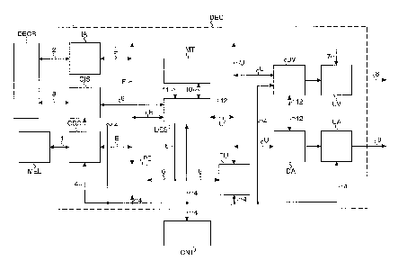
All this said, as can be seen in Figure 1, the device, indicated
overall as DEC, comprises:
a section for connection to sources (or receivers, depending on the
operating mode) of MPEG streams; such section is made up of the
10 following components: CSC, for controlling data transfer on a bus 1
for connection to conventional computer peripheral units; IA, for
connection with a first bi-directional serial line 2 on which data
transfer occurs asynchronously; CIS, for connection with a second bi-
directional serial line 3 on which data transfer occurs synchronously;
15 - a demultiplexing and synchronisation circuit DES, associated to an
external memory MT, intended on one side for temporary storage of
the streams to be demultiplexed and decoded and on the other side
for temporary storage of the demultiplexed audio and video streams
and private data to be sent to the decoders or respectively to the
2 0 controller;
- a section for emitting the audio and video data, comprising the
audio and video decoders DA, DV and circuits to provide users with
decoded data and to mix decoded video signals and graphic signals.
The device also comprises an input bus E and an output bus U
2 5 connected to a bus 4 of external controller CNT. To simplify the
drawing, in busses E, U, 4 the groups of wires intended for data transfer
have not been distinguished from those intended for command and/or
address transfer. Regarding data transfer, the busses are for instance 16-
bit busses. Bus E is used for the exchange of information (data,
3 0 commands...) between IA and CSC on one side and demultiplexing and
synchronisation circuit DES on the other side, for the transfer of private
data included in the MPEG stream from DES to the external controller,
and for the programming of such components and of CIS by external
controller CNT. CIS instead is directly connected to demultiplexing and
3 5 synchronisation circuit DES by means of an additional serial line 6. Bus
U is used for transferring the respective streams to be decoded to audio
and video decoders DA, DV and for programming the decoders
themselves. The two busses E, U are connected to bus 4 by means of
~ 21 66040
s
suitable driving circuits PE, PU, controlled (through signals forwarded
over a connection 5) by circuit DES, so as to avoid conflicts for bus
access by the various components. To simplify the drawing, blocks IA,
CIS, CSC, DES also include the driving circuits which may be necessary
5 to link them with the connections leading to them and the decoding
circuits for the signals which allow CNT to access the different blocks.
Going back to the different blocks making up decoder DEC, unit
CSC is a conventional control unit of a Small Computer System
Interface (SCSI) for reading and writing MPEG data only from and into a
10 peripheral unit (e.g. a local digital storage device MEL) connected to bus
1. Unit CSC is connected both to bus E, for MPEG data transfer, and to
bus 4 of the external controller in order to be programmed by the
controller. For example, unit CSC is realized by means of component
AM53C94 marketed by Advanced Micro Devices. The characteristics and
15 operating modes of such component are not influenced by the present
invention and they are reported in the component data sheets.
Device IA, as previously stated, is to interface decoder DEC with an
asynchronous serial line 2 which can convey data coming from an
MPEG encoder or from a remote memory device, e.g. through a remote
2 0 decoding device DECR identical to DEC. Interface IA is a circuit that
essentially acts as a protocol converter, transforming bi-directional
serial line 2 into a pair of parallel ports, one for signal input and the
other for signal output, connected to input bus E. Interface IA can be
realized, for example, by component C011 manufactured by the firm
2 5 INMOS. The characteristics and operating modes of this component are
not influenced by the present invention and they are reported in the
component data sheets.
Unit CIS is to interface device DEC with a synchronous serial line 3
which, analogously to line 2, allows connection with a remote device
3 0 DECR. Line 3 is to convey data transmitted, for instance, in accordance
with the protocols established by CCITT Recommendations G.703, G.704
with regard to physical layer and frame structure. In this case line 3 is,
for example, a 2 Mbit/s line on which transmission takes place in
accordance with a HDLC (High Layer Data Link Control) protocol,
3 5 overlaid on a PCM frame of thirty-two 64 kbit/s channels. Data
transmitted on line 3 can comprise, in addition to MPEG data, also data
related to fixed pictures, subtitles, texts and graphics and, in general,
data and commands which cannot be inserted in the MPEG streams.
6 2166040
The latter data and commands are exchanged in the form of messages
whose flow is regulated by appropriate control signals provided by DES.
Local decoder DEC and the remote one, DECR, also exchange, through
the same line, the acknowledge signals prescribed by data transfer
5 protocols. Interface CIS can, for instance, be realized by means of
component PCMSC V7311, manufactured by Italtel. The characteristics
and operating modes of this component are not influenced by the
present invention and they are reported in the component data sheets.
When the device acts as a decoder, any one of the aforesaid
10 interfaces can receive data and send them to circuit DES for
demultiplexing. When the device acts as a transmitter of MPEG streams,
the MPEG data are taken through interfaces CSC or IA upon controller's
command and are supplied to interface CIS to be forwarded along line 3
towards device DEC associated to the receiver; through interface CIS, the
15 device can also receive and transmit non-MPEG data, as stated above.
When the device acts as a storage device, it will be able to receive and
transmit data (MPEG or non-MPEG) through CIS: the data received are
forwarded to controller CNT, and the data to be transmitted are
supplied by the same controller.
2 0 Block DES acts as system-layer controller and puts into effect the
different operating modes of the device depending on the programming
provided by the controller.
In particular, in case of decoding, DES must recognise the different
types of signal (audio, video and private data) in the MPEG streams,
2 5 separate them and supply them to the utilisation devices (decoders or
controller) and manage synchronisation; in the course of
demultiplexing, DES also detects errors due to transmission on a noisy
channel and indicates them to the external controller. DES is connected
to external memory MT, which is a Dynamic Random Access Memory
3 0 (DRAM), through a bi-directional data bus 10 and a connection 11 for
memory addressing and control.
For synchronisation, DES exploits information contained in the
MPEG data stream, and in particular the system clock references SCR
which allow local reconstruction of the system clock signal CKS at 90
35 kHz.
When device DEC instead functions as a transmitter or memory
device, DES could even be transparent to the data streams and no
demultiplexing should be effected.
21 66û4Q
Video Decoder DV, which can be programmed by external
controller CNT, receives the compressed video data from DES through
bus U, decodes them with the procedures prescribed by the MPEG
standard and provides the decoded video signals to a video output unit
5 UV, which is to carry out all processing necessary for a picture to be
inserted into a desired display window. UV also includes a built-in
output digital-to-analog converter. If the device is used in association
with a personal computer, block UV also includes components for
overlaying decoded pictures to graphic signals provided by the
10 computer in the form of RGB digital signals through a connection 7.
The analog video signals resulting from decoding are presented on an
output 8. Video decoder DV is conventional and it can be realized for
example by means of component CL450 by C-CUBE. The components of
block UV are also conventional and they can be those carrying out the
15 same functions in association with the above component in the "CL 450
Development Kit" mentioned above.
Audio decoder DA receives, through bus U, the compressed audio
packets to be decoded and carries out decoding operations as prescribed
by the standard. The audio decoder, which can be for instance
2 0 component L64111 by LSI Logic Corporation, provides the decoded
audio signals to an audio output unit UA comprising a digital-to-analog
converter, a processing circuit to perform the signal processing required
by the user and an output amplifier. Audio signals are then provided to
the user through connection 9.
2 5 With reference to Figure 2, demultiplexing circuit DES essentially
comprises: a parser PA, which separates the video and audio streams
and the private data and extracts synchronisation information; a
controller CM of memory MT; a unit DM for managing data transfer
from bus E to the memory and vice versa; devices IS, ICP for interfacing
3 0 circuit DES with synchronous serial line 6 tFigure 1) and controller CNT;
circuits FD for carrying out synchronisation operations; an output
interface IU for interfacing with video and audio decoders.
Parser PA exploits, for its operation, service information contained
in particular fields of the MPEG streams, which fields start with a code
3 5 allowing them to be identified. To make it easier to understand the
functions of PA Figure 3 shows the structure of ISO 11172 layer and of
the audio-visual pack layer, pointing out information of interest to the
invention. Additional details are specified in Part 1 of the standard.
8 2 1 66040
\ -
A transmission arranged in accordance with MPEG standards is
made up of a succession of packs (data or synchronism information)
PACl, PAC2...PACn, each comprising, as indicated for PACl:
- a pack start code PSC,
S - a group of words SCR which code the SCR information;
- a System Header SH, if any, which starts with a System Header Start
Code SHSC and contains service information (INFO) which is valid for
a set of packets. Information contained in this header and of interest
for the operation of PA shall be examined further on;
10 - a certain number of packets PCKl...PCKn: as indicated for PCKl, each
packet starts with a Packet Start Code Prefix PSCP, followed by a
packet header PCKH and then by data PDAT; prefix PSCP contains i.a.
information on packet type (audio/video/private data), while the
header contains the identity of the stream to which the packet refers,
the length of the packet and other information used by the decoders,
in particular time information PTS (Presentation Time Stamp) and
DTS (Decoding Time Stamp).
The last pack, PACn is followed by an end code IEC (ISO 11172 End
Code) .
2 0 The structure and the operation of PA will be described with
reference to Figures 5 -9.
Going back to Figure 2, memory controller CM manages external
memory MT so that the latter is functionally subdivided into four
sections, each arranged in a FIFO structure, intended respectively to
2 5 temporarily store the incoming streams and the demultiplexed audio,
video and private data to be sent to the decoders or to the external
controller. The structure of CM shall be described further on, with
reference to Figures 16, 17.
Unit DM comprises means for managing data exchange between
3 0 memory MT (Figure 1) and units IA and CSC (through bus E) or
controller CNT (through busses E and U). Data exchange is managed in
accordance with the usual Direct Memory Access (DMA) protocols,
which prescribe the emission of a data request signal by one of the
components involved in the exchange and of a signal acknowledging
3 5 data forwarding by the other one. DM is connected to memory
controller CM through a bus M, to which parser PA, serial interface IS
and output interface IU are also connected.
The structure of DM is depicted in more detail in Figures 4 and 10.
~ 9 2166040
Serial interface IS is to extract, from a PCM frame incoming on line
6, information, arranged in accordance with a HDLC protocol, which are
to be processed in PA and, conversely, to arrange in accordance with the
HDLC protocol and insert into a PCM frame, information to be
5 forwarded along line 6 and coming from PA through a connection 16.
The structure of IS will be described more in detail with reference to
Figures 13 - 15.
Output interface IU is to extract, upon request by decoders DA, DV
(Figure 1), audio and video streams from the respective sections of
10 memory MT and to send them to the decoders. In practice, IU consists
of a pair of registers, one for each type of stream, of which the inputs
are connected to bus M and the outputs are connected to bus U. Data
writing and reading occurs upon request by the respective decoders.
Retrieval of the stored signals and their transmission to the decoders are
15 also managed in accordance with DMA protocols.
Interface ICP towards controller CNT (Figure 1) is to manage
addressing by CNT of the internal registers of DES (i.e. the registers
storing information related to programming of DES, supplied by CNT,
and information on the status of DES, made available to CNT) and
2 0 forwarding of interrupt signals (intended for instance to indicate errors,
alarms or data availability) towards CNT, and to arbitrate access to
busses E, U by the different circuits of DES or by controller CNT.
Connection 15 outlines the set of wires for exchanging data and other
signals between ICP and the other components of DES. The structure of
2 5 ICP will be described with reference to Figures 11 and 12.
Block FD comprises the digital part of a phase locked loop (PLL) to
reconstruct system clock CKS starting from indications SCR extracted by
PA and provided through connection 13, and a circuit for generating a
further signal CKESTR, to be provided to PA, which locks the data
3 0 reading frequency from MT to the writing frequency. Note that the
analog part of the phase lock loop (made up of a voltage controlled
oscillator and by a digital-to-analog converter) in reality is external to
device DES, but it was not represented as a separate block to simplify
the drawing. The structure of FD will be described further on, with
3 5 reference to Figures 18 and 19.
The more detailed diagrams which follow do not indicate the
signals related to the protocol for transferring data among the various
components of DES and between these and controller CNT (in general,
2 ~ 66040
request for data sent by a first component to a second, acknowledge by
the latter of the data forwarding and availability of the first component
for a new operation), when such signals are not essential for
comprehension of the invention, as they are altogether conventional; to
S keep the drawing simple, the means for locking the received signals to
the internal timing of each component were also left out; these means,
too, are totally conventional.
Figure 4 is a logic diagram of the data flow through DES. The final
letters E, U of the reference symbols indicate input and respectively
10 output elements in DES. In this Figure, block DM shown in Figure 2 has
been split into the interfaces for connection with blocks IA, CS C, CIS and
with bus 4 in Figure 1, and each of these interfaces is in turn subdivided
into an input section (ITE, ISCE, ISE, IBE respectively for connection with
IA, CSC, CIS and bus 4) and an output section (ITU, ISCU, ISU, IBU). Note
15 that data transfer between DM (Fig. 2) and bus 4 occurs via bus E, as
said, and therefore blocks IBE, IBU are connected to bus E. Moreover in
the diagram the external memory is divided into its four functional
parts BS, BA, BV, BD, the first of which, as stated above, temporarily
stores incoming streams (system buffer) while the others store
2 0 demultiplexed audio and video streams and private data (audio, video
and private data buffers). In an exemplary practical embodiment, the
external memory has a capacity of 64 Kwords (16 bits each) distributed
among the four functional parts in the following manner: BS 16 Kwords;
BA 32 Kwords; BV, BD 8 Kwords each. Where required, reference will be
2 5 made to this example.
Having stated the above, when device DEC is used as an actual
decoder, audio-visual streams coming from any one of the decoder
inputs and conveyed by means of bus E or input part 6E of serial line 6,
enter DES through one of the interfaces ITE, ISCE, IBE or ISE. Only one
3 0 input of DEC, and therefore only one of the input interfaces above, can
provide signals to DES at any given instant: the mutually exclusive
operation is represented schematically by switch SWl inserted between
the interfaces themselves and system buffer BS. The streams to be
decoded, read from BS, are transferred to parser PA which splits the
3 5 streams into the, audio, video and private data components and routes
them towards audio, video and private data buffers BA, BV, BD; video
and audio signals are then forwarded towards their respective decoders
1 1 21 6~0i40
through bus U, while private data are sent towards IBU and from here
to the controller, through bus E.
When device DEC functions as a transmitter, MPEG data provided
by the sources enter through interfaces ISCE, ITE or IBE and after storage
5 they are sent to serial interface ISU; messages (non-MPEG data) to be
forwarded towards IBU can arrive through ISE.
When the device functions as a storage device, MPEG data arrive
through ISE and are forwarded towards IBU. In these two cases,
demultiplexing may or may not be carried out in PA.
The Figure also indicates buffers BME, BMU for temporary storage of
messages received through ISE and respectively of messages to be
transmitted through ISU. It must be stated that, although buffers BME,
BMU are represented as separate blocks, they are actually an integral
part of interface IS, as shall be seen further on.
The different outputs of BS are also activated in a mutually
exclusive way, as shown schematically by switch SW2. Additional switch
SW3 represents the possibility for IBU to receive data either from BS or
from BD.
With reference to Figure 5, in parser PA an incoming data reception
2 0 unit IRD receives from memory controller CM, through bus M, the data
read in BS (Figure 4) and transfers them to the subsequent components
after organising them into a suitable format for these components. The
exchange of data occurs with a conventional protocol entailing a
request to read data by IRD and acknowledge of the dispatch by CM. For
2 5 bus M, too, the Figure does not distinguish the groups of wires carrying
data from those transporting signals related to the protocol or other
commands. Data are requested by IRD to CM with a frequency
determined by signal CKESTR (wires 13a of connection 13 linking PA and
FD, Figure 2), and a reading operation automatically causes the
3 0 memory reading pointer to advance, in a thoroughly conventional
manner. To keep the drawing simple, individual request and
acknowledge signals are not indicated in the drawing. In practice, IRD is
made up of a shift register which carries out a 16-to-8 bit conversion of
the data words read and, on the basis of the information
3 5 communicated by downstream components, supplies them with a new
block of data from which data already used have been eliminated.
Data read from IRD are made available, through a connection 17,
to a unit SD which manages the transfer of data towards serial interface
12 2 1 66040
IS (Figure 2), and, through a connection 18, to four decoding logic
networks D 1 -D4.
Unit SD is to organize the data as required by serial interface IS, in
practice by carrying out an 8-to- 16 bit conversion, and to supply the
5 write and address increment commands for input buffers contained in
IS. Data are present on wires 16a and commands on wires 16b. The two
groups of wires together form connection 16 in Figure 2. Unit SD is
enabled, when necessary, by signals provided by a control unit CPA
through connection 65.
Logic network D 1 is to recognise the codes identifying the fields
allotted to service information concerning system layer and to indicate
to control unit CPA the detection of a code and the type of code
through a connection 60, which includes also the lines conveying
information emitted by logic networks D2 - D4 to CPA.
Logic network D2 is to extract time indications SCR to be made
available to circuits FD (wires 1 3b of connection 13); these indications
are also provided to a parameter memory MP (through a connection 61
which includes also the lines on which the exchange of information
between MP and D3, D4 occurs). Memory MP can also be accessed by the
2 0 external controller (through interface ICP, Figure 2, and wires 15a of
connection 15) which reads the information written by the decoding
logic networks and writes programming data for DES.
Logic network D3 is to extract information contained in the system
header and to send it to parameter memory MP. Information of interest
2 5 for the invention shall be evident from the description of the operation
of PA.
Logic network D4 decodes the packet headers and, on the basis of
the packet header contents and with procedures determined by the
programming information contained in MP, sends, through connections
3 0 62, 63, 64, private data, audio signals and video signals respectively to
units POU, POA, POV. In a preferred embodiment of the invention,
parser PA is able to extract simultaneously the packets related to one of
the streams of private data, one of the audio streams and one of the
video streams multiplexed in the MPEG stream. The identity of these
3 5 streams can be determined by programming information contained in
MP; in the absence of a specific indication, D4 will extract the first
stream identified for each type. In both cases, data from the other
streams will be discarded. Through bus M, units POU, POA, POV then
13 21 66040
supply CM with the signals received from D4 for writing into buffers BD,
BA, BV (Figure 4). This transfer also occurs with the conventional
procedures entailing a write request by the units in PA and acknowledge
of the operation completion by CM.
D4 also extracts, from the packets received, time indications DTS,
PTS already examined above; these indications are utilised with
procedures that depend on the type of audio and video decoders used,
and are also written into parameter memory MP, along with the
identity of the stream to which the packet refers and to the length of
10 the packet.
Logic networks D2 - D4 are enabled in a mutually exclusive way by
CPA by means of signals emitted on a connection 20, and they supply
CPA with information on errors and severe anomalies, which alter or bar
regular operation of the device.
Ports POU, POA, POV are each made up essentially of a register with
8 bit input and 16 bit output and of a logic network for managing the
protocol for signal transfer to the respective sections of memory MT
(Figure 1 ) .
Control unit CPA manages all the circuit operations according to
2 0 the data contained in parameter memory MP (Figure 5), to the
information received from logic networks D 1 -D4 and to possible external
signals, provided by the controller and present on wires of part 4E of
bus 4 coming into DES (Figure 1). Among the external signals, we
mention here a signal START for activating the device operations and a
2 5 signal VIDEO_AUDION which, along with information contained in MP,
disables decoding of the audio and video packets when these operations
are to be carried out in other circuits. For this purpose the inputs of
POA, POV are connected to the outputs of respective multiplexers MX3,
MX4 which are controlled by ~PA through a signal present on a
3 0 connection 66 and which have a second input connected to an
additional output connection 21 of IRD, on which the packets are
present. The two multiplexers are operated in a mutually exclusive way,
as indicated by inverter INV.
CPA signals errors or anomalous situations to interface ICP (Figure
3 5 2) in the form of interrupt requests emitted on wires 15b of connection
15.
The operation of device PA shall now be described, referring also to
the flow charts in Figures 6 - 9.
1 4 2 1 6~4a
As can be seen in Figure 6, after receiving the START signal, the
parser control unit CPA (Figure S) must first check whether signal
VIDEO_AUDION indicates that parsing is or is not to be effected. In the
latter case, as stated above, CPA positions multiplexers MX3, MX4 on the
5 input linked to connection 21 so that the packets are transferred
directly from IRD to output ports POA, POV. If parsing is to be effected,
CPA positions the multiplexers on the inputs connected to the outputs
of D4, enables logic network Dl and starts waiting for a code (SEARCH
CODES). Under regular operating conditions, D 1 should detect first a
10 pack start code, then a possible system header start code and then the
packet start codes. As long as the pack start code is not arrived, all bits
arrived to circuit DES are discarded. Upon the arrival of each code (step
100), Dl decodes it and CPA will follow three different paths depending
on the code received. The three paths are indicated synthetically in
Figure 6 by steps 101 (parse pack header), 102 (parse system header),
103 (parse packet). Each of these three paths corresponds respectively
with the enabling of one of the logic networks D2 - D4, as indicated by
steps 104, 105, 106 in Figure 7. Note that step "SET SEARCH FLAG" in Fig.
7 corresponds to step "SEARCH CODES" in Fig. 6.
2 0 If the code is the pack start code, logic network D2 (Figure 5) parses
the pack header (step 101), extracting system clock references SCR and
providing them to block FD (Figure 2) for reconstruction of signal CKS.
When a system header start code is recognized, the operations of
step 102, illustrated in greater detail in Figure 8, are carried out. Logic
2 5 network D3 (Figure S) must decode certain parameters contained in the
header and supply them to parameter memory MP. The meaning of
these parameters, which are indicated in the flow chart in Figure 8, is
known from the standard. CPA carries out checks on the values of some
of these parameters - in particular those related to the stream rate
3 0 (RATE_BOUND) and to the minimum memory size required by private
data (STD_BUFFER_SIZE_BOUND), and a pair of flags F and CSPS
indicating characteristics of the flow (transmission at fixed rate and
bound parameters) - to verify whether the values themselves are
acceptable (stream rate and memory capacity) or are the desired ones
3 5 (for the two flags). If the outcome is negative, a signal that decoding is
impossible is generated and presented on one of the wires 15b. Under
these conditions, the parser operations are blocked until the arrival of a
new START.
2 1 66040
If the code received is a packet start code, the operations of step
103, shown in greater detail in Figure 9, are carried out. CPA enables D4
to decode information contained in the packet header, in particular the
identity of the stream to which the packet belongs, to verify whether
5 the stream is actually the one being processed. If the header indicates
that the packet is a video packet belonging to the current stream, the
length of the packet is stored in MP; the presence of signals DTS (if any)
is indicated to the external controller and, after the controller reads
these signals, the transfer towards POV of the data contained in the
10 packet is commanded for the subsequent forwarding to video buffer BV
(Figure 4) and then to video decoder DV (Figure 1).
If the packet is not a video packet, CPA examines whether it is an
audio packet or a private data packet. If it is an audio packet belonging
to the desired stream, its length is stored in MP, the signals PTS which
15 may be present are read and the transfer of the data contained in the
packet towards POA for storage in BA is commanded. If it is a private
data packet, the forwarding of the data contained in the packet
towards POU for storage in BD is commanded.
When PA eventually receives the end code, it goes back to rest.
2 0 It should be stated that, regarding video signals and private data,
only "net" data are transferred to the output, that is data without the
service information contained in the header, as prescribed by the
standard. For audio, it is possible both to transfer net data, as
prescribed by standard ISO/IEC 11172-3, and to transfer the whole
2 5 packet, depending on the characteristics of the audio decoder.
Figure 10 shows the block diagram of DM. Elements also illustrated
in Figure 4 are indicated with the same references. DM comprises an
input section (blocks ITE, ISCE, IBE) which transfers data coming from
IA, CSC and CNT (Figure 1) on a connection EE to memory controller
3 0 CM, through a multiplexer MXl and a connection or bus MW,
representing that part of bus M which conveys signals directed to
memory controller CM (Figure 4), and an output section (blocks ITU,
ISCU, IBU) which routes to IA, CSC and CNT, through a multiplexer MX2
and a connection EU, signals read in BS and present on a connection or
3 5 bus MR, representing that part of bus M (Figure 2) destined to convey
signals outgoing from CM. Connections EE, EU and MW, MR are uni-
directional connections obtained by separating, in a thoroughly
2166040
16
conventional way, the two directions of transmission of busses E and
respectively M at the input into DM.
If the device of the present invention is placed on the decoding
side of a transmission system for MPEG streams, circuit ITE receives 8-bit
5 data blocks from IA and arranges them into 1 6-bit blocks to be
transferred to controller CM and to BS. Circuit ITU receives from
controller CM, through an appropriate wire of bus MR, information on
the filling level of memory BS (signal STAT which shall be examined in
the course of a detailed description of CM) and sends towards IA,
10 through a wire of EU, a request to discontinue data transmission, if the
filling level of BS has exceeded an upper threshold, or a request to
resume transmission, if the filling level of BS has dropped below a lower
threshold. Both thresholds are programmable.
If the device is used on the transmitter side, ITU will split the 16-
15 bit blocks of data read in the memory into two bytes and will sendthe~n sequentially to IA; ITE receives from IA and sends to CM feedback
signals coming from the receiver.
ITE, ITU are each realized by means of two finite-state machines,
one dedicated to receiving data from outside and forwarding them to
2 0 the memory, and the other one to managing control signals. Since the
dialogue protocol is standard, the expert in the field has no problem in
realising these devices.
Circuits ISCE, ISCU, IBE, IBU comprise a pair of registers in a ping-
pong arrangement (i.e. a pair of registers alternating at each cycle in
2 5 the reading and writing operations) and a logic network for managing
request/acknowledge signals prescribed by the protocol. Data coming in
or going out through these circuits in the different modes of operation
are clearly shown by what has been described above.
Through wires l5c of connection 15, all circuits in DM also receive
3 0 from ICP (Figure 2) command STOPE to stop respective operations when
controller CNT (Figure 1) requests access to bus E, and they send to ICP,
through wires 15d, which also belong to connection 15, a signal STOPDE
to acknowledge that the stop has occurred.
With reference to Figure 11, block ICP comprises three logic
3 5 networks GIR, CDE, CAC which respectively are to manage the interrupt
requests, to decode the addresses of the internal registers in DES and to
arbitrate access requests to busses E, U (Figure 1) coming from DM, IU
(Figure 2) or controller CNT.
- 216604Q
17
GIR receives interrupt requests from PA, CM and IS through wires
15b of connection 15, each wire being associated with a specific request
IRQX. It is assumed, by way of example, that 16 distinct requests can
reach GIR. In the presence of such requests, GIR sends a flag IRQ to
5 controller CNT (Figure 1 ) through a wire of bus 4U (which represents the
part of bus 4 that egresses from DES) and subsequently, when receiving
command RIRQ from CNT through bus 4E, it makes available the
requests on bus EU. GIR also comprises means to prevent requests
arriving while a previous request is being processed, from being erased
10 without having been served. The structure of GIR shall be described with
reference to Figure 12.
Circuit CDE managing register addressing accomplishes an indirect
addressing, which entails, in an initial operation, dispatching the
address to CDE and, in a second operation, actually writing/reading the
15 data into/from the register. CDE essentially consists of a decoder which
receives the address through bus EE and presents, on wires 15e of
connection 15, the enabling signals for the individual registers. Indirect
addressing is a well known technique for the skilled in the art and
therefore circuit CDE does not require a more detailed description.
2 0 Circuit CAC manages access to busses E, U so that these busses are
normally assigned to DM or respectively to IU and are assigned instead
to controller CNT (Figure 1 ) when the latter requests so. The circuit
comprises two identical elements, each of which manages access to one
of the two busses. The access request by the controller is signal IOBUS
2 5 which is presented by CNT on one of the wires of bus 4E and indicates,
depending on its logic value, whether access to bus E or to bus U is
involved. As a consequence of the request, CAC generates, depending on
the element concerned, the signal STOPE (wires 15c) or STOPU (wires
15f) requesting operations of circuits DM or IU to stop; after receiving
3 0 acknowledge signals STOPDE, STOPDU, provided by the components
involved through wires 15d, 15g and indicating that the stop has
occurred, CAC will generate enabling signals OEE, OEU for the driving
circuits PE, PU on wires SE, 5U, which form connection 5 in Figures 1, 2;
CAC will also receive the usual reading/writing (R/W) and chip select
3 5 (CS) commands and it will send the availability signal RDY to the
controller. A circuit of this kind is totally conventional.
Further input/output signals into/from ICP will result from the
description of other blocks of DES (Fig. 1).
21 66040
- 1 8
With reference to Figure 12, in the example considered here of 16
possible interrupt requests, circuit GIR comprises a bank of 16 latch
registers Ll. Each element has its gate input connected to one of wires
1 Sb and, upon receipt of request IRQX, it transfers at the output a signal
5 at pre-set logic level (in particular 1). The outputs of the different
elements of Ll are connected to the inputs of an OR gate, indicated as
Pl, whose output is the wire of bus 4U conveying flag IRQ, signalling the
presence of an interrupt request, to controller CNT. Moreover, the
outputs of Ll are each connected to one of the registers of a bank of 16
10 registers Rl, which store interrupt requests and transfer them on bus EU
(signal IRQR) upon reception of a reading command RIRQ supplied by
the controller through a wire of bus 4E. Each output signal of Rl is also
fed back to the reset input of the respective element in L 1 through the
series of an AND gate and a NOR gate, belonging to respective gate banks
15 P2, P3. Each gate in P2 is enabled by a pulse which is derived by a pulse
generator GIM from the reading command for the respective register in
R 1. In practice, GIM can be a differentiating circuit. The individual
gates in P3 are enabled by a respective output signal of a bank of 16
enabling registers R2 which, upon command of a writing signal provided
2 0 by CDE (Figure 11) through one of the wires 15e, load a signal which
enables processing of individual interrupt requests and which is
supplied by the controller through bus EE. It is evident that, with the
arrangement described here, an interrupt request is not reset and it is
kept available to the controller until it is actually read by the latter. In
2 5 this way, requests arriving while the controller is already processing
another request are not lost. Moreover, through register R2 and ports P3
it is possible to mask interrupts individually.
Figure 13 shows that interface IS towards serial line 6 comprises a
transmit section STX and a receive section SRX, which correspond to the
3 0 set of blocks BMU, ISU and respectively ISE, BME in Figure 4. If device
DEC (Figure 1) is utilised as a transmitter, transmit section STX is
essentially to forward MPEG data and messages, while receive section
SRX receives and makes available to the controller the signals
acknowledging message reception, coming from the device associated to
3 5 a remote decoder; vice versa, in device DEC associated to the receiver,
section STX transmits the acknowledge signals provided by the
controller and the receive section receives data and messages, sends the
~ 1 9 2 1 66~`4Q
former to the system buffer and makes the latter available to the
controller.
The transmit section has to arrange transmission of signals in
HDLC protocol within a PCM frame, by taking into account on one hand
5 the protocol characteristics and on the other the fact that certain
channels of a PCM frame are reserved to synchronism information and
to signalling and cannot be used for communications. The HDLC
protocol used in the present application uses "frames" including, in
order:
10 - at least one initial synchronism word, characterized by six
consecutive " 1 " bits; synchronism words can be multiple if this is
required to adapt the channel filling to the bit rate actually required;
- an "address" word, comprising a group of bits specifying the type of
information transmitted, namely MPEG data, message or acknowledge
15 signal; in this last case, the address word also encodes the meaning of
the acknowledge signal itself;
- a succession of words representing the transmission information
content (these are obviously missing in case of transmission of an
acknowledge signal);
2 0 - two words for checking the transmission correctness (in particular,
two words representing a cyclical redundancy code).
Further detail on the frame structure indicated can be found in
international standard ISO/IEC 3309.
Having taken that into account, transmit section STX comprises:
2 5 - a data generator GD, comprising two elements which store
respectively data coming, for instance, from unit SD (Figure 5) of
parser PA through connection 16 and messages provided by the
controller through bus E; GD forwards the data/messages, one byte at
a time, to a HDLC frame forming device TH, when GD receives the
3 0 corresponding request from TH; the memory element for the messages
is block BMU in Figure 4.
- HDLC frame forming device TH, which inserts the synchronism words
and the address at the start of the frame, breaks up sequences of 1 ' s
which, in the information words, could simulate the synchronism
3 5 word (in particular, by inserting a O after five consecutive l's), and
computes the cyclical redundancy code, adding it at the end of the
frame; the structure of TH shall be described further on, with
reference to Figure 14;
~ 20 2t 66040
- an output interface IPT, which requests from TH, one bit at a time,
the signals to be transmitted and inserts them into a PCM frame on
the basis of the synchronism information provided by CIS (Figure 1)
through line 6E; the PCM frame is then emitted on connection 6U.
The receive section is complementary to the transmit section
and comprises:
- an input interface IPR which extracts, one bit at a time, HDLC data
from a PCM frame present on line 6E, on the basis of synchronism
information supplied by CIS through the same line 6E;
10 - a device RH for splitting the HDLC frame, whose tasks are
complementary to those of TH and which has to recognise the type of
information transmitted, transferring MPEG data and messages, one
byte at a time, to a data receiver RXD, and making available the
acknowledge signals to controller CNT (Figure l); the structure of RH
is illustrated in detail in Figure 15;
- data receiver RXD, which stores in data or message buffers the bytes
received from RH before forwarding them respectively to BS (Figure 4)
and CNT (Figure 1) through busses MW, EU; the data buffer is
composed of two elements in a ping-pong arrangement and it is to
2 0 store data for the time needed by the memory controller to obtain
access to BS; the message buffer (which has been indicated as BME in
Figure 4) on the contrary is a FIFO memory, storing complete
messages and signalling that it has been filled (and therefore that
messages are present), by an interrupt request.
2 5 With reference to Figure 14, in block TH a multiplexer MX5 has four
inputs connected respectively: to connection 22 over which GD (Fig. 13)
presents information to be transmitted; to means supplying the
synchronism word (arrow FL), obtained through the appropriate group
of wired logic levels; to output 70 of a circuit CRT computing the
3 0 cyclical redundancy code in transmission; to output 71 of a circuit SIH
for selecting the HDLC address. MX5 is positioned on the appropriate
input, depending on the phase of the transmission, by a command
emitted on a connection 27 by a control logic network LCT, which also
requests the data bytes from generator GD, through a signal UNBYTE
3 5 emitted on wire 23.
Circuit SIH comprises three registers into which the controller
writes, through bus EE, the values assigned to the address word
respectively for data, messages and acknowledge signals. Through
2 1 66040
21
connection 71, SIH provides MX5, on the basis of a control signal
emitted by LCT on a connection 28, with word ADDR corresponding to
the type of information transmitted. SIH also makes available the
values utilised to block RH in Figure 13 (signal DAM present on a
5 connection 25), so that the latter can correctly interpret the
information received. Obviously, such values shall also be notified to
remote device DECR (Figure 1), if present.
Output 72 of multiplexer MX5 is connected to a parallel-to-serial
converter PS, whose output 29 (signal OUTS) is connected both to CRT
1 0 and to a device UNT which emits the data on serial output 24 after
breaking up the sequences of consecutive 1 ' s as stated above. Circuit PS
loads the bytes coming out of MX5 upon command of logic network LCT
(LOAD, wire 30), to which PS signals (wire 30a) that a byte has been
forwarded to UNT. The break-up of sequences of l's is disabled by LCT
1 5 (signal DISUNI present on a wire 31) when the bit string on wire 29 is
related to a synchronism word. UNT also receives from IPT (Figure 13)
the bit request (signal UNBIT) through wire 26 and transfers it, through
a wire 32, both to PS, as a shift command to cause the presentation in
output of a new bit, and to CRT as a command to load the bit coming
2 0 out of PS so that the bit can be taken into account in the redundancy
code computation. The realization of a circuit performing the functions
of UNT is not a problem for the skilled in the art.
With reference to Figure 15, in circuit RH for splitting the HDLC
frames, a block UNR, whose tasks are complementary to those of block
2 5 UNT (Figure 14), receives from IPR (Figure 13) the serial stream of signals
present on a wire 33, discards the 0's which UNT may have inserted,
and recognises and signals to a control logic network LCR, through a
wire 37, the arrival of a synchronism word (signal FLG). Data output 38
of UNR (signals OUTU) is connected to a serial-to-parallel converter SP
3 0 and to a circuit CRR for checking the cyclical redundancy code, which
circuit signals to LCR that the two words related to that code have been
recognized (signal CRCOK on wire 39, which is also stored in a register of
LCR to be made available to the controller, e.g. through ICP, Figure 2, as
represented schematically by wires lSi). Output 40 of SP (signals POUT)
3 5 is connected to a circuit VIH for checking the HDLC address and to an
output buffer memory PIP, with a capacity of two words, which makes
available the words emitted by SP to data receiver RXD after storing
them for a time interval equal to the duration of two words. Storing the
22 2 1 66Q40
~,
two words is aimed at preventing the words related to the cyclical
redundancy code from being sent to downstream components, as the
following description will clarify. Circuit VIH is enabled by LCR to load
the address, after RH has received the synchronisation word or words,
5 through command WRADDR on wire 41, and to compare such address
with signal DAM supplied by the transmitter, to recognise the type of
transmission. Information on the type of transmission is communicated
to LCR (signal AD on connection 42) which, in case of data or messages,
must have the information contents of the transmission loaded into the
10 appropriate memory of RXD (Figure 13) through data write commands
WD or message write commands WM generated on wires 35, 36. The
emission of such commands is inhibited in the presence of synchronism
words, of the address or of the cyclical redundancy code. If the
transmission concerns an acknowledge signal, VIH makes it available to
15 the controller through ICP (signal ACKDAT present on wires 1 Sh) . LCR
also emits, on the appropriate wire 15b, the interrupt request ACKREC.
To keep the drawing simple, the reading request signals for ACKDAT and
CRCOK are not shown.
The operation of RH is as follows. The arrival of a synchronism
2 0 word after a series of different words indicates to LCR the start of a
HDLC frame: this means that the two words which at that moment are
stored in PIP are the words of the cyclical redundancy code of the
preceding frame, which must not be forwarded to downstream
components, so that LCR does not emit signals WD, WM. After the first
2 5 synchronism word, RH can receive other synchronism words or the
HDLC address: if other synchronism words arrive, these are signalled by
an equal number of signals FLG to LCR; when, in correspondence with a
new word, signal FLG is no longer present, LCR issues the address loading
command WRADDR: in these cases, too, the write commands are not
3 0 generated. They shall be generated only after receipt of the address,
with a delay of two byte times, so that the first information word is
- actually present at the output of PIP.
Figure 16 shows the block diagram of memory controller CM.
Controller CM has to process either access requests by the components
3 5 of DES (Figure 1) to one of sections BS, BA, BV or BD (Figure 4) for
writing/reading MPEG streams to be demultiplexed or demultiplexed
streams, or access requests by controller CNT (Figure 1) to any memory
position. In the example shown, it is assumed that CM can therefore
23 2 1 66040
receive five distinct writing requests and five distinct reading requests:
four of the reading/writing requests come from components of DES and
regard only one section among BS, BA, BV or BD (in particular ISCE, ITE,
ISE, IBE, Figure 4, can write into BS; ISCU, ITU, ISU, IBU can read from BS;
5 PA can read from BS and write into BA, BV, BD; IU can read from BA, BV);
the other reading/writing request is the one supplied by CNT and, for
the purposes of this request memory MT (Figure 1) is seen as a single
unit. A different pointer shall correspond to each of the five
reading/writing requests: pointers for operations required by
10 components of DES select the address in the group corresponding to the
particular section and will allow a FIFO management of the sections; the
pointer for access by CNT instead points to the address communicated
by CNT.
This said, block CM comprises:
15 - an arbitrating circuit ARB which receives the memory writing/reading
requests and selects the corresponding pointer (signal ADPU and
write/read signals WR/RD). Note that requests coming from DES
(Figure 2) arrive through MW and those coming from the controller
arrive through wires of connection 15: for the sake of simplicity, no
2 0 distinction is made between the different request sources and the
requests are indicated overall as REQW, REQR respectively for writing
and reading. ARB also checks the filling condition of the individual
sections, generating a certain number of signals about that condition,
which will be examined in connection with Figure 17, which provides
2 5 a detailed illustration of the structure of ARB. Some of these signals,
indicated overall as STA, are utilised outside ARB;
- a circuit CIM which controls memory addressing and which, on the
basis of the information supplied by ARB, identifies the section
involved and generates on connection 11 the read or write command
3 0 (MEMCONTR) and the addresses (MEMADDR) with the procedures
required by the protocols for managing a Dynamic RAM memory;
these procedures are thoroughly conventional and therefore it is not
necessary to describe CIM in detail;
- a pair of registers RER, REW for temporary storage of data read from
3 5 the memory (which arrive through connection 10R, belonging to
connection 10 in Figure 2, and which must be transferred on MR) or
respectively of data to be written into the memory (which arrive
through MW and must be transferred on connection 10W, also part of
21 66040
~_ 24
connection 10 in Figure 2); the data are loaded into RER, REW upon a
command from CIM (wires 44, 45).
At the end of each operation, CIM supplies ARB with an operation
end signal RDY (wire 48) and ARB in turn will be able to send to the
5 requesting component acknowledge signals ACKR, ACKW that reading or
writing has occurred, through the wires of bus MR or of connection 15
(request by DES or respectively by CNT, Figure 1). In this case too, no
distinction is made between acknowledge signals directed to DES or to
the controller.
With reference to Figure 17, circuit ARB comprises:
- - a ten-input multiplexer MX6, which receives the ten possible requests
REQW, REQR for access to the memory and forwards a request at a
time on an output 50, upon command of a counter CNl;
- a circuit GPU to generate the ten read/write pointers;
15 - a circuit DAK to generate acknowledge signals ACKR, ACKW;
- a control logic network LCA.
Counter CNl is a counter that normally carries out a cyclical count
to command sequentially the connection of the ten inputs of MX6 to
output 50, thereby allowing sequential processing of the access requests,
2 0 e.g. following the technique commonly known as round robin.
Conveniently, the inputs of MX6 are arranged in such a way that there
is an association between reading/writing requests and even/odd count
values of CNl: e.g. even values can select the inputs carrying reading
requests REQR and the odd ones can select the inputs carrying writing
2 5 requests REQW. CNl can however also be programmed by the controller
in such a way as to connect only pre-set inputs of MX6 to the output.
Request REQ transferred tO the output of MX6 is supplied both to
control logic network LCA for being processed and to CNl as a command
for temporarily stopping (signal STOP) the sequential count, which will
3 0 be resumed upon command from LCA (signal RESTART) once the request
has been served.
The count value present on output 51 of CNl is also supplied to
pointer generating circuit GPU, to control logic network LCA and to
acknowledge generating circuit DAK.
3 5 Circuit GPU, on the basis of the value present on connection 51
and of the address supplied by CNT (Figure 1) through bus EE (in case of
request coming from CNT), sends signal ADPU to CIM (Figure 16) to
address the pointer involved. The writing address issued by GPU is
21 6604~
always the address of the first free position, while the reading address is
always that of the first occupied position. After each operation, GPU
increases the pointer upon command of a signal INC supplied by LCA.
Clearly, in case of operation requested by CNT, increasing a pointer has
5 no effect if the previously carried out operation involved only one cell
and CNT has, in the meantime, loaded a new address into GPU through
EE. The procedures for handling memory pointers, described above, are
well known in the art.
GPU also carries out a comparison between the reading pointer and
10 the writing pointer to measure how full the memory is and generates
three signals indicating the result of the comparison. A first signal is
signal STAT which indicates whether the filling level is between a lower
and an upper threshold or whether it has exceeded the upper threshold
as an effect of a writing operation or it has dropped below the lower
15 threshold as a result of a reading operation: as has been stated above,
this signal is supplied to block ITU (Figure 19) to generate the requests
for suspension or resumption of data dispatching; the threshold values
are programmable and they are supplied to GPU by controller CNT,
through bus EE. A second signal (ISTAT) indicates instead the condition
2 0 of full or empty memory and it is supplied to control logic network LCA
which, on the basis of the value of this signal and of the type of
operation requested (which, with the hypothesis made on the count
values of CNl, is signalled by the least significant bit of the value
present on connection 51 ), decides whether to perform the operation,
2 5 and therefore to generate the respective command towards CIM and
then to send the acknowledge that the operation has taken place, or to
send an interrupt request FVP towards ICP (Figure 2). A third signal
(LEVEL) represents the difference between reading and writing pointers
in the system buffer and it is supplied, again through wires of bus MR,
3 0 to FD (Figure 2) which uses it to generate signal CKESTR: signal LEVEL
can be a 4 bit signal, which, in the example considered, in which B S
(Figure 4) has a 16 bytes capacity, corresponds to ex~mining the filling
level of the memory in 1 byte steps. Signals STATS and LEVEL are the
signals indicated as a whole by STA in Fig. 16. The various signals
3 5 generated by GPU are also kept available to controller CNT, which can
request them to be presented on bus EU. Realising a circuit carrying out
the functions described above presents no problem to the skilled in the
art .
26 21 66040
Acknowledge signal generating circuit DAK is a simple decoder
which receives a signal ACK acknowledging the completion of an
operation by LCA and, depending on the value present on connection
51, generates one of five possible write acknowledge signals ACKW, or
5 five read acknowledge signals ACKR. The signal generated is sent to the
component which requested the operation in the memory.
Control logic network LCA is a conventional finite state machine,
whose operations are inferred from the description above. For the sake
of clarity, such operations are summarised here: LCA, receiving a signal
10 REQ and the count value of CN 1 , which specifies whether the request
concerns a writing/reading in the system, audio, video or user buffers, or
a writing/reading requested by CNT and therefore regarding the memory
as a whole, checks the memory condition tO see whether the operation
can be performed: in the negative, LCA emits the interrupt signal FVP on
15 a wire 15b and, in the affirmative, it generates the writing/reading
command WR/RD on wire 47, emits the acknowledge signal ACK and the
pointer increment signal INC and, at the end of the acknowledge signal,
send signal RESTART to CNl. Designing a logic network carrying out
these of operations is not a problem for the skilled in the art.
2 0 Figure 18 shows that the circuit generating CKS comprises:
- a register REl which loads the value of time stamp SCR taken from
the MPEG pack and supplied by PA (Figure 2) through wires 13b of
connection 13;
- a subtractor STl, which carries out the subtraction between the value
of SCR received from REl and a local value SCR' of SCR, supplied by a
counter CN2 controlled by signal CKS, and generates an error signal
el;
- a digital filter Fl, which performs low-pass filtering of the error signal
e l; filter Fl is a filter of which the zeroes, the poles and the gain can
3 0 be programmed by the controller via interface ICP (Fig. 2); connection
l5j schematizes the link between Fl and ICP necessary for the
addressing, the loading of the programmed values, the exchange of
dialogue protocol signals;
- a digital-to-analog converter DAC, which receives the filtered error
3 5 signal and converts it into analog form to regulate the frequency of a
voltage-controlled oscillator VCO, of which the output 12 conveys
reconstructed signal CKS at 90 kHz.
~ 27 2 1 66040
Note that, for a correct circuit operation, filter F 1 shall be
initialised so that the first local value SCR' of SCR corresponds to the
value loaded in REl.
With reference to Figure 19, the circuit for generating CKESTR
5 comprises:
- a subtractor ST2, which receives from the memory controller, through
bus MR, the signal LEVEL representing the difference between reading
and writing pointers and introduces on that difference a fixed offset
OFF, for instance such that the equilibrium condition, which does not
require a correction of the CKESTR frequency, corresponds to the
situation of half-full memory: in the example considered, in which
the filling level is evaluated in a sixteen-value scale, OFF will have
value 8;
- a sampling register RE2, which samples the output signal of ST2,
representing an error signal e2, with frequency fc (e.g. 8 kHz or 1 kHz)
much lower than the frequency of variation of the signal LEVEL; the
command for loading signal e2 into RE2 is supplied by the decoder
time base (not represented);
- a digital filter F2, which carries out a low-pass filtering of signal e2;
2 0 also F2 is programmable by the controller, exactly alike Fl (Fig. 18);
connection 15k, having the same purposes as connection 15j
schematizes the link between F2 and ICP (Fig. 2);
- a divider DIV, which divides a fixed-frequency signal (in particular a
23 MHz signal) fe, generated by the time base of decoder DEC~, by the
2 5 signal coming out of filter F2 and generates signal CKESTR, which is
sent to PA through wires 13a of connection 13.
Note that it is also possible to program the above described circuit
so as to utilise a fixed value of CKESTR, obtained by setting a fixed
division factor in DIV.
3 0 It is evident that what has been described is given solely by way of
non-limiting example, and that variations and modifications are
possible without departing from the scope of the invention.