Note : Les descriptions sont présentées dans la langue officielle dans laquelle elles ont été soumises.
CA 02166504 1999-08-11
-1-
MULTILAYER PILLAR STRUCTURE FOR IMPROVED
FIELD EMISSION DEVICES
Field of the Invention
This invention pertains to field emission devices and, in particular, field
emission devices, such as flat panel displays, having an improved pillar
structure using a
mufti-layer material co~guration.
Background of the Invention
Field emission of electrons into vacuum from suitable cathode materials is
currently the most promising source of electrons in vacuum devices. These
devices include
flat panel displays, klystrons and travelling wave tubes used in microwave
power
amplifiers, ion guns, electron beam lithography, high energy accelerators,
free electron
lasers, and electron microscopes and microprobes. The most promising
application is the
use of field emitters in thin matrix-addressed flat panel displays. See, for
example, J. A.
Costellano, Handbook of Display Technology. Academic Press, New York, pp. 254
(1992).
1 S Diamond is a desirable material for field emitters because of its low-
voltage emission
characteristics and robust mechanical and chemical properties.
A typical field emission device comprises a cathode including a plurality of
field emitter tips and an anode spaced from the cathode. A voltage applied
between the
anode and cathode induces the emission of electrons towards the anode.
A conventional electron field emission flat panel display comprises a flat
vacuum cell having a matrix array of microscopic field emitters formed on a
cathode of the
cell (the back plate) and a phosphor coated anode on a transparent front
plate. Between
cathode and anode is a conductive element called a grid or gate. The cathodes
and gates are
typically skewed strips (usually perpendicular) whose intersections define
pixels for the
display. A given pixel is activated by applying voltage between the cathode
conductor strip
and the gate conductor. A more positive voltage is applied to the anode in
order to impart a
relatively high energy (400-3,000 eV) to the emitted electrons.
The anode layer is mechanically supported and electrically separated from
the cathode by pillars placed sparsely so as not to drastically reduce the
field emission
areas of the display. In order to withstand the high voltage applied to the
anode for phosphor
excitation, the pillar material should be dielectric and should
~16G~0~
-2-
have high breakdown voltage.
One of the limiting factors in the display performance in the flat panel,
field emission display (FED) is the allowable maximum operating voltage
between
the cathode emitter and the anode. The measured efficiency for typical ZnS-
based
phosphor, (e.g. the P22 red, green, and blue, as commercially available from
GTE)
increases approximately as the square-root of the voltage over a wide voltage
range,
so a field emission display should be operated at as high a voltage as
possible to get
maximum efficiency. This is especially important for portable, battery-
operated
devices in which low power consumption is desirable. The applicants have also
found that the electron dose that phosphors can survive without substantial
degradation of their luminous output similarly increases with operating
voltage. It is
not generally recognized that the combination of these two effects makes it
especially advantageous to operate at high voltage. The display needs to
produce the
same light output, irrespective of its operating voltage. Since the efficiency
improves at high voltage, less total power must be deposited on the anode.
Further,
since the power is the anode voltage times the current, the current required
to
maintain a constant light output decreases even faster than the power. When
this is
combined with the above-mentioned increase in dose required to damage the
phosphor, the lifetime is found to be a strongly increasing function of the
voltage.
For a typical phosphor, we anticipate that changing the operating voltage from
SOOV
to SOOOV would increase the device's operating lifetime by a factor of 100.
Most practical field emission displays require integrated dielectric
pillars to keep the substrate and screen separated. Without these pillars, the
pressure
difference between a normal atmosphere outside and vacuum inside will flex the
anode and the cathode surfaces together. Because of the insulator breakdown in
high
electrical fields, these pillars put limitations on the voltage that can be
applied to the
display, and consequently limit the phosphor efficiency and thus the power
consumption. The voltage limitation arises because it is necessary to avoid
electric
discharges along the surface of the pillars.
There is a substantial amount of knowledge on surface breakdown on
insulators in vacuum, see a review paper by R. Hawley, Vacuum, vol. 18, p. 383
( 1968). For insulator surfaces oriented parallel to the electric field,
typical electric
fields at which breakdown occurs seem to be no better than 104 V/cm (e.g.,
5000 V
across a 5 mm length). This is dramatically lower than the 1-10 x 106 V/cm
that
most solid insulators will support through the bulk. Smaller dielectric
objects will
support larger electric fields, for example, 200 p.m high pillars will
typically support
.
-3-
about
2-5 x 10⁴ V/cm, but the overall voltage (which is field times height) is still
a
monotonic function of height.
Since field emission displays with ZnS-based phosphors are desirably
operated at 2000V or more (even more desirably at 4000V or more), a straight-
walled pillar would have to be O.Smm - lmm tall (allowing for a safety factor
of
1.5). Such tall pillars lead to difficulties in keeping the electrons focussed
as they
travel between emitter and the phosphor screen.
The applicants are not aware of any literature that discusses the effects
of electron bombardment on dielectric breakdown, but it seems likely that it
will
decrease the breakdown voltages further, and thus require yet taller pillars.
If we consider an insulating surface in a vacuum containing a few
electrons, the insulator surface will generally become charged. The sign of
the
charge is not necessarily negative. Incoming electrons can knock electrons off
the
insulator, a process known as secondary emission. If, on average, there is
more than
one outgoing electron per incoming electron, the insulator will actually
charge
positively. The positive charge can then attract more electrons. This process
doesn't
run away on an isolated block of insulator, because the positive charge
eventually
prevents the secondary electrons from leaving, and the system reaches
equilibrium.
However, if we put the insulator between two electrodes and establish a
continuous voltage gradient across the insulator, the secondary electrons can
always
hop toward the more positive electrode. One can get a runaway process where
most
of the insulator becomes positively charged (to a potential near that of the
most
positive electrode) so that the voltage gradients near the negative electrode
becomes
very strong. These stronger gradients can lead to field emission from the
negative
electrode, and another cycle of charging and emission. This process can lead
to the
formation of an arc across the surface long before the insulator would break
down
through the bulk. Accordingly there is a need for novel and convenient methods
for
producing and assembling a pillar structure with desirable geometrical
configurations and dielectric properties.
Summary of the Invention
A field emission device is provided with an improved pillar structure
comprising mufti-layer pillars. The pillars have a geometric structure that
traps most
secondary electrons and an exposed surface that reduces the number of
secondary
electrons. Processing and assembly methods permit low-cost manufacturing of
high
CA 02166504 1999-08-11
-4-
breakdown-voltage devices, including flat panel displays.
In accordance with one aspect of the present invention there is provided in a
field emission device comprising an emitter cathode, an anode and a plurality
of insulating
pillars separating said cathode and anode, the improvement wherein: at least
one of said
plurality of insulating pillars comprises a multilayer structure composed of
alternating
conducting layers and insulating layers; wherein said insulating layers are
recessed with
respect to said conducting layers to form grooves in said at least one of said
plurality of
insulating pillars.
In accordance with another aspect of the present invention there is provided a
method for making a field emission device comprising an emitter cathode
electrode, an
anode electrode and a plurality of insulating pillars separating said
electrodes, comprising
the steps of: providing a multilayer pillar precursor comprising alternating
layers of
conducting and insulating material; cutting or etching pillar preforms from
said precursor;
forming grooves in said pillar preforms; and adhering said pillars on one of
said electrodes.
Brief Description of the Drawings
FIG. 1 is a drawing describing the relationship between the geometry of the
pillar and electron multiplication;
FIG. 2 is a block diagram of the steps involved in a method of making a
multilayer pillar structure in accordance with the invention;
FIGs. 3A, 3B and 3C schematically illustrate the processing of the multilayer
pillars;
FIG. 4 schematically illustrates an exemplary process of depositing a
multitude of the multilayer pillars simultaneously on the FED display cathode;
FIG. S schematically illustrates the cathode structure with the improved
pillars in place;
FIG. 6 schematically illustrates an alternative process of placing the
multilayer pillar precursors at predetermined locations on a carrier tray for
additional groove
shaping treatments before transferring them onto the display cathode surface;
and
FIG. 7 is a schematic diagram of a field emission flat panel display device
employing the pillars of this invention.
CA 02166504 1999-08-11
-4a-
Detailed Description
This description is divided into three parts. Part I describes an improved
electron emission device using multilayer pillars. Part II describes
considerations in pillar
design, and Part III describes the fabrication of devices having multilayer
pillars.
I. Devices Using Multilayer Pillars
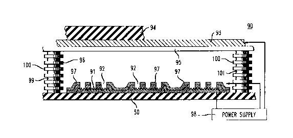
Refernng to the drawings, FIG. 7 is a schematic cross section of an exemplary
field
emission device, here a flat panel display 90, using high breakdown voltage
multilayer
pillars. The device comprises a cathode 91 including plurality of emitters 92
and an anode
93 disposed in spaced relation from the emitters within a vacuum seal. The
anode conductor
93 formed on a transparent insulating substrate 94 is provided with a phosphor
layer 95 and
mounted on support pillars 96. Between the cathode and the anode and closely
spaced from
the emitters is a perforated conductive gate layer 97.
The space between the anode and the emitter is sealed and evacuated, and
voltage is
applied by power supply 98. The field-emitted electrons from electron emitters
92 are
accelerated by the gate electrode 97 from multiple emitters 92 on
2~6~~~~
-5-
each pixel and move toward the anode conductive layer 93 (typically
transparent
conductor such as indium-tin-oxide) coated on the anode substrate 94. Phosphor
layer 95 is disposed between the electron emitters and the anode. As the
accelerated
electrons hit the phosphor, a display image is generated.
Pillars 96 are multi-layer structures comprising alternating layers of
insulator 99 and conductor 100. Preferably the insulating layers 99 are
recessed with
respect to the conductor layers 100 to define a plurality of grooves 101. The
grooved
surface structure increases the breakdown resistance by increasing the surface
distance between the electrodes. In addition, the grooved structure traps many
secondary electrons.
The multilayer structure consisting of alternating layers of dielectric
material and conductive material is particularly advantageous because when
field
emitted electrons from the cathode impinge upon a conductive region, the
undesirable multiplication of outgoing electrons typically seen on insulator
surfaces
is minimized, permitting higher operating voltages, shorter pillars and more
nearly
cylindrical geometry.
II. Pillar Design
There are five considerations in optimal pillar design. First, the optimal
pillar design is one where surface paths on dielectric material from negative
to
positive electrodes are as long as possible for a given height of the pillar.
Second, it
is desirable to construct the pillar so that most secondary electrons will re-
impact the
pillar surface close to the point of their generation, rather than being
accelerated a
substantial distance toward the positive electrode. This goal is advantageous
because most materials generate less than one secondary electron for each
incident
electron if the incident energy is less than SOOV (or more preferably, less
than
200V). Under these conditions, secondary electrons will generally not have
enough
energy to make an increasing number of secondaries of their own. For the
purposes
of this goal, "close" is defined as a point where the electrostatic potential
is less than
SOOV more positive than the point at which the electron is generated, and
preferably
less than 200V more positive. Third, it is desirable to construct the pillar
out of
materials that have secondary electron emission coefficients of less than two,
under
the normal operating conditions. Fourth, it is desirable to have as much of
the
surface of the pillar oriented so that the local electric field is nearly
normal to the
insulator surface, preferably with the field lines emerging from the surface,
so that
secondary electrons will be pulled back toward the surface and re-impact with
energies less than the abovementioned 200-SOOV. It is known that a conical
pillar
2~.6~'51~~
-6-
that has the electric field coming out of the insulator surface at 45 degrees
from the
normal can hold off as much as four times the voltage that a pillar with walls
parallel
to the field will support. Fifth, the pillar must not be so much wider at the
anode end
that it substantially reduces the area that can be allocated to the phosphor
screen.
The pillars in the field emission devices mechanically support the anode
layer above the pillars and electrically separate the cathode and anode.
Therefore,
mechanical strength as well as dielectric properties of the pillar material
are
important. In order to withstand the high electrical field applied to operate
the
phosphor material which is typically coated on the anode plate, the pillar
material
should be an electrical insulator with high breakdown voltage, e.g. greater
than about
2000 V and preferably greater than 4000 V for using the established phosphors
such
as the ZnS:Cu,AI phosphor.
1QI. Fabrication Of Devices Having Multilayer Pillars
Improved pillars can be constructed as illustrated in the flow diagram of
FIG. 2. The first step (block A in FIG. 2) is to prepare a mufti-layered
composite
precursor consisting of alternate dielectric and conductive layers. FIG. 3A
shows an
exemplary precursor 30 comprising alternate conductive layers 31 and
insulating
layers 32. Regions to be cut out as pillar preforms are indicated by the
reference
numeral 33.
A suitable pillar insulating material may be chosen from glasses such as
lime glass, pyrex, fused quartz, ceramic materials such as oxide, nitride,
oxynitride,
carbide (e.g., A12O3, Ti02, Zr02, AII~ or their mixture, polymers (e.g.,
polyimide
resins and teflon) or composites of ceramics, polymers, or metals. A typical
geometry of the pillar is a modified form of either round or rectangular rod.
A
cylinder, plate, or other irregular shape can be used. The diameter of the
pillar is
typically SO-1000 ~.m, and preferably 100-300 p.m. The height-to-diameter
aspect
ratio of the pillar is typically in the range of 1-10, preferably in the range
of 2-5. The
desired number or density of the pillars is dependent on various factors to be
considered. For sufficient mechanical support of the anode plate, a larger
number of
pillars is desirable. However, in order to minimize the loss of display
quality, the
manufacturing costs and risk of electrical breakdown, too many pillars are not
desirable, and hence some compromise is necessary. A typical density of the
pillar
is about 0.01-2~ of the total display surface area, and preferably 0.05-0.5%.
For a
FED display of about 25x25 cm2 area, approximately 500-2000 pillars each with
a
cross-sectional area of 100x 100 p.m is typical.
~21~~50~
-, _
Suitable pillar conductive or semiconductive materials include metals or
alloys (e.g., Co, Cu, Ti, Mn, Au, Ni, Si, Ge) or compounds (e.g., Cu20, Fe203,
Ag 2 O, Mo0 2 Cr 2 03 ). These materials have generally low secondary electron
emission coefficient 8m~ of less than 2, e.g., 1.2 for Co, 1.3 for Cu, 1.1 for
Si, 1.2
for Cu 2 O, 1.0 for Ag 2 O and 1.2 for Mo0 Z. The coefficient is defined as
the ratio of
number of outgoing electrons/number of incoming electrons on a given surface
of
the material. Insulators typically have high secondary electron emission
coefficient
of 2-20, e.g., 2.9 for glass and - 20 for MgO.
In these pillar designs, there is an allowable tradeoff between the
material properties (i.e. 8m~ and the conductivity) and the geometry of the
pillars.
In order to reduce the undesirable multiplication of electrons, it is
necessary that the
average number of secondary electrons that are generated by an incident
electron and
then travel through enough of a potential drop to generate more than one
tertiary
electron be less than unity. We define a tertiary electron as a secondary
electron
produced from a secondary electron that has been accelerated into a surface.
The
secondary electron typically must have 200-1000 eV of energy on impact with
the
surface in order to generate more than one tertiary electron. This threshold
energy is
referred to as Eo, and is available in standard tables for each material.
The conductive materials are incorporated into the multi-layer structure
as follows. A first slurry-like or suspension-like mixture containing a
dielectric
particles such as glass frits, a liquid carrier (water or solvent), and
optionally a
binder such as polyvinyl alcohol is prepared by thorough mixing. A second
slurry-
like mixture containing conductive or semiconductive particles, a liquid
carrier, and
optionally a binder, (and also optionally some dielectric particles such as
glass frits
with preferably less than 60% in volume as compared to the conductor volume)
is
similarly prepared. The desired particles sizes are 0.1-20 ~.m. These two
mixtures
are alternately deposited on a flat substrate using known ceramic processing
technique such as spray coating, doctor blading, etc., with intermediate
drying or
semi-sintering process to form a multilayer composite. Alternatively, thin
sheets of
metal and precursor sheets of binder containing dielectric composite may be
alternately stacked up. A soft metal such as Au is especially desirable
because it is
easy to be cut inside the multilayer, and is resistant to etching by
hydrofluoric acid
typically used for etching of glass type dielectric layer. A thin adhesion-
enhancing
metal film such as Ti may optionally be coated on the surface of the metal
layer.
Another variation in processing is to spray-coat the first mixture on metal
sheets
which are then stacked up.
21~~~0~
-g-
The typical thickness of individual layers is 5-500 pm, and preferably
20-100 ~.m. The overall thickness of the multi-layer composite is in the same
order
as the desired pillar height, typically in the range of 150-2000 p.m.
The second step in FIG. 2 (block B) is to cut out or etch out
approximately pillar-sized preforms. For example, round (or rectangular) rods,
typically 30-300 p.m dia. or plates of 30-300 pm thickness can be cut out from
the
mufti-layer composite by various means such as mechanical cutting, punching
out,
or laser cutting. FIG. 3B illustrates a typical pillar preform 33.
The pillar preforms are then subjected to differential etching treatment
(block C in FIG. 2) so that the dielectric layers are etched out more than the
metallic
layers so as to form the finished pillar of FIG. 3C having grooves 34.
As shown in FIG. l, which shows a pillar 50 with a deep groove 12, not
all secondary electrons 10 will travel far enough to have gained more energy
than Eo
so that they will make more than one tertiary electron 11. Surfaces with deep
grooves 12 (where the depth of the groove d is greater than 0.3 times the
width), are
preferred, and surfaces where the groove depth is greater than the width (d/w
> 1.0)
are especially preferred, because a large fraction of secondary electrons
collide with
the surface before they have acquired much energy. Consequently, materials
with
higher 8m~ require grooves with a greater ratio of d/w. Also as will be
apparent
from FIG. 1, the voltage difference across a groove must be smaller than Eo/q
{q is
the electron charge), for the above argument to hold. Consequently, the
desired
number of grooves along the length of the pillar according to the invention,
is
typically greater than Vq/Eo, and preferably greater than 2Vq/Eo. Thus,
pillars with
large E o require fewer grooves.
The sintering, densification or melting of the dielectric particles in the
first layer and the conductive particles in the second layer, which is shown
in FIG. 2
(block D), can be carried out, either fully or partially, before or after the
differential
etching step. In the case of glass layer and gold sheet composite preform,
hydrofluoric acid preferentially etches the glass resulting in the desired
multilayer,
grooved, pillar geometry with the conductive layer protruding so as to reduce
the
secondary electron emission.
The sintering (or melting) and etching processes may be applied on the
pillar preform either as individual parts, or as many parts simultaneously
placed on
the device substrate or on a carrier tray.
_~16~~0~
-9-
Instead of differential etching, an alternative way of producing the
desired grooved structure is to use differential shrinkage of the first layer
and the
second layer. Depending on the concentration of the slurry mixture, higher
concentration of liquid carrier (to be evaporated later) and binder (to be
pyrolized
later) in the dielectric layer than in the conductive layer will lead to more
shrinkage
in the dielectric layer during densification processing (sintering, melting,
etc.) thus
resulting in the desired, grooved multi-layer pillar structure with recessed
dielectric
layers.
While most of the discussions here have concerned multilayers
consisting of alternating conductive and dielectric layers, the principles of
this
invention may be applied to create a grooved (or corrugated) pillar structure
consisting of two dielectric materials. The two dielectric materials would
have
diferent etch rate or shrinkage rate so that the desired grooves are formed.
The
applicants also consider the possibility of multilayer structure consisting of
three or
more materials as a simple extension of this invention.
The next step, shown as block E of FIG. 2, is to adhere the pillars to a
device electrode, preferably the emitter cathode. This can be done by punching
the
pillar preforms in place on the electrode with a thermally activated adhesive
in place
or by applying the finished pillars with pick-and-place machinery.
FIG. 4 illustrates apparatus useful in making field emission devices in
accordance with the invention comprising an apertured upper die 40, lower die
41
and a plurality of punches 42. The die apertures 43 and 44 are aligned with
positions
on a device electrode 45 (here a cathode emitter) where pillars are to be
adhered, and
a multilayer preform 30 can be inserted between dies 40 and 41. Pillar
preforms 33
are then punched into position on electrode 45. The pillar preforms 33 can be
grooved and adhered to the electrode by the application of heat.
FIG. 5 illustrates an alternative approach in which the pillars are
punched, grooves are formed and then the finished pillars 50 are placed on
electrode 45 by pick-and-place machinery (not shown) where they are adhered as
by
thermally activated adhesive.
FIG. 6 illustrates apparatus useful in the approach of FIG. 5, showing
that the punching arrangement of FIG. 4 can be used to place the punched
pillar
preforms 45 onto a pillar carrier tray 60 for groove formation and
presentation to
pick-and-place machinery.
_ ~~.665~~
- to -
It is to be understood that the above-described embodiments are
illustrative of only a few of the many possible specific embodiments which can
represent applications of the principles of the invention. For example, the
high
breakdown voltage pillars of this invention can be used not only for flat-
panel
display apparatus but for other applications, such as a x-y matrix addressable
electron sources for electron lithography or for microwave power amplifier
tubes.