Note : Les descriptions sont présentées dans la langue officielle dans laquelle elles ont été soumises.
216814~
P1071.AA - 1- Dezember 2(), 1~'~5
ENERGY TR~NSMISSION DEVICE FOR AN OPTOELECTRONIC LAE~EL
BACKGROUND OF THE INVENTION
It is possible, by use of actual means, to realize autonomous optoelectronic
labels having non-volatile memories, which can be supplied with power and
read or read/written from distance as described in the Swiss patent
application ~ 02 120/94-0 dated July 4, 1994. Said patent application focuses
on the optoelectronic devices, which are necessary to operate the label. A
Swiss patent application N 03 759/94-1 dated December 13, 1994 relates to
the procedures for the communication management between the label and
external reading/writing devices. One of the important problems referring to
this communication concerns the energy tr~n~mi~sion devices, which provide
the necessary operation energy, by a distance transmission of light.
SUMMARY OF THE INVENTION
The present invention concerns a device for the tr~ncmi~ion of energy to
supply an optoelectronic label. Said device comprises a luminous energy
source and means allowing to focus said luminous energy source, it comprises
20 pointing devices allowing to detect the label under concern and it comprises
switching devices allowing to operate said energy source.
21 6~1~6
P1071.AA - 2 -
BRIEF DESCRIPTION OF THE DRAWINGS
Figure 1 shows an exemplary embodiment of a device according to the
invention comprising electroluminescent pointing devices.
Figure 2 is an exemplary block diagram showing the switching devices of the
energy source.
Figure 3 shows an exemplary embodiment of a device according to the
invention comprising optic pointing devices.
Figure 4 shows a device according to the invention comprising pointing
devices being associated to image recogrution devices.
DESCRIPTION OF THE PREFERRED EMBODIMENTS
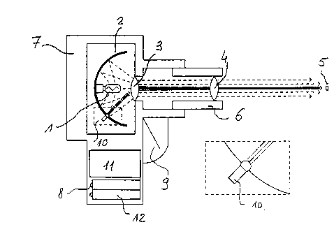
Figure 1 shows an exemplary embodiment of a device according to the
invention having a pistol-like shape. Said device comprises a luminous source
1, being e.g. a halogen bulb like they are used for car headlamps. The light
delivered from said bulb is directed by means of a parabolic reflector 2 to a
25 set of two lenses 3,4 allowing to concentrate said light into the direction of the
label 5. The lens 4 can be mounted in a zoom-like way on a sliding portion 6,
allowing to adjust and focus the light in function of the distance to the label.All this parts are mounted on a moulded case 7, having a pistol-like shape to
be held easily by hand. Said case comprises further a grip 8 and a two stage
30 trigger 9. Moreover, the device comprises a diode laser 10 delivering a fine a
very directive luminous beam like the laser pens which are used by conference
~16814 6
P1071.AA - 3 -
speakers in order to indicate something on a board. Said luminous beam is
directed in direction of the label 5 by means of lenses 3,4. Moreover, the
device comprises a control and switching circuit 11 for the luminous source 1
and the diode laser 10. Said circuit is actuated using the trigger 9. Moreover,
5 the device comprises a power supply source being represented by a battery set
12. It is of course possible to replace said battery set by a set of rechargeable
accllmlll?.tors or by an external power supply source, being connected by a
cable. The device comprises further optoelectronic devices, which are
provided to ensure the communication to the label. Said optoelectronic
10 devices are described in detail in the two above mentioned patent applications
and are, for this reason, not represented here.
The functioning can be described as follows. In order to read the label, the
15 pistol must be directed in the label's direction. The diode laser 10 is activated
by moving the trigger 9 in a first position. A fine and very directive luminous
beam enables a high precision pointing at the label. The detection is
accomplished when a luminous beam of the diode hit the label. The primary
light source 1 is activated by moving the trigger in a second position, allowing20 the power supply and the build up of a communication to the label. At the
end of a desired reading or writing operation, the luminous source is
interrupted. It reveals to be very important to delimit the release of the
primary source to a strict minimum. Firstly, the energy consllmm~tion can be
very important. In order to obtain a good autonomy of the device, the
25 batteries or accumulators must be operated in an economic manner. Secondly,
the bulbs have important heat losses. Long time releases of the primary
source require specialized devices like radiators or ventilators. Thirdly, the
functioning of a plurality of devices, being arranged in a proximity to each
other, can produce undesired interferences.
~16~146
P1071.AA - 4 -
Figure 2 is an exemplary block diagram showing the switching devices of the
energy source and of the diode laser 10. The device has a trigger 9 actuating
onto two interrupters 13, 14. The first interrupter 13 is engaged in a contact
state, by moving the trigger 9 in the above mentioned first trigger position.
S And the second interrupter 14 is engaged in a contact state by moving the
trigger 9 in the above mentioned second trigger position. The switching
devices comprise two D-flip-flops 15, 16. The output Q of the second D-flip-
flop 16 is connected to the input of inverting amplifier 17 and the output of
the inverting amplifier 17 is connected to an AND gate 18. The output of the
10 AND gate 18 is connected to a first OR gate 19 and the output of said OR
gate 19 controls the diode laser 10. At the beginning, the outputs Q of the D-
flip-flops 15, 16 are logically false and the output of the amplifier 17 is
logically true. By moving the trigger, the first interrupter 13 is engaged in a
contact state, connecting said first interrupter to the second input of the AND
gate 18. The outputs of the AND gate 18 and of the first OR gate 19 switch
to logically true, supplying the diode laser 10 and emitting a luminous beam
for pointing at the label. By moving the trigger in a second position, the
second interrupter 14 is engaged in a contact state, connecting said second
interrupter to the input D of the first D-flip-flop 15. The output Q of said D-
20 flip-flop 15 switches to logically true. Moreover, the clock-output C of said D-
flip-flop 15 is connected to a control circuit 20 for receiving a clock signal
generated by said control circuit. Since the output Q of the first D-flip-flop 15
is connected to the clock input C of the second D-flip-flop 16, and since input
D of the second D-flip-flop 16 is positive, the output Q of the second D-flip-
25 flop 16 switches to logically true. As a result, the output of the amplifier 17switches to logically false, the AND gate 18 closes and the power supply to
the diode laser 10 is interrupted. On the other hand, since the output Q of the
second D-flip-flop 16 is connected to the primary luminous source 1, a
logically true output Q of the second D-flip-flop 16 applying a voltage to the
30 primary luminous source 1 and the latter emits light for supplying the label. In
order to generate a time-lag for delimiting the length of the release time of
'~168146
P1071.AA - S -
the primary luminous source, the output Q of the second D-flip-flop 16 is
connected by means of a resistance 21 to an input of a second OR gate 22
and to a capacitor 23. The capacitor 23 is slowly charged by the applied
voltage. After exceeding a certain threshold voltage at the capacitor terminals,5 the output of said OR gate 22 switches to logically true. Since said output isinterconnected to the reset input of the second D-flip-flop 16, the latter is
reset to logically false. As a result, the power supply of the primary luminous
source is interrupted. The primary luminous source, therefore, does not
remain released longer than the length of time previously fixed to e.g. two
10 seconds. In order to restart the device, the trigger must be removed in a wayto set the first D-flip-flop 15 to logically false. The control circuit 20 controls
further the communication between the device and the label. The functioning
of the label is described in detail referring to the two patent applications
mentioned above. Said circuit intervenes on the switching devices in two ways.
15 Firstly, for a communication between the device and the label which lasts
longer than the foreseen two seconds, the control circuit 20 delivers a stop
signal to the second input of the second OR gate 22. Since the latter is
connected to the reset input R of the second D-flip-flop 16, the stop signal
resets said D-flip-flop 16 to logically false. As a result, the power supply of the
20 primary luminous source is interrupted. Secondly, since it is possible to usethe diode laser 10 as transmission means for transmitting information to the
label, and while the primary luminous source is released, the control circuit 20is able to generate impulse trains representing information to be transmitted
to the second input of the first OR gate 19 and from there to the diode laser
25 10. The diode laser is, therefore, used as emitting diode.
Figure 3 shows an exemplary embodiment of a device according to the
invention comprising a solely optical pointing devices. Said optical pointing
30 devices can be similar to the pointing devices being used in cameras 37 and
they can be arranged in a similar way. According to Figure 3, the luminous
216~1~6
P1071.AA - 6 -
source 30, its parabolic reflector 31 and its focusing lenses 33, 34 for focusing
light emitted from the luminous energy source to the label 35. The pointing
procedure is realized in an entirely optical manner, using a combination of
lenses allowing to visualize in a window 36 an image of an object being within
5 the axis of a luminous beam. Therefore, it is possible to center the label using
cross hairs 38 being arranged within said window 36. Since many similar
known systems exist, said optical pointing devices are represented only in a
very schematic manner. Such systems can be provided with their proper
optical devices, or with optical devices being combined with focusing means.
10 Such systems are not used only for photographic purposes but also in derived
systems, e.g. for guns. Moreover, such systems are often passive systems which
consume no energy in contrast to the device according to Figure 1. Such a
passive system can be operated in a permanent manner. A starter 39 enables
to start the luminous source 30 on command. Referring to the embodiments
15 described above, said command is effected m~nll~lly. With reference to the
description of the following figure, it is however possible, to incorporate saidcommand in an automatic procedure.
20 Figure 4 shows a device according to the invention comprising pointing
devices being associated to image recognition devices. The pointing devices
are represented by a charge-coupled device (CCD) camera 40, being directed
to a transfer line 45 provided with labels 35 for an optical reading/writing.
The first one of the above-cited patent application mentions the possibility to
25 associate said labels to targets, which can be registered by optical means. The
CCD 40 camera is connected to digitalization and image analysis means 51,
which are known and used nowadays in many automatized positioning
systems. Such image analysis means 51 enable to deliver a signal for each
received target image 42 and to compare said image with preprogrammed
criteria. Therefore, a target at the center of said image 42 can be compared
with a preprogrammed criteria, e.g. if the target is conform in size and
2168146
P1071.AA 7
dimension with a preprogrammed target image 43. If said necessary
preprogrammed criteria is fulfilled, a corresponding release signal 50 releases
the primary luminous source 44. Other preprograrnmed criteria can stop the
transfer line 45 during the reading/writing operations. According to Figure 4,
5 the pointing devices 40 and the luminous source 44 are arranged in a
physically separated manner. The communication means for a communication
with the label 35 can be integrated within the pointing devices or within the
luminous source or they can be arranged in a physically separated manner.
There are of course many other possible applications for said device according
to the invention, such applications does not, however, bring forward any new
elements.