Note : Les descriptions sont présentées dans la langue officielle dans laquelle elles ont été soumises.
2168520
r
-1-
INVERTER/CHARGER CIRCUIT FOR
UNINTERRUPTIBLE POWER SUPPLIES
TECHNICAL FIELD
The present invention relates to
uninterruptible power supplies and, more
particularly, uninterruptible power supplies
having switch mode converters.
BACKGROUND OF THE INVENTION
The present invention is of particular
importance when employed in the context of an
uninterruptible power supply (UPS) for a cable TV
system, and that application will be discussed in
detail herein. The present invention has broader
application to other environments, however. For
example, coaxial cable networks are being used or
contemplated for use as communications systems
that allow signals to be broadcast from the home
as well as to the home. The scope of the present
invention should thus be determined in accordance
with the claims appended hereto and not the
following detailed description.
In many environments, it is highly desirable
that power be maintained to electrical equipment
even if utility power is disrupted. One such
. environment is a cable TV (CATV) signal
distribution system. In a CATV system, power must
be maintained to line extending amplifiers
dispersed throughout the system to allow the
signal to be propagated throughout the system.
2168520
-2-
Accordingly, UPSs are distributed throughout
the CATV system to provide an AC power signal for
powering the line extending amplifiers even if
utility power is lost. In line mode, the UPS
generates an AC power signal from the utility line
voltage and charges the battery. In converter
mode, the UPS generates the AC power signal from a
battery within the UPS.
Such prior art UPSs comprise a switch mode
converter and a separate switch mode rectifier
configured as a charger. In converter mode, the
switch mode converter generates an AC power signal
from the DC voltage across the battery. In line
mode, the switch mode rectifier generates a signal
for charging the battery.
PRIOR ART
The patents discussed below were uncovered as
part of a professional patentability search
conducted on behalf of the applicant. None of
these patents disclose a power supply that solves
the problems solved by the present invention.
U.S. Pat. No. 5,185,536 (Johnson, Jr.)
discloses the use of the primary winding of a
transformer as part of the inductance in an output
circuit of a UPS.
U.S. Pat. No. 5,172,009 (Mohan) discloses a
UPS having an inverter using an Ii-bridge topology.
U.S. Pat. No. 5,302,858 (Folts) discloses a
battery charger using an H-bridge topology.
U.S. Pat. No. 5,010,469 (Bobry) discloses an
inverter for use in a UPS that operates at high
218520
-3-
voltage in line mode and low voltage in battery
mode.
U.S. Pat. No. 4,748,342 (Dijkmans) discloses
a power supply circuit that generates two DC
voltages from a single AC source.
U.S. Pat. No. 4,748,341 (Gupta) discloses a
UPS employing a transformer having a plurality of
taps connected to the supply voltage. Each tap
has an associated switch to allow selection of a
given tap as appropriate to maintain the output
voltage within a predetermined range.
U.S. Pat. No. 4,745,299 (Eng et al.)
discloses a UPS in which the line voltage is
rectified to obtain a DC signal. This DC signal
and a secondary DC signal generated by a battery
are switched by the same control circuit.
U.S. Pat. No. 4,719,550 (Powell et al.)
discloses a UPS in which AC power signals from a
number of sources are combined at a node from
which an output voltage is derived. When a power
source generates an AC signal, the AC signal is
rectified into a DC signal and then converted back
into an AC signal. When the power source
generates a DC signal, the DC signal is simply
converted into an AC signal and applied to the
common node .
U.S. Pat. No. 3,348,060 (Jamieson) discloses
a UPS having an inverter adapted to permit flow of
current in both directions. The phases of a
waveform generated by the inverter and a source
waveform are shifted to maintain a battery at a
predetermined condition of charge.
-4-
U.S. Pat. No. 3,339,080 (Howald) discloses a converter
circuit that charges a battery when the circuit is connected to
an AC source voltage and to generate an AC signal for supplying
power to a load when not connected to the source signal.
U.S. Pat. No. 3,293,445 (Levy) discloses a power supply
circuit in which the battery is arranged in series with an AC
power source. The battery is charged by the AC source when
present and supplies power to the load when the AC power source
is not present.
U.S. Pat. No. 4,763,014 (Model et al.) discloses a switch
that is controlled to prevent reverse power flow.
U.S. Pat. No. 5,057,698 (Widener et al.) discloses a power
supply having a current shunt that reduces output current to zero
as the operating frequency of the converter moves to a
predetermined frequency.
U.S. Pat. No. 5,198,970 (Kawabata et al.) discloses a UPS
having an inverter using an H-bridge topology.
SUMMARY OF TH$ INVLNTION
From the foregoing, it should be clear that primarily the
present invention seeks to provide improved uninterruptible power
supplies.
Another more specific aspect of the present invention seeks
to provide a UPS having a favourable combination of the following
characteristics:
(a) may be used in a coaxial cable network for transmitting
CATV and communications signals;
CA 02168520 2001-03-19
_5_
(b) recit.rce the number and cost of parts
necessary to implement a UPS circuit;
(c) reduce the cost of the transformer used
by the UPS circuit;
(d) allow certain relatively expensive parts
to be used both by the inverter portion of the UPS
and the charger portion of the UPS;
(e) implement power factor correction while
charging the battery of the UPS.
Other aspects of the present inventior_ wi7_1
become apparent from the following detailed
description and claims.
These and other aspects are achieved by the
present: invention, which is an uninterruptible
power ~~upply system basically comprising a
transfornner, a switch circuit, a charger control
circuit., an converter control circuit, a control
logic circui.t., and a battery. The transformer
comprises inductively coupled first and second
primary wincii.ngs and a secondary winding isolGted
f rom the f iz:-st and :second windings by a magneti c
shunt. AC lane voltage is connected to the first
primary wincaing, while t:he switch circuit vs
connected t~.~ the second primary winding . ':'he
secondary winding is connected to output
terZninals .
Ire lin« mode, the switch circuit operate:
under the control of the charger control c_rcui~.
to charge the battery. In inverter mode, ~:'ze
switch ci rc~iit operate_~ under the cont_rcl .,_. ;_=__
CA 02168520 2001-03-19
216520
-6-
inverter control circuit to generate a signal from
which the AC power signal may be generated. The
control logic circuit controls which of the
charger control circuit and the inverter control
circuit controls the switch circuit.
With the UPS system configuration just
described, certain switches in the switch circuit
may be used both during charger mode and during
inverter mode. Further, the second primary
winding is also used both during inverter mode and
charger mode. Because the UPS circuit uses one
winding and certain switches in both inverter and
charger modes, a significant reduction in the
parts necessary to implement the UPS function is
achieved.
Further, the transformer configuration
employed eliminates the need for a pair of
inductors used by prior art UPSs when they are
operating in charger mode. These inductors are
relatively expensive, and the elimination thereof
results in a significant reduction in the overall
cost of the UPS circuit.
Additionally, the cost of the transformer
when configured as described above can be
minimized because each of the three windings
comprises a single bobbin formed of only one gauge
of wire. The three bobbins employed to create the
transformer of the present invention are thus
easily and inexpensively manufactured without the
need to change the gauge of the wire during
fabrication of the windings.
The control logic circuit is configured to
allow the switches in the switch circuit to be
.w 21 d8520
controlled by the inverter control circuit when
the UPS is in inverter mode and the charger
control circuit when the UPS is in line/charger
mode. The charger control circuit controls the
switches in the switch circuit in a manner that
creates a DC voltage for charging the battery from
the utility line voltage with power factor
correction.
BRIEF DESCRIPTION OF THE DRAWINGS
FIG. 1 is a block diagram depicting an
exemplary environment in which a UPS constructed
in accordance with, and embodying, the principles
of the present invention may be employed;
FIG. 2 is a block diagram depicting a UPS
circuit constructed in accordance with, and
embodying, the principles of the present
invention;
FIG. 3 is a block diagram showing the
effective circuit obtained when the UPS circuit
described in FIG. 2 is placed in line/charger
mode;
FIG. 4 is a block diagram showing the
equivalent circuit obtained when the UPS circuit
depicted in FIG. 2 is placed in inverter mode;
FIG. 5A is an isometric view depicting a
transformer constructed in accordance with, and
embodying, the principles of the present
invention;
FIG. 5B is a somewhat schematic view
depicting in more detail the construction of the
transformer shown in FIG. 5A;
_ g _
FIG. 6 is a timing diagram depicting an exemplary switch-
over from line/charger mode to inverter mode and back to
line/charger mode;
FIG. 7 is a timing diagram depicting the wave forms employed
to generate the inverter drive signal;
FIG. 8 is a circuit diagram showing details of the switch
array depicted in FIGS. 2 and 4;
FIG. 9 depicts the switch circuit of the effective circuit
shown in FIG. 3;
FIG. 10 shows the detail of construction and operation of
the drive circuits shown in FIGS. 8 and 9, FIG. 10 being
comprised of FIGS. 10A and 10B;
FIG. 11 depicts an exemplary microcontroller that can be
used to implement the inverter control circuit portion of the UPS
circuit depicted in FIG. 2;
FIG. 12 is a schematic circuit depicting the details of
construction of the control logic circuit shown in FIG. 2;
FIG. 13 is a schematic diagram depicting the details of
construction of the charger control circuit shown in FIG. 2, FIG.
13 being comprised of FIGS. 13A and 13B.
CA 02168520 2001-03-19
2ib8520
_g_
DETAILED DESCRIPTION
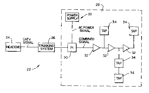
Referring initially to FIG. 1 of the drawing,
depicted therein is an exemplary power supply
circuit 20 constructed in accordance with, and
embodying, the principles of the present
invention. In FIG. 1, the power supply circuit 20
is shown in the context of a CATV system 22.
In addition to the power supply 20, the CATV
system 22 comprises a head end 24, a trunking
system 26, a power inserter 28, a plurality of
line extending amplifiers 30, and a plurality of
taps 32. The power supply 20, power inserter 28,
line extending amplifiers 30, and taps 32 form a
local distribution portion 34 of the CATV
system 22.
The head end 24 generates a CATV signal from
a variety of sources. The trunking system 26
carries the CATV signal to the local distribution
portion 34.
Within the local distribution 34, the power
supply 20 generates an AC power signal. The power
inserter 28 combines the AC power signal and the
CATV signal to obtain a combined signal. The line
extending amplifiers 30 amplify the CATV signal
portion of the combined signal using power
obtained from the AC power signal portion thereof.
The taps 32 are arranged to pass only the CATV
signal to one or more subscriber residences (not
shown) physically located near the taps.
While not shown in the exemplary CATV
system 22, it should be understood that a
plurality of power supplies such as the power
2id8520
-10-
supply 20 may be arranged throughout the local
distribution portion 34. The exact location of
these power supplies is based on factors such as
the availability of utility line voltage, signal
5 strength, and the distance between the subscribers
residences within the local distribution area.
Referring now to FIG. 2, the UPS circuit 20
will be described in further detail. This
circuit 20 basically comprises a utility connect
circuit 36, a transformer 38, a charger control
circuit 40, a system control circuit 42, a control
logic circuit 44, a switch circuit 46, and a
battery 48.
The utility connect circuit 36 comprises a
15 line terminal 50 adapted to connect to the utility
connection, an EMI filter 52, and a disconnect
relay 54. These components 50, 52, and 54 are
conventional. As will be described further below,
the disconnect relay 54 is closed when the UPS
20 circuit 20 is in a line/charger mode and open when
the UPS circuit 20 is in a inverter mode.
The system control circuit 42 comprises a
condition detect circuit 56 and a
microcontroller 58. The condition detect
25 circuit 56 samples the utility line voltage and
generates a LINE CLK signal and a LINE DET signal.
The LINE CLK signal indicates the frequency and
phase of the utility line voltage, while the
LINE DET signal is high when the utility line
30 voltage is present and low when the utility line
voltage is not present or out of certain
predetermined limits. The condition detect
circuit 56 also generates a SCALED FEEDBACK signal
2168520
-11-
based on a SYSTEM FEEDBACK signal that is an
analog of the output signal. The condition detect
circuit 56 is basically conventional and will not
be described herein in further detail.
The microcontroller 58 monitors the LINE DET
signal and, based on this signal, determines
whether the UPS circuit 20 should be in
line/charger mode or in inverter mode. The
' microcontroller 58 energizes and thus closes the
disconnect relay 54 when the UPS circuit 20 is in
the line/charge mode and deenergizes the
disconnect relay 54 when the UPS circuit 20 is in
the inverter mode.
The microcontroller 58 further generates an
INV ON signal and a CHGR ON signal. In
particular, the INV ON signal is high when the UPS
circuit 20 is in the inverter mode and low when it
is in the line/charge mode. The CHGR ON signal,
on the other hand, is high when the UPS circuit 20
is in the line/charge mode and low when it is in
the inverter mode.
Additionally, the microcontroller 58
generates INV A and INV B signals for controlling
the switch circuit 46 when the UPS circuit 20 is
in inverter mode. In response to a CHARGER ON/OFF
signal generated by the control logic circuit 44,
the charger control circuit 40 generates a CHARGER
DRIVE signal.
Under the control of the INV ON and CHGR ON
signals, the control logic circuit 44 passes
either the INV A and INV B signals generated by
the microcontroller 58 or the CHARGER DRIVE signal
2168520
-12-
generated by the charger control circuit 40 as the
DRV1, DRV2, DRV3, and DRV4 signals.
As will be described in detail below, the
switch circuit 46 comprises four switching devices
arranged in a H-bridge configuration. The DRV1,
DRV2, DRV3, and DRV4 control the switching devices
in the switch circuit 46. Under the control of
these signals, the switch circuit 46 either
develops a signal appropriate for charging the
10 battery 48 when the UPS circuit 20 is in
line/charge mode or develops a pulse width
modulated power signal from which a stand-by AC
power signal may be generated.
Referring now to FIGS. 2, 5A, and 5B, it can
be seen that the transformer 38 basically
comprises first primary windings 60, second
primary windings 62, and secondary windings 64.
The primary windings 60 and 62 are arranged on a
magnetic core 66. A magnetic shunt 68 is arranged
20 between the secondary windings 64 and the primary
windings 60 and 62.
The first primary winding 60 comprises first
and second terminals 60a and 60b that are
electrically connected to utility power through
25 the utility connect circuit 36. The second
primary windings 62 comprises first and second
terminals 62a and 62b that are electrically
connected to the switch circuit 46 as will be
described below in further detail. The secondary
30 windings 64 comprise first and second terminals
64a and 64b and a center tap 70. A ferroresonant
capacitor 72 is electrically connected across the
first and second terminals 64a and 64b. First and
~~ X85
-13-
second output terminals 72 and 74 are electrically
connected between the center tap 70 and second
terminal 64b of the secondary winding 64,
respectively.
With the arrangement just described, the
transformer 38 operates as a ferroresonant
transformer, although the input windings 60 and
inverter/charger windings 62 have a linear
relationship. In a basic form, however, the
present invention may also be used in a power
supply employing a linear transformer.
In the exemplary transformer 38, an AC power
signal across either of the first primary winding
60 will result in a linearly related AC signal
across the second primary windings 62. An AC
signal across either of the primary windings 60
and 62 results in a non-linearly related AC power
signal across the secondary windings 64.
In line/charger mode, AC line voltage is
applied to the first primary winding 60, resulting
in an AC power signal across the output terminals
72 and 74. The output terminals 72 and 74 are
connected to the power inserter 30 shown in FIG. 1
such that the AC power signal thereacross may be
used by the line-extending amplifiers 32 as
described above. Additionally, the line voltage
across the first primary winding 60 results in an
AC voltage across the second primary winding 62
that is provided to the switch circuit 46 to
charge the battery 48.
When the UPS circuit 20 is in its inverter
mode, the inverter power signal generated by the
switch circuit 46 and battery 48 is present across
z ~ 6~5zo
-14-
the second primary windings 62. This results in
an AC power signal being generated across the
output terminals 72 and 74.
Referring now to FIGS. 3 and 4, the effective
circuits obtained when the UPS circuit 20 is
placed in line/charger mode and inverter mode will
be explained. In particular, FIG. 3 shows the
effective circuit obtained when the UPS circuit 20
is placed in line/charger mode. In line/charger
mode, the microcontroller generates the CHRG ON
signal to direct the control logic circuit 44 to
generate the charger ON/OFF signal and pass the
charger drive signal as the DRV2 and DRV4 signals.
The switch circuit 46, under the control of the
DRV2 and DRV4 signals, charges the battery 48.
The microcontroller 58 further energizes the
disconnect relay 54 to pass the line voltage
through to the input windings 60 of the
transformer 38.
Referring now to FIG. 4, depicted therein is
the UPS circuit 20 in inverter mode. In inverter
mode, the microcontroller 58 deenergizes the
disconnect relay 54 to prevent line voltage from
reaching the input windings 60 and prevent power
from being fed back to the utility power grid.
At the same time, the microcontroller 58
generates an INV ON signal that instructs the
control logic circuit 44 to pass the INV A and
INV B signals as the DRV1, DRV2, DRV3, and DRV4
signals. These signals, in turn, control the
switch circuit 46 to develop the inverter power
signal described above from the DC voltage present
across the battery 48. As described above, the
.~ 2168520
-15-
transformer configuration thus results in an AC
power signal being present across the output
terminals 72 and 74 having the same frequency as
the inverter power signal.
Referring again to FIGS. 5A and 5B, the
transformer 38 will be described in further
detail. These figures show that the input
windings 60 and the inverter/charger windings 62
are spaced from each other a distance greater than
or equal to four millimeters. The
inverter/charger windings 62 are further spaced
from an end wall 78 of the core 66 a distance
greater than or equal to four millimeters.
This physical configuration allows leakage
inductance between the primary winding 60 and 62
and obviates the need for separate inductors for
the switch mode rectifier during line/charger
mode.
Additionally, FIG. 5B shows that the magnetic
shunt 68 is arranged between the input windings 60
and the output windings 64. As is well-known in
the art, the magnetic shunt 68 establishes a
magnetic path when the ferroresonant transformer
is saturated.
FIG 5B also shows that an alternative center
tap 76' may be provided to allow the UPS
circuit 20 to operate in environments using AC
power signals of different amplitudes.
Indicated at 80 in FIG. 5B are taps from
which the SYSTEM FEEDBACK signal discussed above
may be obtained.
Referring now to FIG. 6, depicted therein is
a timing diagram showing the status of several
___ 2 ~ ~b
-16-
signals throughout the UPS circuit 20 as the
circuit 20 changes from line/charger mode to
inverter mode and from inverter mode back to
line/charger mode.
At time t1 the line voltage fails or goes out
of the predetermined limits. The charger ON
signal immediately goes low and the disconnect
relay 54 is deenergized to disconnect the utility
line from the input windings 60. A short delay
time thereafter, the inverter is switched ON. In
the exemplary UPS circuit 20, this delay is set at
96 microseconds, but may range from a minimum of
microseconds up to approximately 100
microseconds without adversely affecting the
15 components using the AC power signal generated by
the UPS circuit 20.
As long as the line failure persists, the UPS
circuit 20 is in inverter mode and generates the
AC power signal from the DC voltage across the
20 battery 38.
At a point indicated by reference
character t2, the line voltage is restored. The
UPS circuit 20 remains in inverter mode for five
additional seconds to ensure that the restoration
of the line voltage is not temporary.
After this five second delay, the
microcontroller 58 begins to synchronize the AC
power signal with the line frequency to prepare
for the changeover from inverter mode to
line/charger mode. When these signals are
synchronized at time t3, the disconnect relay 54
is energized to connect the line voltage to the
input windings 60. Eight milliseconds later, the
218520
l,
_ 1 7 -
inverter is turned off and sixteen milliseconds
after time t3, the charger ON signal goes high to
allow the line voltage to charge the battery 48.
FIG. 7 depicts certain voltage waveforms in
the UPS circuit 20 when the circuit 20 is in
inverter mode, with the inverter power signal
being shown at the bottom of this drawing. The
generation of a inverter power signal such as that
shown in FIG. 7 is fairly conventional and will
not be discussed herein in detail.
Referring now to FIG. 8, depicted therein in
further detail is the switch circuit 46 described
briefly above. The switch circuit 46 basically
comprises four power MOSFETs 82, 84, 86, and 88
with integral diodes 90, 92, 94, and 96.
FET drive circuits 98, 100, 102, and 104 are
associated with the MOSFETs 82, 84, 86, and 88,
respectively. Comparing FIGS. 7 and 8, it can be
seen that the drive control signals DRV1, DRV2,
DRV3, and DRV4 are sent to the driver circuits 98,
100, 102, and 104. The waveforms shown in FIG. 7
develop the inverter power signal waveform also
shown in FIG. 7 at the terminals DOT and UN DOT
shown in FIG. 8. These terminals are in turn
electrically connected to the terminals 62a and
62b of the inverter/charger windings 62.
Referring now to FIG. 9, the switch
circuit 46 is shown therein in line/charger mode.
The effective circuit shown in FIG. 9 results in
the drive signals DRV1 and DRV3 turning off the
switches 82 and 86 shown in FIG. 8. The drive
control signals DRV2 and DRV4 are turned on and
off simultaneously at 50 kH. The pulse width of
21b8520
-18-
these signals DRV2 and DRV4 are modulated under
the control of the charger drive circuit 40 to
develop a signal across the battery terminals that
is within the specifications for the particular
battery being charged in a given set of
environmental conditions. As will be described in
further detail below, this arrangement allows the
battery to be charged with integral power factor
correction.
Referring now to FIG. 10, depicted at 106
therein is an exemplary switch circuit comprising
the switch drive circuit 100, switch element 84,
and diode 92 shown and described above. This
circuit 106 is the same as those associated with
the switch elements 82, 86 and 88 described above.
Accordingly, only the switch circuit 106 will be
described herein in detail.
As. shown in FIG. 10, the switch drive circuit
100 basically comprises an input/isolation
portion 108, a current limiting portion 110, and a
drive portion 112.
The drive signal DRV2 that controls the
switch element 84 is applied across a level
shifting circuit formed by resistors 114 and 116.
An isolating element 118 and its associated
capacitors 120, 122, 124, 126 and diodes 128 and
130 isolate the control logic circuit 44 from the
high voltages applied across the switching
elements 84.
The current limiting circuit 110 comprises
capacitors 132 and 134, resistors 136, 138, 140,
and 142, diodes 144 and 146 and a FET switch 148.
The current limiting circuit 110 is basically
2168520
,.
-19-
conventional and is designed to turn off the
switching elements 84 when the current
therethrough exceeds a predetermined amount.
The switch drive portion 112 comprises
resistors 150 and 152 and diodes 154 and 156 to
provide smooth turn on and fast turn off of the
switch elements 84. A resistor 158 and Zener
diode 160 limit the voltage applied across the
switch elements 84. A resistor 162 is provided to
buffer the signal applied to the switch
elements 84.
At this point, it should be noted that the
switch element 84 comprises two MOSFETS with
integral rectifying diodes 92 in parallel,
although one or more such MOSFETS may be used
under different circumstances. It is also not
necessary that the MOSFETS and diodes be
integrally packaged.
Finally, a snubber circuit is formed by a
capacitor 164 and resistor 166.
Turning now to FIG. 11, the microcontroller
58 is shown in further detail. The
microcontroller 58 is a conventional integrated
circuit chip and comprises a microprocessor,
random access memory (RAM) and read only memory
(ROM). In the exemplary UPS circuit 20, a chip
sold by Motorola under Part No. 68HC711E9FN is
used. The operation of the software contained
within this chip is described above with reference
to FIGS. 6 and 7 and will not be described again
in further detail.
FIG. 12 shows the details of construction of
the control logic circuit 44 described above.
- ~ ~ 6~~~0
,,
-20-
The INV A, INV B, INV ON, and CHGR ON signals
described above are received by inverters 168,
170, 172, and 174, respectively. These inverters
168-174 ensure that the micro signals are shifted
to the appropriate level to drive the logic
elements remaining in the control logic
circuit 44.
The INV A and INV B signals are initially
passed through a NOR gate 176 and AND gate 178
(INV A) and AND gate 180 and NOR gate 182 (INV B).
In conjunction with RC circuits 184 and 186, these
gates 176-182 develop the DRV1, DRV2, DRV3, and
DRV4 signals described above. The delay provided
by the RC circuits 184 and 186 cause the DRV1-DRV4
signals to have leading and trailing edges that
prevent shoot-through of the switching elements
controlled thereby. The values of resistors 188
and 190 and capacitors 192 and 194 are selected to
provide approximately 1.5 microsecond of delay,
although the specific delay is not crucial.
The outputs of the components 176-182 are
directed to AND gates 196-202. The INV ON signal
is applied to the other input of these AND
gates 196-202 such that the outputs of the
components 176-182 are passed by the AND
gates 196-202 only when the INV ON signals is
high.
Referring now for a moment to the bottom of
FIG. 12, it can be seen that the CHGR ON signal is
applied to one input of an AND gate 204 and, as
will be discussed below, applied to the charger
drive circuit 40. The other input of the AND
gate 204 is the CHARGER DRIVE signal generated by
z ~ ~~~z~
-21-
the charger drive circuit 40. The CHARGER DRIVE
signal is thus passed by the AND gate 204 only
when the CHGR ON signal is high.
The output of the AND gate 204, along with
the outputs of the AND gates 198 and 202, are
applied to OR gates 206 and 208. The outputs of
the AND gates 196 and 200 described above are
further applied to AND gates 210 and 212, while
the outputs of the OR gates 206 and 208 are
applied to AND gates 214 and 216.
The other inputs of these AND gates 210-216
is generated by a lock-out circuit 218. This
lock-out circuit 218 comprises an AND gate 220 and
a NOR gate 222 that result in a low signal
whenever both the INV ON and CHGR ON signals are
high at the same time. The lock-out circuit 218
and AND gates 210-216 thus prevent the uncertain
state that would result at the outputs of the OR
GATES 206 and 208 from being transmitted to the
switch elements controlled thereby.
Accordingly, when the UPS circuit 20 is in
the inverter mode, the outputs of the NOR
gate 176, AND gate 178, AND gate 180, and NOR
gate 182 are present as the drive signals DRV1,
DRV2, DRV3, and DRV4 at the AND gates 210, 214,
212, and 216. When the UPS circuit 20 is in
charge/line mode, the charger drive signal at the
input of AND gate 204 becomes the drive signal
DRV2 and DRV4 at the outputs of the AND gates 214
and 216; in this case, the DRV1 and DRV3 signals
are held low.
Referring now to FIG. 13, the charger drive
circuit 40 will now be described in further
21~~~2~
-22-
detail. At the heart of this circuit 40 is an
integrated circuit chip 224 specifically designed
to generate a PWM signal for charging a battery
with power factor correction. In this case, the
PWM signal is generated at pin 16 of the chip 224
and is referred to herein as the CHARGER OUTPUT
signal. The CHARGER ENABLE signal described above
is applied to pin 10 of the chip 224.
Basically, the chip 224 samples the line
voltage and current and generates the power factor
corrected charger output signal based on the
sampled line voltage and current.
In particular, the line voltage is applied to
coupling capacitors 226 and 228 and full wave
rectified by an element 230. Resistors 232 and
234 maintain symmetry of the full wave rectified
signal. This signal is then applied to pin 6 of
the chip 224 through a resistor 236.
The current through the charger winding is
rectified by a diode bridge 238 to obtain a
voltage signal across a resistor 240 corresponding
to the charger winding current. This voltage is
then applied to terminal 4 of the chip 224 through
a resistor 242.
Resistors 246 and 248 set a voltage limit,
while capacitors 250 and 252, resistors 254, 256,
258, and variable resistor 260 establish a current
limit. A resistor 262 and capacitors 264 and 266
provide compensation for the operational amplifier
within the chip 224.
A capacitor 268 and resistor 270 set the
frequency of the PWM signal. Capacitors 272, 274,
276, and 280 are filters.
- 21b8520
-23-
To provide temperature compensation, a signal
CHRGV-PWM is provided to the positive terminal of
an operational amplifier 282 through a
resistor 284 and across a capacitor 286. The
operational amplifier 282 forms a voltage follower
that develops a DC signal which is proportional to
the CHRGV-PWM signal input thereto. As will be
discussed below, the signal generated by the
amplifier 282 provides temperature compensation.
A resistor 284 and capacitors 286 and 288
provide voltage compensation for the voltage error
amplifier within the chip 224. This compensation
is based on the voltage generated by a voltage
divider comprising resistors 290 and 292 and a
variable resistor 294. By varying the resistance
of the variable resistor 294 or the output of the
amplifier 282 based on the CHRGV-PWM signal, the
voltage level of the switch circuit 46 for a given
battery under a given set of operating conditions.
The present invention may be embodied in
other specific forms without departing from the
essential characteristics thereof. The present
embodiments are therefore to be considered in all
respects as illustrative and not restrictive, the
scope of the invention being indicated by the
appended claims rather than by the foregoing
description; and all changes which come within the
meaning and range of equivalency of the claims are
therefore intended to be embraced therein.