Note : Les descriptions sont présentées dans la langue officielle dans laquelle elles ont été soumises.
2169792
- 1 -
APPARATUS AND METHOD FOR MEASURING VERY ACCURATELY
THE TIME OF AN EVENT
BACKGROUND OF THE INVENTION
1. Field of the Invention
The present invention relates to chronometry, that is
generally the measurement of time but particularly the very
accurate timing of an event relative to clock signals
One of the aspects of chronometry is the timing of an event
in relation to a time reference.
It is known for this chronometry to be carried out
electronically, but it is particularly difficult when very
great accuracy is necessary, as for example for the
chronometry of the arrival of laser beams for measuring
distance or for other time based operations such as the
synchronisation of distant clocks.
An event may be considered in this case as a transition of
an electrical signal detecting the arrival of a laser beam
from a low to a high level. The starting point of the
chronometry is assumed to be known.
2, Description of Prior Art
Patent specification FR-B-2 492 563 and more particularly
FR-B-2 493 553 describe solutions in which the conceivable
accuracy is below a nanosecond, as well as other
applications where this accuracy is desired.
In the latter of the aforesaid specifications an apparatus
is proposed which comprises:
2169792
- 2 -
- a clock providing a time reference,
- means pulsed by the clock, for carrying out a primary
chronometry from an event to a nearby clock cycle,
- logic means for generating a timing pulse associated
with the timing space between the event and a clock pulse
having a position known with respect to the event,
- a constant time circuit receiving the timing pulse to
generate in response an electrical signal of a duration
greatly superior to that of the timing pulse, and
- means for measuring a physical value relative to the
electrical signal and representative of the duration of the
timing pulse thereby enabling a secondary chronometry of
the event.
According to FR-B-2 493 553, the timing pulse starts with
the event and ends with the following clock pulse. The
constant time circuit is a double integrator using the
rapid charge of a capacitor during the timing pulse,
followed by a slow discharge. The discharge time defines
a second timing pulse. The circuit can be adjusted so that
the duration of the second timing pulse is increased
according to a known rule, approximately monotonically by
a relationship having a duration of the first timing pulse
(whence the timing extension). A secondary counter then
measures the duration of the second pulse which provides
the secondary fine chronometry of the event preferably
relative to the same clock.
SUMMARY OF THE INVENTION
The present invention has an object to provide a method and
an apparatus whereby a greater accuracy is achieved below
a hundred and preferably below ten picoseconds, more
specifically it is an object of the present invention to
firstly provide, the logic means adjusted to produce a
~~ 69 792
- 3 -
timing pulse which commences at a time associated with the
event and finishes at a clock pulse which is at least the
second one after its start. Consequently, the duration of
the timing pulse is greater than or equal to a clock period
T0. It is comprised between TO and (k+1) .TO, where k is at
least equal to 1.
In a further object, the constant time circuit is a filter
of selected characteristics, having a time constant greater
than, in principle much greater than, the nominal duration
of the timing pulse.
In a yet further object the measuring means operate on a
chosen portion of the response of the filter for the timing
pulse.
Preferably the filter is a low pass filter, the portion
chosen for the response is around the maximum of the
response and it may be observed that the amplitude of this
portion is thus representative of the duration of the
timing pulse.
BRIEF DESCRIPTION OF THE DRAWINGS
Other features and advantages of the invention will appear
with reference to the detailed description hereafter as in
the accompanying drawings, in which:-
- Figure 1 is a simplified electrical diagram of one
embodiment of the present invention;
- Figure 2 is a detailed diagram of the logic unit 2 of
Figure 1;
- Figure 3 shows four wave form diagrams which
correspond to each other and which are useful for the
understanding of Figure 1;
2.~697~~
- 4 -
- Figure 4A to 4C are three groups of wave form diagrams
for explaining the calibration of the device of the
invention;
- Figure 5 is a detailed arrangement of a group of
elements FPB, APO and SB corresponding to the embodiment of
Figure 1; and,
- Figure 6 is a wave form timing diagram explaining the
operation of the device of the invention as regards the
arrangement of Figure 5.
The accompanying drawings have a number of elements of a
certain character which is difficult to define completely
by the text. Consequently, these are an integral part of
the description and may assist in defining the invention.
DESCRIPTION OF THE PREFERRED EMBODIMENTS
It has already been indicated that the invention concerns
very fine chronometry. In the desired scale of under a
nanosecond it is only possible to time an event after a
determined reference instance which is humanly perceptible
when it is substantially greater than a nanosecond.
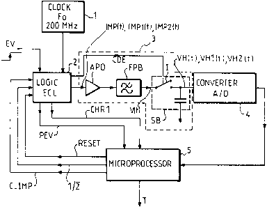
In Figure 1, the circuit has a clock 1 operating at a
frequency Fo which is for example 200 MHZ. This clock has
a stability suitable for the required accuracy, which is
here considered attainable by the man skilled in the art.
The signal transmitted by this clock, serves as the first
input signal for unit 2 which includes the logic circuits.
This unit 2 has as a second input EV, a second electrical
signal, which is stepped. The stepped signal EV represents
a time. The step represents for example the slope time of
a photodetector receiving a laser beam.
~16979~
- 5 -
In a particularly effective embodiment, the present
invention sets out to achieve a timing accuracy of 2 to 3
picoseconds (RMS) for an electrical stepped signal where
the slope time is some 200 picoseconds.
In view of the desired accuracy, it is proper to use
electronic logic circuits which switch very rapidly. For
this reason the logic circuits assembled in unit 2 use ECL
technology.
To describe unit 2 in more detail see Figure 2 where the
logic components are shown as boxes and are of the flip-
flop type.
For the reason already indicated, the embodiment first
starts with a primary count. For this purpose, part 21 of
unit 2 has a counter 210 , receiving at a first input CLK
impulses of frequency Fo and for a period To = 1/Fo coming
from clock 1. The start of the counting commences at a TRF
instant, defined also by a step signal or a pulse to
validate counter 210. Counting stops at the moment when a
signal representing step EV is applied to the second input
PRE of counter 210, having been routed through components
FF1, CL3, FF3 and FF2.
At an appropriate moment the state of the counter is
retained for example in a register 212, which is in this
case suitable to provide a digital signal CHIti,
representing the primary chronometry, in principle which is
not ambiguous but where the accuracy is limited by the
period of the clock To. The method, of transferring the
state of counter 210 in register 212 can depend on whether
the counter 210 is synchronous or asynchronous. This
effect of the indicators may be found in FR-2 492 563,
already cited.
- 6 -
This is described in relation to the first four lines of
the chronogram of Figure 3. In the example shown, timing
step EV (third line from the top) occurs during the N'th
state of counter 210, from reference time TRF. The
numerical value CHRl is deducted by means of synchronous
command PRE and N or N+1 according to the construction of
part 21.
Logic unit 2 also comprises a stage 22, the function of
which is to generate a timing pulse IMP(t) (more precisely
an electrical signal forming a timing pulse), associated
with the timing space between event EV and a clock pulse of
known position relative to this event. IMP(t) results from
a logical operation carried out by logic component CL1,
between step EV from FF1 and the signal from the third
flip-flop component FF3 which represents the positional
clock pulses produced by clock 1. IMP(t) is shown on the
last line of Figure 3.
In this example, the clock pulse with a known position
corresponds to the N+2'th pulse of clock 1, that is the
second clock pulse following step EV. The timing pulse,
referenced IMP(t) is thus obtained.
But, FF3 delivers also at a second output, a signal CDEO
the rising leading edge of which coincides with the end of
the timing pulse IMP(t). This pulse CDEO is applied to the
first input ARM of a digital delay circuit 228 suitable to
provide a timing delay TE, and where the time basis is the
signal from clock 1 applied on its second input CLK which
provides at an output of delay circuit 228 a signal CDE
which commands the sampling of the event which will be
described below.
- 2~.69'~9~
_,_
After generating pulse IMP(t) by a step EV, the output Q of
FF1 is maintained at 0 due to the memory of FF2, which has
the effect of ignoring any later steps EV as long as a
RESET=1 command has not been sent.
Preferably unit 2 also has a sub-assembly 23 to generate
two calibration pulses referenced IMP1(t) and IMP2(t), of
a duration To and 2To respectively. This sub-assembly 23
has more particularly two flip-flop components FF4 and FFS,
respective outputs of which are coupled by a second logic
component CL2 which passes the resultant logic operations
to FF3.
The synthesis of the calibration pulses takes place when
the input EV is deactivated, that is to say after an
impulse IMP(t) and before the RESET=1 command (the outputs
Q of FFl and FF2 are then at 0). This synthesis is
commanded by a rising front of a signal C IMP and the
choice of IMP(t) or of IMP2(t) depends on the state of
signal 1/2:
- if 1/2=1: output Q of FF5 is held at 0 and IMP(t) is
generated by FF3, FF4, CL2 and CL3 via CL1.
- if 1/2 - 0 : FF5 is active and the double length
impulse IMP2(t) is generated by FF3, FF4, FFS, CL2 and
CL3 via CL1.
The control signals C IMP, 1/2 and RESET are outputs from
a microprocessor 5 which will be described below.
As shown in Figure 4 pulses IMP(t) and IMP2(t) enable the
provision of a frame of the duration of pulse IMP(t).
Thus pulse IMP(t) (Figure 4B) corresponds to the minimum
duration of IMP(t) which is a period To of a clock. Whilst
- g -
pulse IMP2(t) (Figure 4C) corresponds to the maximum
duration of III (t) which is a period 2To.
Returning to Figure 1, the three signals IMP(t), IMP1(t) or
IMP2(t) are available in the same way, the sequence being
controlled by microprocessor 5 as will be described.
The pulse at the output of the logic unit ECL 2 is applied
to an amplifier APO, followed by a low pass filter FPB,
then a memory circuit SB, which is preferably a sample-and-
hold circuit or a track-and-hold circuit.
The filter, amplifier and memory circuit are described in
more detail in Figure 5.
The pulses are first of all applied to a circuit 30 which
comprises a limiting amplifier having a current output. A
transistorised differential amplifier may be used.
The output of stage 30 is applied to a first filter stage
31. It has a resistor 310 of value R1, a capacitor 311 of
value C1 and an amplifier 315. The amplifier chosen in
this example is a rapid operating and low noise amplifier
as the ANALOG DEVICES company~s part AD811.
In an advantageous embodiment the time constant t~ of the
circuit is provided by components 310 and 311, formed by
the product of R~ . C~ , which is chosen equal to about 100
nanoseconds.
The output of amplifier 315 is applied to a second filter
stage 32 starting with a resistor 320 of value R2 followed
by a rapid switching device 321 and a capacitor 322 having
a value C2, then an amplifier 323. The amplifier is
2~.6979~
- 9 -
preferably a rapid low noise amplifier with JFET type
inputs.
The time constant t2 of the circuit formed by components 3 2 0
and 322 formed by the product Rz.Cz, is in an advantageous
embodiment chosen to be about 500 nanoseconds.
In this assembly the lesser time constant t~, is placed
before the greater time constant tZ so as to reduce the
effect of the noise of amplifier 315 on the measurement of
time T.
It also may be seen that the assembly comprising the switch
321 and capacitor 322 (C2) defines the memory circuit which
is in the example shown, a track-and-hold circuit which is
for holding the amplitude of the signal at a moment defined
by command CDE after which the amplitude could be measured
by an analog-digital converter 4 the digital output of
which is applied to a microprocessor 5.
Stage 30, not shown in Figure 1 translates the ECL logic
levels and ensures an improved quality of pulses IMP(t),
IMP1(t) and I1~2(t). Stages 31 and 32 form amplifier APO,
the low pass filter FPB track-and-hold circuit SB of Figure
1. In fact in the assembly described, the low pass filter
comprises two stages 31 and 32 and then it includes the
track-and-hold circuit.
Of course a sample-and-hold circuit could be used instead
of the track-and-hold circuit but this would complicate the
assembly.
The assembly shown in Figure 5 is intended to memorise the
output signals from filter t2 for a chosen instant so as to
send it to the analog-digital converter 4. A FLASH type
2~.69'~92
- 10 -
analog-digital converter could be used which would not
require such a memory but would have limited resolution.
Furthermore, certain analog-digital converters already have
a sample-and-hold circuit which would simplify the
assembly. However, in view of the accuracy required these
support with difficulty the kind of impulses of the signals
being processed.
Microprocessor 5 ensures the control of the assembly of the
device. It generates the RESET command signals C IMP and
1/2, which enable it to be informed continuously of the
measurement at the time and thus the signal which it
receives from the analog-digital convertor 4, concerns
whether it is an IMP(t) impulse corresponding to an actual
step EV, or whether it is one or other of the calibration
impulses IMP1(t) or IMP2(t).
The logic unit 2 can also be provided with an outlet PEV
designed to inform the microprocessor 5 of the arrival of
a step EV .
Figures 1 and 6 assist in understanding the function of the
device of the invention.
Pulse IMP(t) is very short. Its maximum duration is at the
most equal to twice the period To of clock 1, that is to say
T~ 10 nanoseconds (Fo = 200 Mhz).
The applicant has observed that when a pulse is thus
applied to a low pass filter where the resultant time
constant is greatly superior to the duration of the pulse,
the output signal of the filter approaches an "impulse"
response, which is considerably "stretched" in time as may
be seen in the broken line curve V(t) of Figure 6. In
2I69"~~
- 11 -
specialist jargon, an "impulse" response is obtained when
the filter receives at its input a signal where the
mathematical representation can be classed as a "Dirac".
Furthermore, the Applicant has observed that if one is near
the maximum of the response V(T) (or one of the maximums of
the response) the amplitude of the output signal from the
filter, as then present, is a representation of the
duration of the pulse IMP(t), and this is such as to be
reactively independent of the exact waveform of the pulse.
In effect, it turns out that, by a suitable choice of
sampling moment and the filtering parameters, a signal can
be obtained at the output of the filter where the amplitude
is practically a linear function.
Also the time constant resulting from filtering is very
good considering the maximum duration of the pulse
applicable at the input of the filter, the best is the
linearity.
The linearity can be improved further by using a filter
with two time constants in cascade t~ and tz as shown in
Figure 3.
In Figure 6, T represents the duration of impulse IMP(t)
whilst TE is equal to the delay introduced by the delay
circuit 228 described with reference to Figure 2, this
circuit 228 ensures by command signal CDE the control of
switch I of the track-an-hold circuit SB, which enables the
sampling.
In the embodiment described, the time interval TE can be
chosen to be about 200 nanoseconds.
~16~'~92
- 12 -
When the memorised signal VH(t) has been obtained it is
then subject to analog-digital conversion by means of
converter 4 which is for example as supplied by the ANALOG
DEVICES Company as part No. AD779.
The same treatment is carried on the calibration pulses
IMP1(t) and IMP2(t), this allows there to be obtained
measured values VH1(t) and VH2(t) from the response of the
filter for the respective minimum and maximum (To and 2To).
As previously indicated the output from converter 4 is
applied to microprocessor 5 which can be for example of the
kind supplied by the INTEL Company as part No. 87C51.
When a pulse IMP(t) for measuring occurs, the very good
linearity, which has been obtained by the suitable choice
of the time constants of the device, enables the
calculation of the associated duration of the IMP(t) signal
by interpolation between those which correspond to the
minimum value IMP1(t) and those to the maximum value
IMP2 (t) .
The applicant has also observed that there is a noise
effect from measuring duration T.
To reduce this noise, the application of the calibration
pulses IMP1(t) and IMP2(t) are repeated M times, and the
mean value is determined for each of them. It has been
observed that the mean values gives satisfactory results
when M is equal to 4 or more. Where M is greater than 8
there does not seem to be any significantly additional
improvement.
The calibration operation can be carried out in different
ways. One can initially carry out the calibration from
2169'~~2
- 13 -
time to time, or indeed only when first putting the
apparatus into use. It is preferable to calibrate at a
time nearer the present time, that is as near as possible
to the actual T measurement.
This can be done before the actual measurement if that can
be foreseen or if not well after.
Of course the present invention is not limited to the
embodiment described.
Firstly the duration of the timing pulse IMP(t) can be
lengthened, that is to say, instead of being in the
interval of the durations which are from To to 2To it can be
between 2o to 3To or from 3o to 4To.
Then, although the invention is described here using for
the response a low pass filter which has the particular
advantage of being very suitable for inclusion in a track-
and-hold circuit, the invention could be carried out by
using an impulsioned response with other types of filters
providing their characteristics are suitably chosen.
Finally, it is also possible to generate a third
calibration pulse of a duration 3To so as to effect a
parabolic interpolation enabling the minimalisation of
residual non-linear effects in the second order.
While the invention has been particularly shown and
described with reference to the preferred embodiments
thereof, it will be understood by those skilled in the art,
that the foregoing and other changes in form and details
can be made therein without departing from the spirit and
scope of the invention.