Note : Les descriptions sont présentées dans la langue officielle dans laquelle elles ont été soumises.
W095/08~32 2 1 7 1 9 6 I PCT~S94/10622
.
Description
COMPACT PROJECTION ILLUMINATION SYSTEM
AND METHOD OF USING SAME
Technical Field
The present invention relates to a projection
ill~mination system and illumination methods therefor.
It more particularly relates to an improved compact
liquid crystal projector system, which is relatively
small in size and thus able to be readily transported.
The present invention also relates in general to an
improved lens arrangement and method of using it. The
invention more particularly relates to a projection lens
arrangement which may be used to facilitate focusing a
projected image on a remote viewing surface.
The present invention further relates in general to
a display control system and method of controlling the
display of information images. The invention more
particularly relates to a display control system and
method of controlling a display to enable the
visualization of a virtual 1,280 x 1024 workstation image
on a low resolution 1024 x 768 personal computer liquid
crystal display panel monitor; and to a display control
system and method of controlling a display to enable
panning visualization of a virtual 1,280 x 1024
workstation image on the low resolution 1024 x 768
personal computer liquid crystal display panel monitor;
and to a display control system and method of controlling
a display to enable various size images from various
sources, such as personal computers, and others, to be
expanded in size to conform to a given size display for
projecting the expanded image; and to a display control
system and method of controlling a display to enable
information images within a primary video image to be
accentuated visually for display presentation purposes.
WO9~1~8132 2 1 7 1 ~ 6 I PCT~S94/10622 ~
B~¢kgroun~ Art
Overhead projectors for large audience presentations
are well known in the prior art. Such systems typically
utilizè transparencies for conveying the information to
be viewed by the audience.
With advances in modern liquid crystal t~c-hnology,
such transparencies have been replaced by full color
liquid crystal display panels driven by video signal
producing eguipment, such as personal computers. In this
regard, the liquid crystal display panel is typically
positioned on the stage of an overhead projector to
project an image onto a remote viewing surface.
While the above described proiection system ha~
proven to be highly successful, it would be desirable,
lS for some applications, to eliminate the need for the
separate overhead projector. such a projector is not
readily transportable by a business or other person who
de~ires to travel from place to place for making sales or
other types of presentations or the like.
Therefore, it would be highly desirable to have a
new and improved compact projector, which is small in
size and readily transportable, and yet is able to
pro;ect video images, such as computer generated images.
In order to have such a transportable projection
system, an integrated compact projection system has been
employed and has been proven to be highly successful.
The integrated system includes a computer driven display
panel built into a small, low profile projector. Such an
integrated projector is disclosed in the foregoing
mentioned patent and patent applications.
Such an integrated compact projector is so small and
compact that it can be readily carried, for example, onto
an airplane. In this manner, an entire display
presentation can be pre-programmed and stored in a small
personal computer, and the projector can be readily
W095/08132 2 1 7 1 9 6 I PCT~S94110622
transported therewith. Thus, a person can conveniently
travel with the presentation equipment, for use when
traveling.
While such a projector has proven to be
overwhelmingly s~lcce~cful, it would be desirable to have
a projector housing, which is even smaller in size, for a
given size light source contained therewithin. ~he light
source illuminating the image forming area produces
diverging light, which requires by neces~ity a
sufficiently large housing. If the light were somehow
confined in a more limited space, the housing could,
therefore, be decreased in size accordingly.
One attempt at addressing this problem included a
technique used in a projection system for confining the
light illuminating a display panel. For example, a
display projection æystem is disclosed in U.S. patents
5,2~,473 and 5,287,096, which are both incorporated
herein by reference. Both patents teach the utilization
of two angularly disposed serrated devices, referred to
in the patent as "lenses," to confine light emitted from
an image forming device, and to direct the light to a
remotely located viewing surface. The configuration of
serrated devices does apparently accomplish the desired
effect of confining the light to the precise dimens~ons
25 o$ a viewing surface, but there are several significant
problems related to the use of such a t~ohn;que.
Firstly, the light image can become distorted as a result
of the serrated devices producing a plurality of smaller
light beams. While the serrated devices tend to expand
the light image in both the horizontal and vertical
dimensions, the stepped surfaces produce the smaller
beams are spaced apart, thereby distorting the image.
Moreover, since there are two serrated devices, the
distortion is compounded.
wosslo8l32 PCT~S94/10622
2~961- --
As a consequence of such inherent distortion, the
patented system employs a highly dispersive viewing
surface, such as one having ground glass to blur the
smaller beams together.
Therefore, it would be highly desirable to have a
compact projection technique, which precisely controls
the projection light without substantial image
distortion.
Projection lens arrangements for focusing a
projected image on a remote viewing surface are well
known in the prior art. Such lens arrangements include
those utilized with front and overhead projectors, and
still and motion picture video projectors.
For example, consider the projection lens
arrangement in a conventional overhead projector. In
such a projector, the lens is mounted above and spaced-
apart from the stage of the projector. A transparency or
computer controlled liquid crystal panel for providing an
image to be projected is positioned on the stage. The
distance between the transparency or object and the
entranceway to the projection lens is referred to as the
object length and is about 15 inches in length in some
overhead projectors. A Fresnel lens arrangement causes
light, emitted from a high intensity lamp disposed below
the stage, to be directed upwardly into the projection
lens at an angle. This angle is called the field
coverage angle and is about 18 degrees. For the purpose
of focusing the image to be projected onto a remote
viewing surface, the overall length of the projection
lens arrangement is adjustable. This overall length is
referred to as the vertex length of the lens arrangement.
While the above-described projection lens
arrangement has proven satisfactory in large bulky
overhead projectors, such an arrangement can not be
readily used in a small compact projector system, such as
WO95/08132 2 1 7 T ~ 6 ~ PCT~S94/10622
a compact projector system disclosed in U.S. patent
5,321,450, which is incorporated herein by reference.
In the case of a small compact projector, the object
length must be substantially shorter and thus, the field
coverage angle must be substantially greater. However,
by increasing the field coverage angle various
aberrations can be introduced, such as field curvature
aberrations and other types of known aberrations.
Therefore, it would be highly desirable to have a
new and improved projection lens arrangement and method
of using the arrangement which can be used readily in a
small compact projector system. Such a new and improved
projection lens arrangement would have a relatively short
object length but yet a sufficiently narrow field
coverage angle to enable optical compensation for
eliminating or at least substantially reducing the effect
of optical aberrations such as field curvature
aberrations.
In order to focus a variety of different sized
images to be projected onto a remote viewing surface, a
projection lens arrangement must be variable for focusing
purposes. In this regard, the vertex length of the lens
arrangement must be variable but yet sufficiently small
to enable the lens arrangement to be utilized in a small
compact projector system.
However, shortening the vertex length introduces
other problems. For example, by shortening the vertex
length it is difficult, if not impossible to have
sufficient variations to reach substantially all
anticipated field coverage angles when the arrangement
employs a relatively short object length.
Therefore, it would be highly desirable to have a
new and improved projection lens arrangement that has
both a relatively small variable vertex length and object
length to enable the lens to be utilized in a small
WO9S/08132 PCT~S94/10622
,
217t961
compact projector but yet a sufficiently long vertex
length to permit focusing for substantially all
anticipated field coverage angles.
Another problem associated with a lens arrangement
having a short vertex length is that the spacing between
the optical elements within the lens arrangement must
necessarily be very short in distance. Thus, in order to
reach substantially all anticipated field coverage angles
in a relatively convenient manner, the focusing
adjustments must be very precise and accurate.
Therefore, it would be highly desirable to have a
new and improved projection lens arrangement which can be
easily and automatically adjusted to focus an image on a
remote viewing surface. Such a lens arrangement should
be easily adjusted for focusing purposes, and relatively
inexpensive to manufacture.
There have been many different types and kinds of
display control systems for enabling the visualization of
a high resolution image such as a workstation image on a
low resolution monitor. In this regard, such systems
typically require expensive, buffer memory units to store
the workstation image information in mapped digital data
for display on the low resolution monitor.
While such display control systems have been
satisfactory for some applica~ions, it would be highly
desirable to have a new and improved display control
system which is capable of enabling a high resolution
image such as a 1,280 x 1024 workstation image to be
displayed on a low resolution monitor such as a 1024 x
768 personal computer liquid crystal display monitor.
Such a display control system should enable a
workstation-based information to be shared with a large
group of users in a relative inexpensive manner.
Another problem with prior art display control
systems has been the need to employ high speed flash type
WO95108132 2 1 7 1 9 6 1 PCT~S94110622
analog to digital converters to convert the incoming
workstation-based information at a sufficiently fast rate
to enable compression of the information for display on a
low resolution display monitor.
While the utilization of such high speed analog to
digital converters has been satisfactory for some
applications, such devices are very expensive.
Therefore, it would be highly desirable to have a new and
improved display control system that converts incoming
workstation-based information at a sufficient rate to
enable compression of the information on the fly without
the need of utilizing expensive buffer memory units or
high speed flash-type analog to digital converters.
There have also been many different types and kinds
of display control systems for enabling the visualization
of a workstation image on a low resolution monitor. In
this regard, such systems typically require expensive,
high speed flash type analog to digital converters to
convert the incoming workstation-based information at a
sufficiently fast rate to enable compression of the
information for storage into expensive buffer memory
units for mapping purposes. In this regard, once mapped,
a virtual workstation image can be displayed in its
entirety or panned.
While such display control systems have been
satisfactory for some applications, it would be highly
desirable to have a new and improved display control
system which is capable of enabling a 1,280 x 1024
workstation image to be displayed on a low resolution
1024 x 768 personal computer liquid crystal display
monitor. Moreover, such a display control system should
enable panning of the workstation image in a fast and
convenient manner without the necessity of expensive
buffer memory units or high speed flash type analog to
digital converters.
WO95/08132 PCT~S94/10622
217~9~1 --
It would also be worthwhile to enable such a system
to be compatible with a variety of different computers
each having different resolutions. For example, it would
be highly desirable to enable the projection display
system to not only be compatible with a workstation, but
also with a personal computer.
In addition to the ability to be compatible with a
variety of different computers, it would also be highly
desirable to enable the projection display system to
provide a zoom function. In this regard, the system
should be able to zoom from a small size image to an
enlarged image in a convenient manner, such as by means
of a remote control arrangement. Such a system should be
relatively inexpensive to manufacture, and should be able
to operate "on the fly" as the video images are being
presented to the projection system. In this regard, the
system should be compatible with not only computers, but
also video recorders and live television video signals.
There have also been many different types and kinds
of display control systems for enabling a user to draw
attention to a particular aspects of a display image
projected upon a screen or like viewing surface. For
example, reference may be made to the following U.S.
patents: 5,300,983; 5,299,307; 5,287,121; 5,250,414; and
5,191,411.
As disclosed in the foregoing mentioned patents,
various pointing devices, graphic tablets and like
devices have been employed for drawing attention to
particular aspects of a displayed image. For example, a
hand held laser light generator has been employed to
produce a highly focused beam of light for creating an
auxiliary light image on that part of the primary image
to be accentuated. In this regard, a user is able to
move the laser pointer so that the spot of auxiliary
WO95/08132 2 1 7 1 ~ 6 I PCT~S94/10622
light travels along a desired path from one primary image
- portion to another.
While such a pointer may have been satisfactory for
- some applications, its use required the user to point the
device continually at that portion of the primary image
to be accentuated. Also, the device was limited to a
basic function of merely pointing to a single position on
the displayed image at any one time.
Therefore, it would be highly desirable to have a
new and improved display control system and method for
accentuating more than a single primary image position at
any one time. Moreover, such a new and improved display
control system and method should not require the user to
continually direct his or her attention to the task of
accentuating the desired portion of the displayed image,
even while operating the device in dim lighting
conditions.
One attempt at solving the above mentioned problem
is disclosed in U.S. patent 5,191,411. A laser driven
optical communication apparatus includes a laser pointer
for forming a spot of auxiliary control light on a
projected image cooperates with an optical receiver for
detecting the spot of auxiliary light reflecting from the
projected image. A secondary projector responsive to the
receiver then projects a calculated image representation
of the path traced out by the spot of auxiliary light as
the user moves the pointer from one primary image
position to another.
While such a system may permit an auxiliary light
image to be superimposed on a projected primary image
projected in a substantially continuous manner, such a
system has not proven to be entirely satisfactory. In
this regard, the system is very expensive as it requires
not only the utilization of a primary projector for
directing the primary image to the viewing screen, but
WO95/08132 PCT~S94/10622
2~7tq6t
also a secondary projector for directing the auxiliary
image to the viewing screen. Moreover, such a system is
very complex and re~uires not only the mechanical
alignment of the projectors, but also the use of a
special viewing screen composed of a
phosphorous-fluorescent material to enable the reflected
spot to have a certain degree of persistence.
Therefore, it would be highly desirable to have a
new and improved display control system and method for
accentuating selected portions of a primary image without
the use of multiple projector or special types of screen
materials. Moreover, such a system should be inexpensive
and relatively easy to use and set up by non-technical
users.
~isclosure of Invention
Therefore, the principal object of the present
invention is to provide a new and improved precisely
controlled projection system and method for projecting a
bright image having little or no image distortion.
Another object of the present invention is to
provide such a new and improved projection system and
method to facilitate the provision of a compact size
projector.
Briefly, the above and further objects of the
present invention are realized by providing a new and
improved projection system and technique, to project a
light image with a precisely controlled projection light
with little or no image distortion.
A projection system includes a pair of finely
faceted mirrors angularly disposed relative to one
another to spread projection light emitted from a high
intensity projection light source in two directions, and
direct the reflected light to an image forming display
device where an image is formed for projection purposes.
The light is spread to illuminate precisely the light
WO95/08132 2 1 7 I q 6` 1 PCT~S94110622
impinging surface of the image forming display device in
a compact and efficient manner. To reduce image
distortion caused by the light source beam segments, the
light source and optic elements including the mirrors are
arranged and constructed to permit the beam segments to
converge sufficiently to fill in dark or shadow areas
between the beam segments prior to the segments impinging
on the image forming display device, so that the
resulting image is formed uniformly and substantially
distortion free in a narrowly defined, compact space.
It should be understood that the projection
illumination arrangement of the present invention can be
used in a projector having an integrated liquid crystal
display as the image forming display device, and in an
overhead projector having a transparency supporting
transparent stage as the image forming device.
Therefore, the principal object of the present
invention is to provide a new and improved projection
lens arrangement and method of using the arrangement
which can be used readily in a small compact projector
that is easily transportable.
Another object of the present invention is to
provide such a new and improved projection lens
arrangement that has a relatively short effective focal
length but yet a sufficiently narrow field coverage angle
to enable optical compensation for eliminating or at
least substantially reducing the effect of optical
aberrations, such as field curvature aberrations and
other known aberrations.
Yet another object of the present invention is to
provide such a new and improved projection lens
arrangement that has both a relatively small variable
vertex length and object length to enable the lens to be
utilized in a small compact projector but yet a
WO95108132 PCT~S94/10622
~17t~6~
sufficiently long vertex length to permit focusing for
substantially all anticipated field coverage angles.
A further object of the present invention is to
provide a new and improved projection lens arrangement
which can be easily and automatically adjusted to focus
an image on a remote viewing surface. Such a lens
arrangement should be easily adjusted for focusing
purposes, and relatively inexpensive to manufacture.
Briefly, the above and further objects of the
present invention are realized by providing a new and
improved projector lens arrangement which has a
relatively short object length, a sufficiently wide field
coverage angle, and which can automatically be adjusted
for focusing purposes in an easily and convenient manner
according to a novel focusing method of the present
invention.
The projection lens arrangement is configured in a
Tessar configuration having generally three groups of
optical elements aligned along a common optical axis with
a variable vertex length and field coverage angle of up
to about 22.1 degrees. A plurality of the element
surfaces are aspheric. One element group near the object
is a doublet having a negative element with a concave
surface and having a positive element, which is bi-convex
and has one surface near the image, the surface being
complementary shaped to the concave surface of the
negative element.
Therefore, the principal object of the present
invention is to provide a new and improved display
control system and method of using it to enable a high
resolution image to be displayed on a low resolution
display monitor.
Another object of the present invention is to
provide such a new and improved display control system
and method of using it to enable workstation-based
WO95/08132 2 1 7 1 ~ 6 1 PCT~S94110622
information to be shared with a large group of users in a
relative inexpensive manner.
Still yet another object of the present invention is
to provide such a new and improved display control system
and method of constructing it so that it converts
incoming workstation-based information at a sufficient
rate to enable compression of the information on the fly
without the need of utilizing expensive buffer memory
units or high speed flash-type analog to digital
converters.
Briefly, the above and further objects of the
present invention are realized by providing a new and
improved display control system which can enable high
resolution information such as workstation-based
information to be shared with a large group of users in a
relative inexpensive manner according to a novel method
of using and constructing the system.
The display control system includes a set of low
speed relatively inexpensive analog to digital converters
for converting incoming high resolution information into
digital information for display on a low resolution
display monitor. The system converts and displays one
half of the incoming information during one frame cycle
and then converts and displays the other half of the
incoming information during the next frame cycle.
The display control system also includes a logic
arrangement that compresses the high resolution
information by eliminating certain horizontal and
vertical pixel image information during one frame cycle
and by eliminating certain adjacent horizontal and
vertical pixel image information during the next frame
cycle. In this manner, the whole high resolution image
is displayed every two frame cycles and is perceived by a
user as a virtual high resolution image without flicker
or stripping.
WO95/08132 PCT~S9~/10622
2~7tq61'
14
Therefore, the principal object of the present
invention is to provide a new and improved display
control system and method of using it to enable a
1,280 x 1024 workstation image to be displayed on a low
resolution 1024 x 768 personal computer liquid crystal
display monitor.
Another object of the present invention is to
provide such a new and improved display control system
and method of using it to enable panning of the
workstation image in a fast and convenient manner on a
1024 x 768 low resolution monitor.
Briefly, the above and further objects of the
present invention are realized by providing a new and
improved display control system which includes a logic
arrangement for causing a displayed image indicative of a
portion of a corresponding larger image to be displayed
upon an input command from a user. A line control
circuit responsive to user input co~n~ enables the
displayed image to be shifted visually from a current
visualization position, up or down, row by row for line
pan visualization of corresponding portions of the larger
image. A pixel control circuit also responsive to user
input command enables the displayed image to be shifted
visually from a current visualization position right or
left, column by column, for column pan visualization of
corresponding portions of the larger image. The line
control circuit and the pixel control circuit operate
independently of one another or in combination with one
another to achieve any desired panning effect.
Therefore, the principal object of the present
invention is to provide a new and improved projection
display control system and method of using it to enable
various size images from various sources, such as
personal computers, video recorders and others, to be
wos~lo8l32 2 1 7 t g6 I PCT~S94/10622
expanded in size to conform to a given size display
system for projecting the expanded image.
Another object of the present invention is to
provide such a new and improved projection display
control system and method of using it to enable zooming
of the image to be projected in a fast and convenient
manner.
Briefly, the above and further objects of the
present invention are realized by providing a new and
improved display control system which includes a logic
arrangement for causing a display image of a given
resolution to be displayed in an adjusted size to
accommodate a projection display system, which, in turn,
can project the adjusted image. The system also enables
an image to be zoomed in size prior to projecting it.
Therefore, the principal object of the present
invention is to provide a new and improved display
control system and method of using it to enable one or
more portions of a primary video image to be accentuated
with an auxiliary light image continuously.
Another object of the present invention is to
provide such a new and improved display control system
and method of using it to enable accentuating one or more
desired portions of the primary image in a fast and
convenient manner.
Another object of the present invention is to
provide such a new and improved display control system
and method of using it, to accentuate selected portions
of a primary image without the use of multiple projectors
or special types of screen materials.
Another object of the present invention is to
provide such a new and improved display control system
and method of using it, to enable accentuated portions of
a primary image to be normalized either simultaneously or
wosslo8l32 PCT~S94/10622
2 ~ 6 1
selectively in part by the deletion of one or more
accentuating images.
Another object of the present invention is to
provide such a new and improved display control system
and method of using it to accentuate selected portions of
a primary image with an accentuating image having a
desired color.
Briefly, the above and further objects of the
present invention are realized by providing a new and
improved display control system which includes a logic
arrangement for causing projected auxiliary light
information generated by a hand held light wand to be
integrated into a primary video image upon command from a
user. A display control circuit causes the underlying
primary image to be altered to include an accentuating
image indicative of the path of travel followed by a spot
of auxiliary control light as it is directed by a user
via the hand held light wand. A color control circuit
responsive to user input commands enables the
accentuating image to be displayed in one of a plurality
of different colors. An erase control circuit also
responds to user input commands to enable the user
entered accentuating images to be deleted selectively
individually or in total simultaneously.
Brief Description of Drawings
The above mentioned and other objects and features
of this invention and the manner of attaining them will
become apparent, and the invention itself will be best
understood by reference to the following description of
the embodiment of the invention in conjunction with the
accompanying drawings, wherein:
FIG. lA is a pictorial diagrammatic, partially
broken away view of an integrated projector, which is
constructed in accordance with the present invention;
WO 95/08132 2 1 7 t ~ 6 I PCT/US94/106Z2
FIG. 2A is a top plan diagrammatic view of the
projector of FIG. lA;
FIG. 3A is a front elevational, diagrammatic view of
the projector of FIG. lA;
FIG. 4A is a diagrammatic view of a portion of a
finely faceted mirror of the projector of FIG. lA,
illustrating the principles of the present invention;
FIG. 5A is a diagrammatic view of an overhead
projector, which is also constructed in accordance with
the present invention;
FIG. 6A is a top plan diagrammatic view of an
integrated projector, which is constructed in accordance
with the present invention;
FIG . lB is a diagrammatic view of a projection lens
15 system which is constructed in accordance with the
present invention and which is illustrated with a liquid
crystal projector;
FIGS. 2AB-2CB is a graphical representation of ray
deflection of the projection lens arrangement of FIG. lB
20 for various FOB lengths where the conjugate is 5. 6 feet
in length;
FIGS. 3AB-3CB is a graphical representation of ray
deflection of the projection lens arrangement of FIG. lB
for various FOB lengths where the conjugate is 4 . 0 feet
25 in length;
FIGS. 4AB-4CB is a graphical representation of ray
deflection of the projection lens arrangement of FIG. lB
for various FOB lengths where the conjugate is lo.O feet
in length;
3 0 FIGS . 5AB-5CB are astigmatism, distortion, lateral
color curves for the lens arrangement of FIG. lB where
the conjugate is 4 . 0 feet in length;
FIGS. 6AB-6CB are astigmatism, distortion, lateral
color curves for the lens arrangement of FIG. lB where
35 the conjugate is 5. 6 feet in length;
WO95/08132 PCT~S94/10622
2 t 7 1 ~& ~ ~
FIGS. 7AB-7CB are astigmatism, distortion, lateral
color curves for the lens arrangement of FIG. lB where
the conjugate is lO.0 feet in length;
FIG. 8B is a modulation verus frequency
representation of the modulation transfer functions of
the lens arrangement of FIG. lB where the conjugate is
4.0 feet in length;
FIG. 9B is a modulation verus frequency
representation of the modulation transfer functions of
the lens arrangement of FIG. lB where the conjugate is
5.6 feet in length;
FIG. lOB is a modulation verus frequency
representation of the modulation transfer functions of
the lens arrangement of FIG. lB where the conjugate is
lO.0 feet in length;
FIG. lC is a block diagram of a display control
system which is constructed in accordance with the
present invention;
FIG. 2C is a schematic diagram of the display
control system of FIG. lC;
FIG. 3C is a timing control circuit of the display
control system of FIG. lC;
FIG. 4C is a timing diagram of the clock signals
generated by the timing control circuit of FIG. 3C;
FIGS. 5C and 6C are fragmentary diagrammatic views
of the liquid crystal display panel of FIG. lC,
illustrating eliminated workstation based information;
FIGS. 7C and 8C are fragmentary diagrammatic views
of the liquid crystal display panel of FIG. lC
illustrating representations activated pixel elements
during two consecutive frame cycles;
FIG. lD is a block diagram of a display control
system which is constructed in accordance with the
present invention;
WO95/08132 PCT~S94/10622
2t71~61
19
FIG. 2D is a diagrammatic view illustrating in
phantom various image panning positions corresponding to
the workstation image of FIG. lD;
FIGS 3D-12D illustrate various image panning
positions on the liquid crystal display panel of FIG. lD;
FIG. 13D is a top plan view of the remote control
unit of FIG. lD;
FIG. lE is a block diagram of a display control
system which is constructed in accordance with the
present invention;
FIG. 2E illustrates a 640 x 480 low resolution
personal computer monitor image displayed on a 1024 x 768
liquid crystal panel of FIG. lE;
FIG. 3E illustrates a 640 x 480 low resolution
personal computer monitor image displayed as a zoomed
image on the 1024 x 768 low resolution liquid crystal
panel of FIG. 2E;
FIG. 4E is a block diagram of the timing control
circuit of FIG. lE;
FIG. 5E is a block diagram of the output logic
arrangement of FIG. lE;
FIG. 6E is a greatly enlarged top plan view of the
remote control device of FIG. lE;
FIG. 7E is a timing diagram of the clock signals
generated by the timing control circuit of FIG. 4E;
FIGS. 8E and 9E are fragmentary diagrammatic views
of the liquid crystal display panel of FIG. lE,
illustrating the alternating elimination of adjacent
vertical pixel information to scale down the columns of
displayed information and the alternating repetition of
horizontal pixel information to scale up the lines of
displayed information;
FIGS. lOE and llE are block diagrams of the output
data logic devices of FIG. 5E;
WO95/08l32 PCT~S94/l0622
~l ~ t ~
FIG. lF is a block diagram of a display control
system which is constructed in accordance with the
present invention;
FIG. 2F is a simplified fiowchart diagram
illustrating the steps executed by the control system of
FIG. lF:
FIG. 3F is a fragmentary top plan view of the liquid
crystal display panel of FIG. lF;
FIG. 4F is a diagrammatic view of a projected
primary display image illustrating a tool bar without a
color palette;
FIG. 5F is a diagrammatic view of another projected
primary image illustrating a tool bar with a color
palette;
FIG. 6F is a diagrammatic view of a menu window
generated by the display control system of FIG. lF;
FIG. 7F is a diagrammatic view of a primary video
display image illustrated without an accentuating image;
FIG. 8F is a diagrammatic view of the primary video
display image of FIG. 7F illustrating an auxiliary light
path of travel for forming a single accentuating image;
FIG. 9F is a diagrammatic view of the primary video
display image of FIG. 8F illustrating the accentuating
image formed by the auxiliary light;
FIG. lOF is a diagrammatic view of the primary video
display image of FIG. 8F illustrated with a plurality of
accentuating images;
FIG. llF is a diagrammatic view of the primary video
display image of FIG. lOF illustrated with one of the
plurality of accentuating images erased; and
FIG. 12F is a diagrammatic view of the primary video
display image of FIG. 8F illustrated another accentuating
image.
WO 95/08132 PCT/US94/10622
217196t
21
Besk Mode for carrYing Out the Invention
- The following detailed description is organized
according to the following Table of Contents:
- TABLE OF CO~
A. THE COMPACT PROJECTION TrTC!MTN~TION
8. THE PROJECTION LENS ~Y~ M
C. THE DI8PLaY CONTROL ~Y~ COMPRES8ION MODE OF
OPERaTION
D. THE DISPLaY CONTROL æY8TEN PANNING MODE OF
OPERATION
E. THE DI8PIAY CONTROL 8Y8TEM ZOOMING MODE OF
OPE~TION
F. THE DI8PLAY CONTROL 8Y8TEM ~C~ ,uATING MODE OF
OPERaTION
15 A. THE CONPACT PROJECTION ILLU~rTN~ION SYSTEM
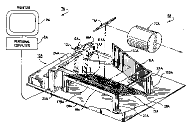
Referring now to FIGS. lA-6A of the drawings, and
more particularly to FIG. lA, there is shown a projection
illumination system 6A which is constructed in accordance
with the present invention, and which is illustrated
20 connected to a video signal producing system 7A including
a personal computer 8A and monitor 9A. The system 6A is
adapted to project computer generated images onto
remotely located viewing surfaces (not shown).
The system 6A generally includes an integrated
25 projector 10A having a base portion or housing 20A,
confining a projection lamp assembly llA including a high
. intensity lamp 13A (as shown in FIG. 2) and a condenser
lens assembly 26A, together with a pair of spaced-apart
finely faceted mirrors 15A and 17A for directing the
30 light from the assembly llA onto a lower light impinging
surface of a horizontal liquid crystal display 24A, which
serves as an image forming display device. Disposed
above the liquid crystal display 24A is a top output
mirror assembly l9A, and a projection lens system or
35 assembly 22A, for facilitating the projection of an image
.
WO95/08132 PCT~S94/10622
21 ~1~6~ --
onto a remote viewing surface (not shown). This is just
one possible orientation of the lens assembly 22A. Other
orientations are possible, such as a vertically directed
orientation.
In order to cause the display panel 24A to modulate
the light from the mirrors 15A and 17A, a display control
system 25A responsive to the personal computer 8A, sends
control signals to the display 24A. The display control
system 25A includes various control logic for
compressing, panning, zooming and controlling the system
images, as more fully described hereinafter.
The li~uid crystal panel 24A is supported by four
legs, such as the leg 27A, enabling the housing 20A to
have a low profile and thus be more compact. The liquid
crystal display panel 24A is more fully described in U.S.
patent application Serial No. 08/237,013 filed on April
29, 1994, which is incorporated herein by reference.
Also, it will become apparent to those skilled in the art
that there are many different transmissive and reflective
spatial modulators or light valves which may be used in
place of the liquid crystal display 24A.
The lamp assembly llA including the condenser lens
assembly 26A is mounted at a rear portion of the housing
20A and provides a source of high intensity projection
light for passing through the liquid crystal display
panel 24A. The finely faceted mirrors, which will be
described hereinafter in greater detail, form part of the
inventive projection illumination arrangement for
directing light from the condenser lens assembly 26A,
through the liquid crystal display panel 24A, to the top
output mirror assembly l9A for projection via the lens
assembly 22A. In this regard, the faceted mirror
arrangement directs the horizontal, forwardly directed
high intensity light within the housing 20A along an
irregularly shaped light path extending from the mirror
WO95/08132 P~S94/10622
21 7 1 ~6 ~
15A perpendicularly to the mirror 17A and then upwardly
through the liquid crystal display panel 24A.
In operation, the projector lOA is positioned on a
stationary surface, such as a table top (not shown) with
a front portion of the housing disposed closest to the
remotely located surface to receive the projected image.
The personal computer 8A, is coupled electrically to the
display panel 24A via the display control system 25A for
enabling computer generated images to be formed by the
display panel 24A.
Light from the condenser lens assembly 26Ais
directed by the faceted mirror arrangement along the
irregularly shaped light path which extends from the
condenser lens assembly 26Ato the mirror 15A and
perpendicularly therefrom to the mirror 17A. From there,
the light is reflected vertically upwardly to the low
light impinging surface of the liquid crystal display
panel 24A to form the desired image. The top output
mirror assembly l9A and the projection lens assembly 22A,
projects reflectively the light image formed by the
display panel 24A onto a viewing surface (not shown).
To effectively greatly reduce or eliminate image
distortion, and to provide a precisely expanded light
beam, the faceted mirror arrangement is disposed between
the light source and the display panel, and the mirrors
are constructed and arranged to reduce image distortion.
By arranging the mirrors 15A and 17A in this manner, the
projection light from the condenser lens assembly 26A can
be precisely directed onto the light impinging surface of
the display panel 24A by adjusting its shape in both the
X and Y dimensions as hereinafter described in greater
detail. Thus, the light is confined in a compact space
to reduce the overall size of the housing 20A.
In order to accomplish the precise directing of the
light, the faceted mirrors spread the light into a set of
WO95/08132 PCT~S94/10622
2 t ~
24
beam segments to form an overall beam of a generally
rectangular cross-sectional configuration, which is
generally similar to the size of the face of the display
panel 24A. For the purpose of filling in any blank or
dark spaces between adjacent beam segments, as
hereinafter described in greater detail, the mirror 15A
is spaced sufficiently from the mirror 17A, which, in
turn, is spaced sufficiently from the display panel 24A
to permit the beam segments to diverge sufficiently to
uniformly cover the bottom face of the display panel 24A
with little or no dark or shadow areas. Thus, the image
is then formed by the display panel 24A in a
substantially undistorted manner within a compact space.
Considering now the lamp assembly llA including the
condenser lens assembly 26A in greater detail with
reference to FIGS. lA and 2A, the assembly llA generally
includes a lamp housing unit 12A which is mounted at the
rear portion of the housing 20A. The lamp housing unit
12A includes a high intensity lamp 13A (FIG. 2A) and a
spherical reflector 14A, both of which direct the light
generated thereby to the condenser lens assembly 26A,
which includes condenser lens elements 2lA, 22A and 23A,
for directing the light toward the first faceted mirror
15A. The three lens elements are nested and curved, and
are progressively larger in size as they are positioned
further from the lamp 13A. It should be understood that
other types and kinds of lamps may also be employed.
The lamp housing unit 12A provides a means for
mounting the condenser lens assembly 26A at a
predetermined distance from the lamp 13A. As indicated
in FIG. 2A, light rays generated by the lamp 13A travel
in a generally parallel manner to the faceted mirror 15A
in a direction perpendicular to the surface of the
condenser lens assembly 26A. However, as hereinafter
described in greater detail, as a practical matter, the
Wo 95108132 PCT/US94/10622
~ 2f7196~
light is spread and is not entirely parallel as indicated
in FIG. 2A. This fact is compensated for according to
the present invention.
- Considering now the faceted mirror arrangement in
5 greater detail with reference to FIGS. lA-3A, the faceted
mirrors 15A and 17A are angularly spaced apart in close
pro~imity to one another. The mirror 15A is vertically
disposed and is positioned with its light impinging face
at an angle to the horizontal collimated light emitted
from the lamp 13A to reflect such light perpendicularly
horizontally toward the mirror 17A.
The faceted mirror 17A is inclined backwardly at an
angle and is supported at its upper edge 17BA by a
U-shaped support frame 18A. The mirror 17A is supported
15 at its lower edge 17AA by an elongated support bracket
28A mounted on the housing 20A. The mirror 17A is
positioned at a sufficient angle to reflect the incident
horizontal beam perpendicularly vertically upwardly
toward the bottom face of the horizontal display panel
20 24A for illuminating it.
The faceted mirrors 15A and 17A have sufficiently
finely spaced facets for segmenting the light being
reflected from their surfaces. The resulting
spaced-apart light beam segments are sufficiently closely
25 spaced to cause them to diverge and fill in any dark or
shadow spaces therebetween, before they impinge upon the
adjacent surface. As hereinafter described in greater
detail, this result is dependent on various factors,
including the redirecting of light beams from the light
30 source, the size of the light source, and the effective
focal length of the condenser lens assembly 26A, for a
given configuration of the angle of the mirror facets,
the spacing of the individual facets, and the distance
between each mirror and its adjacent component, such as
35 the distance between the mirrors 15A and 17A, and the
WO 95/08132 PCT/US94/10622
2 t ~ t
26
distance between the mirror 17A and the display panel
24A.
The mirrors 15A and 17A are each similar to one
another, and thus only the mirror 15A will now be
5 described in greater detail. The vertical mirror 15A
includes a tapered back plate 15BA having on its face a
series of angularly disposed facets, such as the facets
29A and 30A (FIG. lA) projecting angularly outwardly
therefrom. The facets extend vertically between the
bottom edge 15AA and a top edge 15CA.
As best seen in FIG. 4A, the facets, such as facets
37A and 39A, are each generally triangularly shaped in
cross section, and are each similar to one another. The
series of triangularly shaped facets are arranged in a
15 side-by-side arrangement to provide a sawtooth
configuration. Each one of the facets, such as the facet
37A, includes a sloping reflecting surface, such as the
surface 37AA, which is integrally joined at an external
corner edge, such as the edge 37BA, to a right angle
surface 37CA. The reflecting surface serves to reflect
the light from the lamp 13A toward the mirror 17A.
Collimated light from the lamp 13A engages and is
reflected from the angularly disposed reflecting surface,
such as the surface 37AA, between its corner edge 37BA
25 and an adjacent corner edge 39AA of a facet 39A disposed
toward the lamp 13A, to help spread the light beam by
separating it into separate beam segments, such as beam
segments 4 OA and 5 OA .
In order to fill in the dark or shadow areas between
30 the beam segments for reducing image distortion, the
mirrors 15A and 17A are sufficiently spaced apart to
permit the beam segments to diverge and overlap or
intersect before they impinge on the mirror 17A. In this
regard, spaces or gaps between the beam segments are
WO9S/08132 2 ~ 7 ~ ~6 1 PCT~S94/10622
filled in prior to impinging the closest portion of the
- mirror 17A.
The mirrors 15A and 17A are disposed at their
closest portions at their forward portions thereof, as
5 indicated in FIG. 4A at the forward end facets 37A and
39A. In this regard, according to the present invention,
the mirrors 15A and 17A are positioned at their closest
portions by a distance at least equal to a straight line
distance indicated generally at 33A, sufficient to permit
the diverging beam segments 40A and 50A to overlap or
converge together at a vertical line 31A, before engaging
the mirror 17A. The straight line distance 33A extends
normal to the mirror at the vertical line 31A
(illustrated as a point in the plan diagrammatic view of
15 FIG. 4A), and intersects with an internal corner edge 41A
joining integrally the facets 37A and 39A.
The remaining beam segments overlap prior to their
engagement with the mirror 17A. For example, the beam
segment 50A overlaps or intersects with its adjacent beam
20 segment 60A at a vertical line 61A (shown as a point in
FIG. 4A). Such vertical lines 31A and 61A of
intersection are disposed within a vertical plane
generally indicated at 35A as a line, extending generally
parallel to the plane of the back plate 15BA. Thus, all
25 of the remaining beam segments overlap or intersect at
the plane 35A, and thus fill in dark or shadow spaces
prior to their impingement upon the mirror 17A.
It should be understood that a similar relative
spacing between the mirror 17A and the light impinging
30 surface of the display panel 24A to avoid dark or shadow
areas thereon. Thus, a fully illuminated display panel
is achieved, and thus image distortion is eliminated or
at least greatly decreased.
The faceted mirror arrangement acts to spread the
35 light in both the X and Y directions. Light from the
WO95/08132 PCT~S94/10622
6 t
lamp 13A is directed in a manner perpendicular to the
lens assembly 26A surface toward the first faceted mirror
15A. As shown in FIG. 2A, the light is spread and
enlarged in the Y direction as it is reflected from the
finely faceted surface of mirror 15A in a precise manner
to correspond to the Y dimension of the mirror 17A. The
mirror 15A directs these Y direction spread apart light
beam segments toward the second faceted mirror 17A. As
shown in FIG. 2A, the second faceted mirror 17A, then
segments and spreads the light in the X direction
corresponding to the X dimension of the mirror 17A.
Thus, the individual light beams diverge and intersect or
slightly overlap just as they impinge on the surface of
the underside of the liquid crystal display panel 24A.
As a result, the light generated by the lamp 13A, has
been adjusted precisely in the X and Y directions to
provide a compact and effective configuration for the
projection equipment of FIG. lA. Furthermore, since the
faceted mirrors 15A and 17A are arranged in close
proximity to one another, the overall configuration
facilitates the construction of a very compact projector
unit capable of employing a conventional lamp assembly
such as assembly llA to generate high luminosity for
projection illumination purposes in a highly efficient
and effective manner.
Because the light source has a finite extent, the
light rays from lamp 13 are distributed over an angular
range instead of traveling parallel as shown
diagrammatically in FIG. 4A. As a result, the spacing
between the mirrors 15A, 17A and the panel 24A can be
adjusted so that the shadow areas between the beams are
filled in before they impinge on the surface of the panel
24A (FIG. lA). This is very important, as the LCD
display panel 24A is where the image is formed and the
WO95/08132 PCT~S94/10622
~ 211~9~t
presence of the shadow areas here would otherwise cause
image distortion or other undesirable results.
In order to prevent loss of light, the internal
- components of the projector, such as the mirrors 15A and
17A, the LCD panel 24A, the light source and the
condenser lens assembly 26A, should all be positioned as
close together as possible to reduce light loss.
Therefore, for the spacing shown in FIG. 4A between the
two faceted mirrors 15A and 17A, the closest distance is
represented by the line 38A.
The spreading light beams must overlap or converge
together at least within the given shortest distance 38A.
Angle A represents the degree of light spreading.
Angle A is critical, because if angle A were smaller than
as indicated in FIG. 4A, the two adjacent light beams 40A
and 50A would not intersect at point 31A and the second
mirror 17A surface, and therefore there would be a
spacing or shadow area between the two adjacent light
beams. Although not shown in FIG. 4A, the same would be
true regarding the beams reflecting from the second
mirror 17A to the LCD display panel 24A in FIG. lA, when
the light is reflected from the second mirror 17A onto
the LCD panel 24A. Therefore, in accordance with the
invention, the angle A is determined such that the shadow
areas are eliminated, certainly once the reflected light
impinges on the LCD panel 24A of FIG. lA to form properly
the image to be projected.
For this purpose, the angle A is equal to the arc
tangent of the size of the light source 13A, divided by
WO95/08132 PCT~S9~/10622
~ t ~
the effective focal length of the condenser lens assembly
26A. This relationship is expressed as follows:
arlgle of spIeading = A =
arc tan / size of light source
~effective focal length of optical elementJ
where the size of the light source is a dimension that
can be determined by a measurement of a given light
source, and the optical element is the lens assembly 26A .
Therefore, by taking the arc tangent of the size of the
light source, divided by the effective focal length of
the condenser lens assembly, the angle A of the spreading
of the light is determined so that the angles of the
plane of the mirror 15A and its facets can be adjusted to
cause the light beams to overlap at least within the
shortest distance 3 8 as indicated in FIG. 4A .
Referring now to FIG. 5A, there is shown an overhead
projector 6 OA constructed in accordance with the present
invention. The overhead projector 60A is generally
similar to the apparatus of FIGS. lA-3A, except that the
projector 60A is adapted to project images formed by a
transparency (not shown) or the like. The projector 60A
includes a conventional mirror and projection lens
assembly 62A mounted in place by means of a support arm
68A above an image forming display device in the form of
a transparency supporting stage 64A ( in place of the
display panel 24A of FIG. lA). A projection illumination
arrangement 66A is disposed below the stage 64A.
The projection illumination arrangement 66A is
generally similar to the illumination system of FIG. lA,
and includes a high intensity light source 71A, a
collimating lens (not shown), and two angularly disposed
faceted mirrors 73A and 75A. The light emitted by the
light source 71A is collected and directed toward the
vertical faceted mirror 73A by a parabolic reflector (not
shown) or a collimating lens, such as a 3-element
W095/08~32 2 t 7 1 ~6 ~ PCT~S94/10622
condenser lens (not shown). The light is then reflected
from the surface of the vertical faceted mirror 73A
toward the backwardly inclined upwardly faceted mirror
- 75A, and reflected therefrom vertically upwardly through
the stage 64A. The light is segmented and spread in the
X and Y dimensions in a similar manner as described in
connection with the illumination system of FIG. lA. The
spacing between the mirrors 73A and 75A, and between the
mirror 75A and the image forming device 64A are similar
to the illumination arrangement of FIG. lA.
The stage 64Ais positioned between the projector
illumination arrangement 66A and the projection lens
assembly 62A. The stage 64A aids in forming a desired
image by supporting from below transparencies (not
shown), separate liquid crystal display panels (not
shown), or the like.
Referring now to FIG. 6A, there is shown another
form of an overhead projector lOOA, constructed in
accordance with the present invention. The overhead
projector lOOAis generally similar to the apparatus of
FIGS. lA-3A, except that the lamp assembly 103A includes
a high intensity lamp lOlA having a parabolic reflector
107A instead of a condenser lens assembly.
Considering now the lamp assembly 103A in greater
detail with reference to FIG. 6A, the lamp assembly
generally includes a lamp housing unit 105A which is
mounted at the rear portion of the projector housing (not
shown). The lamp housing unit 105A includes a high
intensity lamp lOlA and a parabolic reflector 107A
disposed therebehind, which directs the light generated
thereby toward the first faceted mirror 112A. It should
be understood that other types and kinds of lamps may
also be employed. The parabolic reflector 107A acts to
collect and to redirect forwardly the light emitted by
the high intensity lamp lOlA in such a way that
WO95/08132 PCT~S94/10622
2~ 71 9~1
substantially all light beams are generally parallel. In
this regard, as indicated in FIG. 6A, substantially all
light rays generated by the lamp lOlA travel in a
substantially parallel manner to the faceted mirror 112A,
without the use of a condenser lens.
However, as previously described in connection with
the apparatus of FIG. 4A, the light beam directed from
the parabolic reflector 107A also spreads angularly
outwardly, and therefore, is not precisely parallel as a
practical matter.
As described in connection with the drawing of
FIG. 4A, the angle of spreading of the light beam must be
adjusted in order to eliminate shadow areas between
adjacent light beams being reflected from the faceted
mirror 112A and 114A surfaces for the closest spacing
between the mirror, and between the second mirror and the
LCD panel. It has been determined for the projector lOOA
that the angle of spreading is equal to:
angl e o f spread ing -
~ize of light source
~effective focal len~th of parabolic ~eflectorJ
In this regard, when a parabolic reflector is used, the
spacing or shadow areas between adjacent light beams can
be substantially eliminated by adjusting the size of the
light source or effective focal length of the parabolic
reflector appropriately. Since there is some known
aberration that occurs when a parabolic reflector is
employed, a condenser lens assembly is preferred.
Therefore, it is preferred to use the condenser lens
arrangement 26A as described in the projector of
FIGS. lA, 2A and 3A.
B. THE PROJECTION LENS SYSTEM
Referring now to the FIGS. lB-lOB of the drawings,
and more particularly to FIG. lB thereof, there is shown
a projection lens system or assembly lOB which is
W095/08132 PCT~S94/10622
21~1~6~
constructed in accordance with the present invention.
- The projection lens system lOB is illustrated with a
liquid crystal projector 12B can be employed as the
- projection lens system 22A of FIG. lA, and in accordance
with the method of the present invention can cause a
liquid crystal image to be focused on a remote viewing
surface, such as a remote viewing surface 16B.
The projection lens system lOB generally comprises a
projection lens arrangement 2OB having a Tessar
configuration, variable vertex length and a wide field
coverage angle. The lens arrangement 20B is similar to
lens 22A and is coupled mech~nically to a servo system
22B for adjusting the focal length of the lens
arrangement 20B to cause a projected liquid crystal image
to be focused on the remote viewing surface 16B.
The projection lens arrangement 20B generally
includes three groups G1, G2 and G3 (FIG. lB) of lens
elements arranged along a common optical path P from an
object end ~ to an image end I of the lens arrangement
2OB. The lens arrangement 2OB is disposed between an
object surface Sl via a mirror surface SlA and an image
surface S10. The first group, said second group and said
third group having respective optical powers K1, K2 and
K3, with an overall optical power of about 0.0037 inverse
millimeter. The optical power K1 is about 0.00825
inverse millimeter. The optical power K2 is about -
0.01365 inverse millimeter. The optical power K3 is
about 0.00783 inverse millimeter.
The back focal length between the back vertex of the
lens arrangement 20B and the object surface SlA is about
twelve inches or about 254.6 millimeters. The object
surface SlA is generally rectangular in shape having a
corner to corner diagonal length of about 8.4 inches or
about 106.68 millimeters. Based on the foregoing, those
skilled in the art will understand the effective focal
WO95/08132 PCT~S94/10622
21~t96~ --
34
length of the lens arrangement is between about 10.24
inches or about 260.86 millimeter and about 11.00 inches
or about 280.01 millimeters.
In order to reach full field coverage of the object
with good resolution, the lens arrangement 20B has a
field coverage angle of up to about 22.1 degrees. In
this regard, the resolution of the projection lens
arrangement 20B is about 6 line pairs per millimeter.
The vertex length of the projection lens arrangement
20B is about 1.81 inches or about 46.22 millimeters. The
vertex length is adjustable and has an adjustment range
between a short length of about 1.497 inches or about
38.02 millimeters and a full length of about 1.81 inches
or about 46.22 millimeters. The aperture or speed of the
projection lens arrangement 20B is about f/5.
In order to identify the sequence positioning of
groups Gl, G2 and G3 from the object end ~ to the image
end I, the lens elements are designated in their
sequential position as Ll-L4. Groups Gl and G2 comprise
the inventive projection lens. Lens L4 is a Fresnel
lens. Also, in order to identify the sequence
positioning of the lens element surfaces, the surfaces
are designated in their sequential positions as S2-S9
from the object end ~ to the image end I of the lens
arrangement 20B.
Considering now group G1 in greater detail with
reference to FIG. lB, group Gl is configured in a doublet
arrangement including the lens elements L1 and L2
respectively. Lens elements L1 and L2 cooperate together
to provide positive optical power where lens element L2
counter corrects lens aberrations introduced by lens
element L1.
Considering now lens element Ll in greater detail
with reference to FIG. lB, surface S3 is complementary to
surface S4 of lens element L2 to permit the two lens
WO95/08132 PCT~S94/10622
2 1 7 1 ~6` ~
elements Ll and L2 to be contiguous along their
respective surfaces S3, S4. The radius of curvature of
surface S3 of lens Ll is identical to surface S9 of lens
L4. In this regard, only a single test plate (not shown)
is required to verify the curvature of lens Ll and L4.
Lens Ll and L3 introduce undercorrected spherical
aberration and astigmatism, as well as positive field
curvature.
Considering now lens element L2 in greater detail
with reference to FIG. lB, surface S5 of lens element L2
is generally plano while surface S4 of lens element L2 is
generally concave. As noted earlier, surface S4 is
complementary to surface S3 of lens element Ll. The
function of lens element L2 is to balance the aberration
of lens Ll and L3 by introducing overcorrected spherical
aberration and astigmatism, as well as negative field
curvature.
Considering now group G2 in greater detail with
reference to FIG. lB, group G2 includes a single lens
element L3, having a lens stop LS. Lens element L3 is a
bi-concave element of negative optical power for counter
correcting lens aberration introduced by lens elements Ll
and L2.
Lens element L3 includes two surfaces S6 and S7
respectively, where each of the surfaces S6 and S7 are
generally concave. The distance between surface S7 of
lens element L3 and surface S8 of lens group G3 is
variable.
Considering now group G3 in greater detail with
reference to FIG. lB, group G3 includes a single lens
element L4 of positive optical power. The function of
lens element L4 is to relay the height output from the
projection lens groups Gl and G2.
As best seen in FIG. lB, lens element L4 includes
two surfaces S8 and S9. Lens surface S9 of lens element
W09S/08132 PCT~S94/10622
2 t ~ t
L4 is generally aspheric while surface S8 of lens element
L4 is generally plano. The distance between surface S8
of lens element L4 and surface S7 of lens element L3 is
variable as lens element L4 is mounted movably relative
to lens element L3. In this regard, the servo system 22B
enables the lens element L4 to be moved rectilinearly
along a track 26B by about .313 inches or about 8.20
millimeters.
The lens arrangement 20B preferably has at least two
aspheric surfaces as previously described, such as the
surfaces S2 and S9. As will be made apparent from the
examples that follow in Table IB, the aspherical surfaces
may be defined by the following equation:
X =( ~ + Z (lB)
1 + ~ C2 (K + 1)y2J
where z = ply2 + P2Y4 + P3Y + P~.Y (2B)
Those skilled in the art will understand that X is a
surface sag from the semi-aperture distance y from the
axis or optical path P; that C is the curvature of a lens
surface of the optical axis P equal to the reciprocal of
the radius of the optical axis P; and that K is a conic
constant (cc) or other surface of revolution.
The following example in Tables IB is an exemplary
of the lens arrangement 2OB embodying the present
invention and which is useful primarily for projecting a
full color liquid crystal image color corrected. The
lens arrangement of Table IB has aspheric surfaces
defined by the foregoing aspheric equation. In the
table, the surface radius for each surface, such as
surface S2, is the radius at the optical axis P, Nd is the
index of refraction, and Vd is the Abbe number. Positive
surface radii are struck from the right and negative
Wo95/08~32 217~6`t PCT~S94/10622
radii are struck from the left. The object is to the
left at surface S1 of a liquid crystal display panel 24B.
Table IB
A lens as shown in FIG. lB scaled for a 5.6 foot
5 conjugate; object distance of 1706.00000mm; object height
of -700.000000; and entrance pupil radius of 17.66231.
Lens Surf. Radius Axial Aperture Element
Ele. Desig. (mm) Distance Radius Comp.
No. Between (mm)
Surfaces
(mm)
S1 -17.09756 17.66231K AIR
S2 73.82133 7.50184 26.00000K BAKlC
L1
S3 - 10.27072V 26.00000K AIR
1112.99810
S4 -99.73322 2.69314 24.50000A LF5C
L2
S5 75.04693 8.70928 24.50000 AIR
S6 -274.05990 2.81867 24.50000K KF6C
L3
S7 62.88152 9.99902 24.50000K SK2C
S8 -73.82133 289.33000 24.50000K AIR
L4
S9 - 3.98780 124.71569S ACRYLIC C
..
S10 -46.72718 10.49020 132.00000 AIR
WO95/08132 PCT~S94/10622
21 71 96i
38
Refractive Indices (Nd)
Lens Element RNl/RN4 RN2/RN5 RN3/RN6 VNBR
Element Comp.
AIR ~
L1 BAKIC 1.57250 1.57943 1.56949 57.54848
AIR
L2 LF5C 1.58144 1.59146 1.57723 40.85149
1.59964
AIR
L3 KF6C 1.51742 1.52434 1.51443 52.19566
1.52984
L4 SK2C 1.60738 1.61486 1.60414 56.65632
1.62073 - - -
AIR
ACRYLIC 1.49177 1.49799 1.48901 56.01934
1.50377
AIR
Aspheric parameters of L4 (S9)
CC -1.01435
P1 0.00711
P2 -2.6576 x 10⁻⁸
P3 4.1592 x 10⁻¹⁴
P4 1.5503 x 10⁻¹⁷
Referring now to FIGS. 2AB-2CB there is illustrated
the ray displacement caused by the lens arrangement 2OB.
FIG. 2AB illustrates ray displacement where the FOB is
about 1.0 and a 5.6 foot conjugate. In this regard, a
pair of displacement curves 302B and 303B illustrates the
ray displacement when the image wavelength is about 0.588
microns. Other pairs of ray displacement curves are
illustrated for different image wavelengths such as a
pair of displacement curves 304B and 305B illustrate the
ray displacement when the image wavelength is about 0.486
microns; a pair of displacement curves 306B and 307B
illustrate the ray displacement when the image wavelength
is about 0.656 microns; and a pair of displacement curves
WO95/08132 PCT~S94/10622
~ 217~9~1
308B and 309B illustrate the ray displacement when the
- image wavelength is about 0.436 microns.
FIG. 2BB is similar to FIG. 2AB except the FOB is
about 0.7. The pairs of ray displacement curves for
wavelengths of 0.588; 0.486; 0.656; and 0.436 are
312B,313B; 314B,315B; 316B,317B; and 318B,319B,
respectively.
FIG. 2CB is similar to FIGS. 2AB and 2BB except the
FOB is about 0Ø The pairs of ray displacement curves
for wavelengths of 0.588; 0.486; 09.656; and 0.436 are
322B,323B; 324B,325B; 326B,327B; and 328B,329B
respectively.
FIGS. 3AB-3CB and 4AB-4CB are similar to FIGS. 2AB-
2CB and illustrate pairs of displacement curves for
wavelengths of 0.588; 0.486; 0.656 and 0.436 relative to
different FOB of 1.0, 0.7 and 0 respectively. In order
to identify curve pairs in FIGS. 3AB-3CB and 4AB-4CB as
described in FIGS. 2AB-2CB the first character reference
number identifying the curves in FIGS. 3AB-3CB and 4AB-
4CB have been sequentially increased. For example, acurve pair 402B and 403B correspond in description to the
curve pair 302B and 303B. Based on the foregoing, no
further description will be provided for the 4.0 fast
conjugate curves 402B-409B; 412B-429B; 422B-429B; and the
10.0 foot conjugate curves 502B-509B; 512B-519B; and
522B-529B.
Referring now to FIGS. 5AB-5CB; FIGS. 6AB-6CB and
FIG. 7AB-7CB there is illustratéd astigmatism, distortion
and lateral color curves for the lens arrangement
examples having the 4.0 foot conjugate, 5.6 foot
conjugate and 10 foot conjugate respectively. The
respective astigmatism, distortion and lateral color
curves are identified as 601B; 602B; 603B; 604B and 605B
for the 4.0 foot conjugate, 701B; 702B; 703B; 704B and
WO95108132 PCT~S94/10622
2~t~61 ~
705B for the 5.6 foot conjugate, and 801B; 802B; 803B;
804B and 805B for the 10.0 foot conjugate.
Referring now to FIG. 8B there is illustrated a
series of modulation transfer function curves 901B-905B
of the lens arrangement example having the 4.0 foot
conjugate. Each curve depicted illustrates the
modulation as a function of frequency (cycles per
millimeter).
FIGS. 9B and 10B are similar to FIG. 8B and
illustrate a series of modulation transfer function
curves 1001B-1005B and 1100B-1105B respective for the
lens arrangement examples having 5.6 and 10.0 foot
conjugates respectively.
C. THE DISPLAY CONTROL 8YSTEM COMPRES8ION MODE OF
OPERATION
Referring now to FIGS. lC-8C of the drawings, and
more particularly to FIG. lC thereof, there is shown a
display control system 10C which is constructed in
accordance with the present invention. The display
control system 10C can be employed as the display control
system 25A of FIG. lA, and is illustrated coupled between
a video signal producing device, such as a video output
module 12C of a personal computer 14C and a display
device, such as a liquid crystal display unit or panel
16C for displaying a compressed image defined by a matrix
array of pixel images arranged in n number of rows and m
number of columns. In this regard, the number n is about
1024 and the number m is about 768.
The display control system 10C generally includes a
low speed sampling circuit 20C that converts an incoming
analog RGB video data signal 18C, developed by the output
module 12C, into a pixel data signal 21C for helping a
compressed image to be displayed by the liquid crystal
display unit 16C in a cost effective manner. In this
regard, as will be explained hereinafter, the sampling
WO95/08132 PCT~S94110622
~ ~171q6~
41
circuit 20C includes a low cost, low speed, analog to
digital converter arrangement that has a sampling rate
which is substantially slower than the incoming rate of
the video data signal which is typically between about 15
MHz and about 135 MHz.
A timing circuit 22C develops various timing signals
that enable the sampling circuit 20C to receive and
convert the incoming video data signal into pixel data
2lC that is indicative of a workstation image or image to
be compressed defined by a matrix array of pixel images
arrayed in N number of rows and M number of columns. In
this regard, the number N is about 1280 and the number M
is about 1024. As the sampling rate of the sampling
circuit 20C is substantially slower than the incoming
data rate of the video data signal 18C, it should be
understood by those skilled in the art that during any
given frame time period, only one-half of the pixel image
information for any frame cycle is converted into pixel
data. Thus, the whole workstation image is converted
into pixel data once every two frame cycle periods.
The display control system 10C also includes a
programmable logic device or state machine 24C which is
responsive to the timing circuit 22C for generating
addressing or compression signals to help compress the
whole workstation image on the fly into a compressed
image that is displayed by the liquid crystal display
unit 16C. The state machine 24C is driven by frame
signals indicative of ODD frame time periods and EVEN
frame time periods. One such state machine 24C was
constructed using GAL logic. The actual program design
of the GAL logic is shown in Appendix AC.
The system 10C also includes a data output circuit
26C responsive to the timing logic circuit 22C and the
programmable logic device 24C for causing only certain
,
WO95/08132 PcT~S94/10622
2? ~61
42
portions of the pixel data 21C to be gated to the liquid
crystal display panel 16C each frame.
In operation, the sampling circuit 20C converts the
incoming video data signal 18C based upon whether a given
frame cycle is an odd frame time period or cycle or an
even frame time period or cycle and whether the video
data signal being sampled is indicative of an odd pixel
image in the M by N pixel image array or an even pixel
image in the M by N pixel image array. More
particularly, the sampling circuit 20C converts the video
data signal indicative of odd pixel images on odd lines
in the M by N matrix array and even pixel images on even
lines for every even frame time period. Alternately, for
every odd frame time period, the sampling circuit 20C
converts the video data signal indicative of even pixel
images on odd lines in the M by N matrix array and odd
pixel images on even lines. In this manner, every analog
pixel image signal embodied within the workstation-based
image is converted into pixel data once every two frame
time periods.
From the foregoing, it should be understood by those
skilled in the art, that causing the whole workstation
image to be converted once every two frame time periods
results in a substantially flicker free image being
displayed by the liquid crystal display unit 16C.
The compression technique of the programmable logic
device 24C also alternates between odd frame time periods
and even frame time periods. In this regard, the device
24C causes designated pairs of pixel image columns and
designated pairs of pixel images within each rows to be
averaged over every two frame cycle periods to produce a
series of averaged or single pixel image columns and a
series of averaged pixel image pairs. The averaged pixel
image columns are indicative of a single pixel image
WO95108132 PCT~S94/10622
~ 217196~
43
column. The averaged pixel image pairs are indicative of
a single pixel image.
The above described compression technique does not
involve composite pixel arrangements, nor expensive
buffer memory devices. Instead, conversion of the
incoming video data signal 18C into a compressed image is
accomplished on the fly in a relatively inexpensive
manner with simple buffer logic and low speed analog to
digital converters.
Considering now the sampling circuit 20C in greater
detail with reference to FIG. 3C, the sampling circuit
20C includes a set of analog to digital converter
arrangement 31C for converting the incoming analog red,
green and blue video module signals into digital signals.
A sample clock signal 34C generated by a logic gating
arrangement 36C, enables the incoming analog signals to
be converted at a predefined rate that allows only odd
pixel image data to be converted during odd line, odd
frame time periods and odd line, even frame time periods
and only even pixel image data to be converted during
even line, odd frame time periods and odd line, even
frame time periods. In this manner, the image to be
compressed, is sampled or converted on the fly at a rate
that is substantially slower than the incoming data rate.
As will be explained herein in greater detail,
during each odd frame time period, one half of the image
to be compressed is converted and during each even frame
time period, another half of the image to be compressed
is converted. In this manner, conversion of the image is
averaged over the entire image.
Referring now to FIGS. 5C and 6C, the conversion of
the M by N matrix image data is illustrated
diagrammatically in greater detail. In FIG. 5C, each
circled pixel image element, such as an element 501C and
an element 502C is indicative of a converted incoming
WO95/08132 PCT~S94/10622
2~7t~6t ~
analog signal during an odd frame time period. Thus, in
odd lines such as lines 1, 3, 5, . . . 1023, odd pixel
image data has been converted and in even lines, such as
lines 2, 4, 6, . . . 1024 even pixel image data has been
converted.
FIG. 6C illustrates the conversion of the M by N
matrix image data diagrammatically. In this regard, each
circled pixel image element such as an element 503C and
an element 504C is indicative of the converted incoming
analog signals during an even frame time period. More
particularly, as best seen in FIG. 6C, during odd lines,
even pixel image data has been converted and during even
lines, odd pixel image data has been converted.
Because of the slow response time of the liquid
crystal panel 16C, the image formed by the panel 16C
during the odd frame time period is combined with the
image formed by the panel 16C during the even frame time
period to be perceived by a viewer as a whole image in a
substantially flicker free manner.
Considering now the gating arrangement 36C in
greater detail, the gating arrangement 36C generally
includes a set of logic gates 101C-105C which implements
the function of determining which pixel data is to be
sampled or converted. In this regard, depending on the
odd/even frame cycle, and whether image data is to be
displayed on an odd/even line, a clock signal lloC will
be passed by one of the gates 101C-104C to a logic OR
gate 105C to cause the sample clock signal 34C to be
generated.
Considering now the programmable logic device 24C in
greater detail with reference to FIG. 2C, the device 24C
generally includes a group of logic circuits 1000C-1512C
and a multiplexor arrangement 42C for generating a line
address or compression signal for causing the vertical
portion of the image to be compressed from N lines to n
wo9s/08132 2 t 7 1 ~ 6- 1 PCT~S94/10622
lines. In a preferred form of the invention, the logic
circuits lOOOC-1512C are embodied in gate array logic,
and are shown in Appendix AC. The preferred language is
ALTERA's Advanced Hardware Descriptive Language (AHDL).
The logic circuits lOOOC-1512C are arranged to cause
certain lines or rows of pixel image data in the
workstation-based image to be eliminated every odd frame
cycle. During every even frame cycle, certain other
lines or rows of pixel image data are eliminated. The
two sets of eliminated lines or rows are thus averaged
together to cause the number of lines to be compressed
from N lines to n lines. As will be explained
hereinafter, since the liquid crystal display panel 16C
has a slow response time, the compressed image is
indicative of and perceived by the viewer as the entire
workstation image as each line in the workstation image
is in fact displayed once every two frame cycles.
Referring now to FIGS. 7C and 8C, the averaging of
lines of pixel image data is illustrated diagrammatically
in greater detail. In FIG. 7C, during an odd frame time
cycle, every third out of four rows or lines of pixel
image data is eliminated such as a row 703C, 707C and
711C. Thus, lines 3, 7, 11, etc. are eliminated. In
FIG. 8C, during the even frame cycle, every fourth out of
four rows or lines of pixel image data is eliminated such
as a row 704C and 708C. Thus, lines 4, 8, 12 etc. are
eliminated. As the eliminated third and fourth line
groups, such as line 3C and line 4C are adjacent to one
another, the viewer perceives the resulting image as a
combination of both the eliminated lines. Because the
entire workstation-based image is actually displayed
every two frame cycles, the resulting image is displayed
without introducing any substantial stripping.
In order to enable adjacent lines of pixel images to
be averaged, the multiplexor arrangement 42C generally
WO95/08132 PCT~S94110622
._
2 1 7 1 ~
46
includes a plurality of groups of line address pair
circuits. In this regard for example, the odd frame time
logic for gating lines l, 2, 3 is multiplexed with the
even frame time logic for gating lines l, 2, 4 to permit
lines 3 and 4 to be averaged.
From the foregoing, it will be understood by those
skilled in the art that the multiplexor arrangement 42C
includes a plurality of line address drivers (not shown)
which are coupled to data output logic 26C by an address
buss line 29C.
Considering now the data output logic 26C in greater
detail with reference to FIG. 2C, the data output logic
26C generally includes a set 50C of frame buffer devices
coupled to the address buss line 29C and a set 52C of
multiplexors for assembling output data in odd and even
byte pairs. The set 50C of frame buffer devices are
responsive to pixel data converted by the sampling
circuit 20C as well as the line address signals generated
by the programmable logic device 24C. In this regard,
the set 50C of frame buffer devices enables certain
adjacent columns of pixel image data to be averaged
together over every two frame cycles to form sets of
single pixel image columns.
Considering now the set 50C of frame buffer devices
in greater detail, the set 50C of devices generally
includes a group of logic circuits 60C-64C for generating
compression signals 70C-73C for causing the horizontal
portion of the image to be compressed from M lines to m
lines. The logic circuits 60C-64C are embedded in the
previously mentioned GAL and are shown in Appendix AC.
The logic circuits 60C-64C are arranged to cause
certain columns of pixel image data in the workstation
image to be eliminated during every odd frame cycle and
certain other columns of pixel image data to be
eliminated during every even frame cycle. The two sets
WO95/08132 PCT~S94/10622
~ 2~ 71 961
47
of eliminated columns are thus averaged together, to
- cause the number of columns to be compressed from M
columns to m columns.
Referring now to FIGS. 7C and 8C, the averaging of
columns of pixel image data is illustrated in greater
detail. In FIG. 7C, during an odd frame time cycle,
every four out of five columns of pixel image data is
eliminated. Thus, columns 4, 9, 14 etc. are eliminated.
In FIG. 8C, during the even frame time cycle, every fifth
out of five columns of pixel image data is eliminated.
Thus, columns 5, 10, 15 etc. are eliminated. As the
eliminated column groups, such as columns 4 and 5 in the
first group and columns 9 and 10 in the second group are
adjacent to one another, the viewer perceives the
resulting image as a combination of both columns (4 and
5) and (9 and 10) for example. Because the entire
workstation image is displayed every two frame cycles,
the resulting image is displayed flicker free and without
introducing any substantial stripping.
Considering now the set 52C of multiplexors, the set
52C generally includes a pair of devices for sending odd
and even pixel data information to the liquid crystal
display unit 16C. In this regard, the set 52C of
multiplexor devices includes an odd multiplexor device
80C and an even multiplexor device 82C. The odd
multiplexor device 80C is coupled to the output of the
logic circuits 60C and 62C. The even multiplexor device
82C is coupled to the output of the logic circuits 63C
and 64C.
Considering now the logic circuits 60C-64C in
greater detail with reference to FIG. 5C, the logic
circuits 60C-64C control compression for the columns
indicated in Table IC.
WO95/08132 PCT~S94/10622
2~7t~61
48
Table IC
Logic Circuit Columns Controlled by Logic Circuit
Character Reference
Pl (60C) 1, 6, 11, 16, 21,..... , 2044
5 P2 (61C) 2, 7, 12, 17, 22,..... , 2045
P3 (62C) 3, 8, 13, 18, 23,..... , 2046
P4 (63C) 4, 9, 14, 19, 24,..... , 2047
P5 (64C) 5, 10, 15, 20, 25,.... ., 2048
From Table IC, it will be understood by those
skilled in the art that column pixel image data
controlled by logic circuits 63C and 64Cwill be
compressed.
As best seen in FIG. 5C, in order to control column
compression the output drivers of logic circuits 63C and
64C are enabled by a pair of logic signals, an ODD FRAME
signal 220C and an EVEN FRAME signal 222C. Logic signal
220C and 222C are generated by the timing logic circuit
22C and are indicative of an ODD frame time period and an
EVEN frame time period respectively. The logic circuits
for generating the ODD FRAME signal 220C and the EVEN
FRAME signal 222C are conventional flip flops (not shown)
and will not be described herein.
When the ODD logic signal 220C is a logical high,
column driver 64C is disabled and column driver 63Cis
enabled. Similarly, when the EVEN logic signal 222C is a
logical high, column driver 63C is disabled and column
driver 64Cis enabled.
The output signals from drivers 63C and 64C are
connected together at a common node N and are coupled to
the multiplexor 82C.
Considering now the timing circuit 22C in greater
detail, the timing circuit 22C generally includes a phase
VCO or pixel clock generator 200C for generating a
reference or pixel clock signal 202C and a pair of
WO95/0~132 2 1 7 1 ~6 1 PCT~S94/10622
unsynchronized clock generators, such as an odd clock
generator 204C and an even clock generator 206C for
generating a CLKA signal 205C and CLKB signal 207C
respectively. A phase lock loop 201C causes the signals
205C and 207C to be synchronized relative to one another
as best seen in FIG. 4C.
A logic arrangement 208C consisting of a set of
logic gates 210C-212C coupled to the clock generators
204C and 206C develop an output CLOCK signal 214C. The
clock signal 214C is phase shifted once each frame cycle
to enable odd pixel data to be sampled during one frame
cycle period and even pixel data to be sampled during the
next frame cycle period.
The timing circuit also includes a group of logic
elements (not shown) that generate an ODD line signal
221C and an EVEN line signal 223C. Those skilled in the
art would be able to arrange logic elements to determine
whether a given line was an odd line or an even line
without undue experimentation.
D. THE DIæPIlAY CONTROI. SYSTEN PANNING MODE OF OPERATION
Referring now to FIGS. lD-13D of the drawings, and
more particularly to FIG. lD thereof, there is shown a
display control system 10D which is constructed in
accordance with the present invention. The display
control system 10D can be employed as the display control
system 25A of FIG. lA, and is illustrated connected to a
personal computer 12D, having a video control module (not
shown) for driving a workstation monitor 14D and a liquid
crystal display monitor 16D simultaneously. The display
control system 10D, in accordance with the method of the
present invention, can rewrite the video information from
the personal computer 12D to both the workstation monitor
14D having an M by N or 1280 x 1024 pixel element matrix
array and the liquid crystal display unit 16D having an m
by n 1024 x 768 pixel element matrix array
WO 95/08132 PCT/US94/10622
2~7~61
simultaneously. In this regard, as more fully disclosed
herein, the display control system lOD compresses a
workstation video image 14AD displayed on the workstation
monitor 14D in such a manner so that substantially the
entire 1280 x 1024 workstation image is displayed as a
1024 x 768 liquid crystal display image 16AD by the
liquid crystal display panel 16D. The display control
system lOD can control the liquid crystal display unit
16D to enable the workstation image 14AD to be panned in
accordance with the method of the present invention.
The display control system lOD generally includes a
control circuit 20D that controls the sampling of an
incoming analog RGB video data signal 15D, developed by
the video control module in the personal computer 12D.
In this regard, the control circuit 20D causes only a
selected portion of the incoming video data signal 15D to
be sampled and converted into digital data by an analog
to digital converter 18D. A control gate 34D under the
control of the control circuit 20D, passes an A/D clock
signal 36D that enables the analog to digital converter
18D to sample the incoming video data signal 15D for
conversion purposes. As will be explained hereinafter,
the A/D clock signal 36D is synchronized with the
incoming video data signal 15D via a pixel clock signal
32D.
A video data buffer RAM memory unit l9D coupled to
the digital converter 18D by means not shown, stores the
selected and converted portion of the video information,
where the selected portion is indicative of a 1024 x 768
portion of 1280 x 1024 workstation video image. As will
be explained hereinafter, a user employing a remote
control panning device 22D can select any 1024 x 768
portion of the 1280 x 1024 workstation image to be
displayed on the liquid crystal display panel 16D.
WO95/08132 PCT~S94/10622
2-171~61
A microprocessor 24D coupled to the remote control
- panning device 22D via an infrared receiver 23D, causes
the displayed portion of the workstation image to be
changed in response to input command signals generated by
the device 22D.
A voltage controlled oscillator circuit or pixel
clock generator 30D, synchronized by an HSYNC signal 17D
develops the pixel clock signal 32D for synchronizing the
A/D clock signal 36D with the incoming video data signal
15D.
In operation, as best seen in FIGS. 2D-7D, whenever
a user desires to pan the workstation image 16AD
displayed on the li~uid crystal display panel 16D, the
user, via the remote control panning device 22D, causes a
panning command signal to be transmitted to the
microprocessor 24D. In response to receiving the panning
control signal, the microprocessor 24D, via the control
circuit 20D, causes the workstation image 16AD displayed
on the liquid crystal display panel 16D to be changed.
In this regard, only a central portion lOOD (FIG. lOD) of
the workstation image 14AD is displayed, where the
central portion lOOD is defined by a 1024 x 768 matrix
array of pixel images indicative of lines 129 to 896 of
the workstation image 14AD and columns 129 to 1152 of the
workstation image 14AD.
After the central portion lOOD is displayed, the
user, via the remote control panning device 22D, can
cause pan left, right, up and down signals to be
transmitted to the microprocessor 24D to view different
portions of the workstation image.
In response to each pan left signal received by the
microprocessor 24D, the control circuit 20D causes the
displayed image to be changed column by column to a left
central portion 102D of the workstation image 14AD, where
the left portion 102D is defined by a 1024 x 768 matrix
WO95/08132 PCT~S94/10622
2 1 7i q6 1 '
array of pixel images indicative of lines 129 to 896 of
the workstation image 14AD and columns (129-X~) to (1152-
XL)~ where X~ is a whole number integer between 1 and 128.
From the foregoing, it will be understood by those
skilled in the art that when the user pans the LCD image
to a full left position, the left central portion 102D is
defined by a 1024 x 768 matrix array of pixel images
indicative of lines 129 to 896 of the workstation image
14A and columns 1 to 1024 of the workstation image 14AD.
In a similar manner, in response to each pan right
signal received by the microprocessor 24D, the control
circuit 2 OD causes the displayed image to be changed to a
right central portion 104D of the workstation image,
where the right portion 104D is defined by a 1024 x 768
matrix array of pixel images indicative of lines 129 to
896 of the workstation image and columns ( 129 + XR) to
(1152 + XR), where XR is a whole number integer between 1
and 128.
Thus, when the user pans the image to a full right
20 portion, the right central portion 104D is defined by a
1024 x 768 matrix array of pixel images indicative of
lines 129 to 896 of the workstation image 14AD and
columns 256 to 1280 of the workstation image 14AD.
In response to each pan up signal received by the
25 microprocessor 24D, the control circuit 20D causes the
displayed image to be changed to an upper central portion
106D of the workstation image, where the upper portion is
defined by a 1024 x 768 matrix array of pixel images
indicative of lines (129 _ Yu) to (896 _ Yu) ~ where Yu is
30 a whole number integer between 1 and 128.
When the image is panned to a full upper position,
the upper central portion 106D is defined by a 1024 x 768
matrix array of pixel images indicative of lines 1 to 768
of the workstation image 14AD and columns 129 to 1152 of
35 the workstation image 14AD.
W095/08132 PCT/US94/10622
~ 2~7~ti
53
In a similar manner, in response to each pan down
b signal received by the microprocessor 24D, the control
circuit 2 OD causes the displayed image to be changed to a
lower central portion 108D of the workstation image 14AD,
S where the lower portion 108D is defined by a 1024 x 768
matrix array of pixel images indicative of lines
(129 + YD) to (896 + YD), where YD is a whole number
integer between 1 and 128.
Thus, when the user pans the displayed image to a
full lower position, the lower portion 108D is defined by
a 1024 x 768 matrix array of pixel images indicative of
lines 258 to 1024 of the workstation image 14AD.
While in the preferred embodiment of the present
invention the displayed image was defined by a 1024 x 768
matrix array of pixel images, those skilled in the art
will understand other matrix arrays of different sizes
are contemplated within the scope of the invention.
Considering now the display control system lOD in
greater detail, the control circuit 2 OD generally
comprises a line control arrangement 40D and a column or
pixel control arrangement 50D. The line control
arrangement 40D determines which lines, in lines 1 to
1024 of the workstation image, will be displayed by
liquid crystal display 16D. In a similar manner, the
pixel control arrangement 50D determines which columns,
in columns 1 to 1280 of the workstation image, will be
displayed by the liquid crystal display 16D.
Considering now the line control arrangement 40D in
greater detail with reference to FIG. lD, the line
control arrangement 40D generally includes a line hold
off counter 42D and an active line counter 44D and a pair
of decrement gates 43D, 45D which couple decrement pulses
to each of the counters 42D and 44D respectively. The
line hold off counter 42D, is synchronized with the
incoming video data signal 15D via a VSYNC signal 16D
WO~5108132 PCT~S94/10622
2171~
54
generated by the video module in the personal computer
12D. In this regard, the line hold off counter is v
enabled by a VSYNC signal 17AD generated by the personal
computer 12D.
The line hold off counter 42D counts a predetermined
Y number of display lines, following the VSYNC signal
17AD, to be inhibited from display. In this regard, the
microprocessor 24D, upon receiving the pan command
signal, causes the line hold off counter 42D to be loaded
with an initialize Y count via a load signal bus 26D.
The Y count e~uals the number of lines the workstation
image can be panned either up or down. In this regard, Y
can be between a minimum number and a maximum number of
lines capable of being panned up or down depending on the
size of the screen. More particularly, Y is defined by
equation (lD) that follows:
Y = Number of lines inclusive of VS~NC pulses
~ VS~NC blanking interval (1)D
+ Starting line number of the image
The following examples will illustrate the
application of equation (lD):
Screen Location :Equation Application
tY)
0 Upper Left Quadrant Portion Y = VSYNC pulses + VSYNC
blanking + 0
Lower Left Quadrant Portion Y = VSYNC pulses + VSYNC
blanking + 256
Vertically Centralized Y = VSYNC pulses + VSYNC
Portion blanking + 128
From the foregoing, it should be understood that the
initialized value of Y depends upon both the screen size
and the starting line number of the image. Thus, for
example, to start from a center screen position with a
Wos~/08~32 2 1 ~ 1 9 6 1 PCT~S94/10622
.
screen size of 1024x768 pixels, Y will be initialized
- to a value of 128 plus VSYNC pulses plus VSYNC blanking.
In operation, when the VSYNC signal 17AD goes high
at the end of a previous frame time period, the line hold
off counter 42Dis enabled causing its output to a logic
LOW level disabling the active line counter 44D and the
pixel control arrangement 50D. The line off counter 42D
is then loaded with the initialize count of 128, which
count is decremented once each time the HSYNC signal 17D
goes to a logic HIGH level. When the line hold off
counter 42D is decremented to zero, a terminal count
signal 46D is generated which in turn, enables both the
active line counter 44D, and the pixel control
arrangement 50D as will be explained hereinafter in
lS greater detail.
When the active line counter 44Dis enabled, it is
decrement once for each occurrence of the HSYNC signal
17D after the terminal count signal 46D rises to a logic
HIGH level.
The active line counter 44Dis initialized by the
microprocessor 24D, via the load signal bus 26D, with a
predetermined M number, where M is indicative of the
total number of matrix display lines available on the
liquid crystal display unit 16D. In this regard, the
counter44Dis loaded with the number 768 via the load
signal bus 26D.
When the active line counter 44Dis decremented to
zero, it generates a disable signal 47D, which in turn,
causes both disable gates 43D and 45D to be disabled.
The microprocessor 24Dis responsive to both the
VSYNC signal 17AD and the HSYNC signal 17D as well as the
various pan commands transmitted by the user via the
remote control device 22D. In this regard, the
microprocessor 24D includes a conventional algorithm for
determining the current position of the panel image
WO95/08132 PCT~S94~10622
2 1 7 1 q~ 1 --
S6
relative to the corresponding workstation image. Based
on this determination the microprocessor 24D causes the
line control circuit 40D and the pixel control circuit
50D to be loaded with appropriate counts for inhibiting
and enabling display of the user selected portion of the
workstation image.
Considering now the pixel control arrangement 50D in
greater detail, with reference to FIG. lD, the pixel
control arrangement generally includes a pixel hold off
counter 52D and an active pixel counter 54D. The pixel
hold off counter 52D is synchronized with the incoming
analog video data signal 15D via the line hold off
counter terminal count signal 46D and the pixel clock
signal 32D.
When the terminal count signal 46D goes to a logic
HIGH level, the pixel hold off counter 52D is enabled.
In this regard, the counter 52D is initialized by the
microprocessor 24D which causes the counter 52D to be
loaded with an initialize X count via the load signal bus
26D. The X count equals the number of columns the
workstation image can be panned either left or right. In
this regard, X can be between a minimum number and a
~;rum number of columns capable of being panned either
to the left or to the right depending on the size of the
screen. More particularly, X is defined by equation (2D)
that follows:
X = Number of pixels inclusive of HSYNC pulses
+ HSYNC bl anking in terval ~ 2 ) D
+ Starting pixel column number of the image
The following examples will illustrate the
application of equation (2D):
wosslo8l32 2 1 ~ ~ 9 6 t PCT~S94/10622
S7
Screen Location ~ E~uation Application
~:: : : ( X )
Upper Left Quadrant Portion X = HSYNC pulses + HSYNC
blanking interval + O
Upper Right Quadrant X = HSYNC pulses + HSYNC
Portion blanking interval + 256
Horizontally Centralized X = HSYNC pulses + HSYNC
Portion blanking + 128
From the foregoing, it should be understood that the
initialized value of X depends upon both the screen size
and the starting pixel column number within the panned
10 image. Thus, for example, to start from a center screen
position with a screen size of 1024 by 768 pixels, X will
be initialized to a value of 128 plus HSYNC pulses plus
HSYNC blanking.
When the pixel hold off counter 52D is enabled, it
15 is decrement once for each occurrence of the pixel clock
signal 32D. Thus, the output of the pixel hold off
counter 52D will remain at a logic LOW level for 128
pixel clocks. When the pixel hold off counter 52D is
decremented to zero, its output generates a start
20 sampling signal 56D, goes to a logic HIGH level which in
turn, enables both the active pixel counter 54D and the
A/D clock gate 34D.
When the active pixel counter 54D is enabled, it is
decremented once for each occurrence of the pixel clock
25 signal 32D.
The active pixel counter 54D is initialized by the
L microprocessor 24D, via the load signal bus 26D with a
predetermined N number, where N is indicative of the
total number of matrix display columns available on the
30 liquid crystal display unit 16D. In this regard, the
counter 54D is loaded with the number 1024 via the load
signal bus 26D.
WO95/08132 PCT~S94/10622
~ s
'171961
58
When the active pixel counter 54D is enabled, it is
decremented once for each occurrence of the pixel clock
signal 32D. In this regard, when the counter 54D is
decremented to a zero count, it generates a stop sampling
5 signal 57D which in turn, causes the A/D clock gate 34D
to be disabled.
From the foregoing, it will be understood by those
skilled in the art that the A/D clock gate 34D is enabled
only during that time period the pixel hold off counter
start sampling sinal 56D is at a logic HIGH level.
Considering now the remote device 22 D in greater
detail with reference to FIG. 12D, the remote device 22D
generally includes a pan command key 302D which, when
actuated cause a pan command to be sent to the
microprocessor 24D. In this regard, the control circuit
will cause the compressed image 16AD as illustrated in
FIG. 3D to be changed to a central pan image lOOD
(FIG. lOD) upon receipt of the pan command.
The remote device 22D also includes a group 304D of
panning keys that includes a pan left key 310D, a pan
right key 311D, a pan up key 312D, and a pan down key
313D. In operation, by actuating the keys 310D-311D any
panning position as illustrated in FIGS. 3D-llD can be
achieved. In this regard for example, an upper left pan
position llOD, an upper right pan position lllD, a lower
left pan position 112D, and a lower right pan position
113D can be viewed as best seen in FIGS. 8D-9D and llD-
12D respectively.
By way of example, initialized values for X and Y
with a screen size of 1024 by 768 pixels was specified
for a centralized portion of the image to be panned. It
will be understood by those skilled in the art that other
initialized values of X and Y will result for different
screen sizes. Thus, X and Y will be different for screen
sizes of 1152 by 900 pixels, and the like.
W095/08132 PCT~S94/10622
21 7~
B. THE DI~PLAY CONTROL ~S~ l 200MING MODE OF OPERATION
Referring now to FIGS. lE-llE of the drawings, and
more particularly to FIG. lE thereof, there is shown a
display control system lOE which is constructed in
accordance with the present invention. The display
control system lOE can be employed as the display control
system 25A of FIG. lA and is illustrated coupled between
a video signal producing device, such as a personal
computer 12E having a monitor 13E, and a display device,
such as a liquid crystal display unit 15E. While the
preferred embodiment of the present invention describes
the use of a personal computer 12E, it will be understood
by one skilled in the art that other devices including
both high and low resolution devices will also perform
satisfactorily.
The liquid crystal display unit 15E includes a
liquid crystal panel 16E (FIGS. lE-3E) having a 1024 x
768 matrix array of pixel elements for displaying a
monitor image 18E. In this regard, the monitor image 18
can be either a virtually duplicated image 30E (FIG. 2E)
of a personal computer monitor image 14E, or a zoomed
image 31E (FIG. 3E) of the personal computer monitor
image 14E. The duplicated image 30E is defined by a
matrix array of pixel images arranged in n number of rows
and m number of columns, while the zoomed image 31E is
defined by a matrix array of pixel elements arranged in N
numbers of rows and M number of columns. In this regard,
the numbers m and M are about 640 and 1024 respectively,
while the numbers n and N are about 480 and 720
respectively.
From the foregoing, those skilled in the art will
understand the display system lOE enables a user (not
shown) to view an image from the liquid crystal display
panel 16E as either a virtually duplicated image of the
computer monitor image 14E arranged in a matrix array of
Wo 95/08132 I'CT/US94/10622
.
2~71~6
640 x 480 pixels, such as image 30E, or as the
corresponding zoomed image 3 lE arranged in a matrix array
of 1024 x 720 pixels.
The display control system lOE generally includes a
low speed sampling arrangement indicated generally at 20E
that helps convert an incoming analog RGB video data
signal ll9E developed by the personal computer 12E into a
pixel data signal 21AE that is indicative of the 640 x
480 monitor image 14E. In this regard, as will be
explained hereinafter, the sampling arrangement 20E
includes a low cost, low speed analog to digital
converter arrangement indicated generally at 21E that has
a sampling rate which is sufficient to sample all of
incoming video data indicative of the 640 x 480 computer
image at least once each frame time period.
The low speed sampling arrangement 20E also includes
a timing control circuit 22E to develop various timing
signals that enable the analog to digital converter
arrangement 2 lE to convert the incoming video data signal
20 ll9E into pixel data 21AE arranged in a proper format for
display on the panel 16E. From the foregoing, it should
be understood by those skilled in the art that during any
given frame time period, all of the pixel image
information for any frame cycle is converted into pixel
25 data.
The sampling arrangement 20E also includes a video
RAM memory 23E that receives and stores the pixel data
converted by the analog to digital converter 2 lE . In
this regard, the pixel data 2 lAE is stored as an array ,~
having the dimensions m x n, where m is about 1024 and n
is about 768 for displaying image 30E, and m is about
1280 and n is about 512 for displaying zoomed image 3 lE .
It will be understood by one skilled in the art that
dimensions m x n of the array described are the preferred
WO9~/08132 2 1 7 i q 6 l PCT~S94/10622
dimensions. However, other dimensions are contemplated
and are within the scope of the present invention.
As will be explained hereinafter, in greater detail,
as data is retrieved from the memory 23E, it is formatted
to be a centered 640 x 480 image, such as the image 30E
displayed in the center of the upper portion of the
1024 x 768 array of the LCD panel 16E, or it is formatted
to be a zoomed 1024 x 720 image, such as the zoomed image
31E, displayed at the top of the 1024 x 768 array. Both
the centered image 3 OE and the zoomed image 3 lE
correspond to the computer monitor image 14E, where the
centered image 3 OE has the same pixel image configuration
of 640 x 480 pixel images as the computer monitor image
14E, while the zoomed image 3 lE has an enlarged
15 1024 X 720 pixel image configuration. It will be
understood by one skilled in the art that the location of
image 30E in FIG. 2E and the location of zoomed image 31E
in FIG. 3E are the preferred locations. Other locations
within the panel 16E are possible and are contemplated in
the present invention.
The display control system lOE also includes an
output logic arrangement 24E which is responsive to the
timing control circuit 22E for generating addressing or
scaling signals to help either zoom the whole computer
monitor image 14E into a zoomed image, such as the zoomed
image 31E, or to merely duplicate the whole computer
monitor image 14E as a centered image, such as the
centered image 3 OE . In this regard, the output logic
arrangement 24E enables the pixel data 21AE to either be
retrieved and displayed as 640 x 480 lines of display
information, or to be scaled and displayed as 1024 x 720
lines of information, as will be explained hereinafter in
greater detail.
The display control system lOE also includes a
microprocessor 29E coupled to a remote control zoom
WO 95/08132 PCTIUS94110622
2171~1
62
device 27E via an infrared receiver 28E, to cause the
liquid crystal display panel 16E to display in response
to input cs~ nd signals generated by the device 27E,
either the centered 640 x 480 image, such as the centered
image 30E, or the zoomed image, such as the zoomed image
31E.
In operation, the microprocessor 29E initially
detects the format of the incoming analog video data ll9E
to determine the size of memory required to store the
analog video data ll9E which has been converted in the
memory 23E, for displaying both image 30E and zoomed
image 3 lE . The microprocessor subsequently assigns the
required memory space of memory 23E for temporarily
storing the analog video data ll9E which has been
converted, and clears the assigned memory space in
preparation for receiving digital information
representative of the image to be displayed on the panel
16E .
After the required space of memory 23E has been
cleared, the sampling arrangement 20E causes the incoming
analog video data ll9E to be stored in the predetermined
locations in the memory 23E. More particularly, the
sampling arrangement 20E converts the video data signal
ll9E into digital pixel data 2 lAE while the video data
RAM memory 23E stores the pixel data 21AE. As will be
explained hereinafter, a user employing the remote
control zoom device 27E can select either a duplicate of
the monitor image 14E to be displayed as a centered 640 x
480 image, such as the centered image 30E, or a zoomed ~,
1024 X 720 image, such as the zoomed image 31E.
Initially, the centered image 3OE is displayed on
panel 16. Whenever the user desires to zoom the centered
image 30E displayed on the liquid crystal display panel
16E, the user, via the remote control zoom device 27E,
causes a zoomed command signal to be transmitted to the
WO95/08132 PCT~S94/10622
~ 2 1 7 ~ 96 1
microprocessor 29E. In response to receiving the zoom
command signal, the microprocessor 29E generates a zoom
signal l91E to cause the centered image 30E displayed on
the li~uid crystal display panel 16E to be changed to the
zoomed image 31E. In this regard, the image changes from
the centered image 30E having a 640 X 480 pixel format to
a zoomed image 31E having a 1024 x 720 pixel format.
After the zoomed image 31E is displayed, the user,
via the remote control zoom device 27E, can cause a
restore command signal to be transmitted to the
microprocessor 2 9E to restore the centered image 3 OE so a
duplicate image of the computer image 14E can be viewed.
In this regard, the microprocessor 29E generates a
restore signal 192E to cause the image 30E to be
15 displayed.
From the foregoing, it will be understood that
although a 1024 x 768 image can be displayed by the
liquid crystal display panel 16E, the size of image 30E
does not fully correspond to the size of panel 16E. In
20 this regard, when a user causes the restore signal 192E
to be generated, the centered image 3 OE will be
displayed. The centered image 3 OE is defined by a
640 x 480 matrix array of pixel images disposed in the
1024 x 768 matrix array at columns 192E to 832E, as
25 defined by imaginary lines 91E and 93E, respectively
(FIG. 2E), and lines lE to 480E, defined by imaginary
lines 92E and 94E, respectively.
In a similar manner, it will also be understood that
when the user causes the zoom signal l91E to be
30 generated, the zoomed image 31E will be displayed. The
zoomed image is defined by a 1024 x 720 matrix array
pixel image disposed in the 1024 X 768 matrix array at
columns lE to 1024E, and lines lE to 720E, as defined by
imaginary lines 95E and 96E respectively (FIG. 3E).
35 Although both images 30E and 31E are both positioned at
W095/08132 PCT/IJS94/10622
6 t
64
the upper edge of panel 16E in the preferred embodiment
of the present invention, one skilled in the art will
understand that the images 3 OE and 3 lE can be centered
between the upper and lower edges of panel 16E.
Furthermore, while in the preferred embodiment of
the present invention the displayed zoomed image 3 lE is
defined by a 1024 x 720 matrix array of pixel images,
those skilled in the art will understand other matrix
arrays of different sizes are also contemplated and are
within the scope of the invention.
Also in the preferred embodiment of the present
invention, the video data signal ll9E was defined as an
analog signal. Those skilled in the art will understand
that digital signals are also contemplated, thereby
lS eliminating the need for conversion from an analog to a
digital signal. In this regard, an analog to digital
converter is not required as such digital signals can be
gated directly into a video data RAM memory.
Considering now the remote device 27E in greater
detail with reference to FIG. 6E, the remote device 27E
generally includes a zoom up command key 302E which, when
actuated, causes a zoom command to be sent to the
microprocessor 29E. In this regard, the microprocessor
29E will cause the centered image 30E as illustrated in
25 FIG. 2E to be changed to the zoomed image 31E (FIG. 3E)
upon receipt of the zoom command.
The remote device 27E also includes a restore or
zoom down key 310E . In operation, by actuating the key
3 lOE, the zoomed down image 3 OE as illustrated in FIG. 2E
30 can be achieved.
Considering now the low speed sampling arrangement
20E in greater detail with reference to FIG. lE and 4E,
the sampling arrangement 2 OE includes the analog to
digital converter arrangement 21E for converting the
35 incoming analog red, green and blue video signals into
WO95/08132 PCT~S94/10622
2~7196t
digital signals. A sample clock signal 36E generated by
- a logic gating arrangement indicated generally at 37E
(FIG. 4E), enables the incoming analog signals to be
r converted at a variable rate that allows all of the pixel
image data to be converted during odd frame time periods
and all of pixel image data to be converted during even
frame time periods. In this regard, the incoming analog
signals are converted at a normal rate when duplicate
image 30Eis desired, and are converted at a zoomed rate
when the zoomed image 3lE is desired.
Considering now the gating arrangement 37E in
greater detail, the gating arrangement 37E generally
includes a set of logic gates 101E-103E to generate a
SAMPLECLOCK clock signal 36E to determine which pixel
data is to be sampled or converted, as well as the rate
at which the pixel data is to be sampled. The clock
signal 36E is generated by the logic OR gate 103E.
Depending on whether restore mode or zoom mode has been
selected, clock signal 36E will either be a PXCLK clock
signal 34E from the gate 101E or a ZOOM CLOCK clock
signal 136E from the gate 102E, respectively. The ZOOM
CLOCK clock signal 136E has a frequency which is
substantially two times larger than the frequency of
PXCLK clock signal 34E, as best seen in FIG. 7E. In this
way, the input analog data ll9E may be sampled during the
zoom mode at twice the rate of the sampling during the
restore mode. This results in the ability to sample the
same pixel information two times, and then to store the
; same pixel information two times, side by side, in the
memory 23E.By doubling each piece of pixel information
stored in the memory 23E~ a 640x480 image is converted
into a 1280X480 image, which is then stored in the
memory 23E for subsequent scaling operations, as will be
discussed hereinafter in greater detail.
WO 95/08132 PCT/US94/10622
6tl --
66
The gating arrangement 37E further includes a VCO
CLOCK vertical count clock 200E connected to the HSYNC
signal 117E to generate the PXCLK pixel clock signal 34E.
Pixel clock signal 34E cooperates with the restore
command signal 192E from the microprocessor 29E at gate
101E to generate the restore mode input for the OR gate
103E, wherein gate 101E generates a signal substantially
equal to PXCLK clock signal 34E.
The zoom command signal l91E from the microprocessor
29E cooperates with the ZOOM CLOCK signal 136E at gate
102E to generate the zoom mode input for the OR gate
103E, wherein gate 102E generates a signal substantially
equal to ZOOM CLOCK clock signal 136E. The ZOOM CLOCK
clock signal 136E is generated by any well known method
or device for doubling the frequency of a pixel clock
signal 36E, such as PXCLK clock signal.
A frame counter 45E is connected to HSYNC signal
117E and VSYNC signal 116E to generate ODD FRAME signal
220E and EVEN FRAME signal 222E for varying the output
data from output logic arrangement 24E according to the
even or odd status of the video frame being operated on,
as described hereinafter in greater detail.
In operation, either the restore signal 192E or the
zoom signal l91E is activated. Where the restore signal
192E is activated, the gate 101E generates a restore mode
signal substantially similar to PXCLK clock signal 34E.
Simultaneously, the gate 102E is deactivated. The OR
gate 103E generates SAMPLE CLOCK clock signal 36E, which
is substantially equal to PXCLK clock signal 34E, to
selectively activate the analog to digital converter
arrangement 2 lE .
In the event where the zoom signal l91E is
activated, the gate 102E generates a zoom mode signal
substantially similar to ZOOM CLOCK clock signal 136E.
35 Simultaneously, the gate 101E is deactivated. The OR
WO95/08l32 PCT~S94/10622
~ 2~71961
gate 103E then generates the SAMPLE CLOCK clock signal
36E, based on the zoom mode signal, to double the
sampling rate for doubling the storage of each piece of
,~ pixel information converted from input analog data ll9E.
Considering now the video RAM memory 23E in greater
detail, the memory 23E is connected to the microprocessor
29E by means not shown to control the storage of
information in the memory 23E, and is also connected
between the analog to digital converter arrangement 2 lE
and the output logic arrangement 24E to receive and store
pixel data 21AE before transferring the data to the
output logic arrangement 24E. The memory 23E has a
storage capacity large enough to accommodate an image
from a high resolution device, such as a workstation
having a pixel array dimension of 1280 x 1024. In this
regard, the microprocessor 29E detects the pixel array
dimension of the input device image, such as image 18E,
and assigns an appropriate number of locations within the
memory 23E to accommodate the image 18E.
In operation, the memory 23E performs two different
functions according to the mode of operation selected by
the user. For example, in the restore mode, the
microprocessor 29E clears the entire memory 23E to
eliminate extraneous data previously stored in the memory
23E . The microprocessor 2 9E then detects the array
dimensions of the image 18E.
In the preferred embodiment illustrated in FIG. lE,
the image 18E has an array of 640 x 480 while panel 16E
has an array of 1024 x 768. Once the microprocessor 29E
detects the array dimensions of image 18E, the
microprocessor 29E determines the appropriate memory
locations within the memory 23E necessary to recreate the
image 16E within the memory 24E. In this regard, the
microprocessor 29E sets up a storage array within the
memory 23E having the same dimensions as the panel 16E,
WO 95/08132 PCT/US94/10622
68
1024 x 768. The portion of the array starting at column
193 to column 832, and row 1 to 480 are reserved by the
microprocessor 29E for receiving the pixel data 21AE,
while the remaining columns and rows remain cleared.
S During a single frame of video information, the
sampling arrangement 20E converts the incoming analog
data ll9E into the pixel data 2 lAE which is then stored
in the reserved portion of the memory 23E. In this way,
the image 3 OE is stored in the memory 23 E, at the upper
central portions of the 1024 x 768 array. The stored
image 30E is then transferred to the panel 16E, wherein
the duplicate image 30E is positioned on panel 16E
between columns 193 and 832, and rows 1 and 480 as shown
in FIG. 2E.
In the zoom mode, the microprocessor initially
clears the entire memory 23E. An array having dimensions
of about 1280 x 512 is set aside in memory locations of
the memory 23E to receive and store digital reproduction
of the image 14E, wherein the number of columns of pixel
information from the image 14E has been doubled while the
number of rows remains the same. In this regard, the
microprocessor 29E reserves memory columns 1 to 1280 and
rows 1 to 480 for storing the enlarged representation of
image 14E .
During a single frame of video information, the
sampling arrangement 2 OE converts the incoming analog
data ll9E into the pixel data 2 lAE, wherein the incoming
pixel data 21AE is sampled twice during the frame to
enable the memory 2 3E to store each piece of pixel
information twice. The pixel data 21AE is stored in the
reserved memory of memory 23E before being transferred to
the output logic arrangement 24E for scaling to
correspond to the array dimension of panel 16E.
From the foregoing, it will be understood by one
skilled in the art that the memory 23E provides a means
WO 95/08132 PCT/US94/10622
~ 2 1 7 1 96 1
69
for temporarily reproducing the final image 18E to be
displayed on panel 16E, including the empty space
surrounding the image 30E, before transferring it for
display in the restore mode.
In the zoom mode, the memory 23E provides a means
for temporarily reproducing the image 14E in an
horizontally expanded manner, together with additional
empty space below the image 30E, to facilitate the
scaling thereof to enable the array dimensions of the
scaled reproduction of image 14E to substantially match
the array dimensions of panel 16E.
Considering now the output logic arrangement 24E in
greater detail with reference to FIGS. lE and 5E, the
arrangement 24E generally includes a pair of output data
logic units 91E and 92E for causing the pixel data
retrieved from the video ram memory 23E to be displayed
in the 640 x 480 or 1024 x 720 formats of the restore
mode or the zoom mode, respectively. A gate control
circuit 90E gates the pixel data information to one of
the units 91E or 92E depending upon which operating mode
has been selected. A multiplexer 93E controls the data
passed by either the logic unit 91E or 92E to the display
16E .
Considering now the 1024 x 720 scaling logic unit
91E in greater detail with reference to FIG. lOE, the
unit 9 lE generally includes a row logic device or
programmable logic device 124E and a column logic device
126E for scaling the horizontal and vertical pixel data,
respectively.
As best seen in FIG . lOE, the programmable logic
device 124E generally includes a group of logic circuits
lOOOE-1767E and a multiplexer arrangement 142E for
generating a line address signal 38E for causing the
lines or rows of the image to be scaled from n lines to N
WO 95/OX132 PCT/US94110622
~7~6~1 --
lines. In a preferred form of the invention, the logic
circuits lOOOE-1767E are embodied in gate array logic.
The logic circuits lOOOE-1767E are arranged to cause
certain lines or rows of pixel image data in the computer
5 monitor-based image 14E to be repeated every odd frame
cycle. During every even frame cycle, certain other
lines or rows of pixel image data are repeated.
Combining the odd frame cycle with the even frame cycle
in an alternating manner causes some of the repeated
lines from each cycle to overlap, thereby increasing the
number of lines from n lines to N lines.
For example, logic circuit lOOOE causes the line
information stored in the memory 23E at line 2 or VL2 to
be displayed twice, while the line information stored in
15 memory 23E at line 1 or VLl is displayed only once during
an even frame cycle. During the subsequent odd frame
cycle, logic circuit lOOlE causes the line information
stored in the memory 23E at line 1 or VLl to be displayed
twice, while the line information stored at line 2 or VL2
20 of the memory 23E is displayed only once.
In this way, the first three lines of information
displayed on panel 16E comprise lines VLl, VL2 and VL2,
respectively, during the even frame cycle. In the
subsequent odd frame cycle, the first three lines of
25 information displayed on panel 16E comprise VLl, VL1 and
VL2, respectively.
Thus, when the even frame cycle is combined with the
odd frame cycle, three lines of information are generated
from two stored lines of information. In this regard,
the second line of the group of three lines displayed
alternates between VL1 and VL2. As the human eye cannot
discern the difference due to the frequency of the even
and odd frame cycle, VL1 and VL2 of the second displayed
line appear to coalesce into one line, without any
tearing effect.
WO9S/08132 2 1 7 1 9 6 ~ PCT~S94/10622
This pattern of repeating one of two lines to
display a total of three lines during an even frame
cycle, and repeating the other line to also display a
r total of three lines during an odd frame cycle, is
5 repeated for subsequent pairs of line information until a
total of 768 lines are displayed. In this regard, logic
circuits 1002E and 1003E repeat lines VL479 and VL480 in
the same fashion. As discussed previously, the memory
23E stores 480 lines of information. Thus, by utilizing
10 the above described method of repeating and combining to
convert two lines of information into three lines of
displayed information, converting the 480 lines of stored
information will result in only 720 lines of displayed
lines of information, less than the 768 lines available
15 on the panel 16E.
In order to address the remaining 48 lines of panel
16E, lines VL481 through VL512 of memory 23 which were
initially cleared by the microprocessor 29E are also
converted by the same method to provide line information
20 to address the remaining 48 lines of panel 16E. As seen
in FIG. lOE, logic circuits 1766E and 1767E provide the
final three lines of the 768 lines which can be displayed
by panel 16E.
Referring now to FIGS. 8E and 9E, the repeating and
25 combining of lines or rows of pixel image data is
illustrated diagrammatically in greater detail.
FIG. 8E illustrates the pixel and line information
generated by scaling logic unit 91E for display on panel
16E during an even frame cycle. In this regard, the left
30 side of the diagram contains two vertical columns which
identify the associated line or row. The innermost
column is identified by VIDEO RAM LINES VL which
represents the line number as it is stored in the memory
23E. The outermost column is identified by PANEL LINES
WO9~/08132 PCT~S94/10622
PL which represents the line number of the panel 16E that
is displayed.
As discussed previously, logic circuit lOOOE of FIG.
lOE displays VLl, VL2 and VL2 as the first three display
lines of panel 16E during the even frame cycle. This
same display of lines VL1, VL2 and VL2 is shown in FIG.
8E, together with the corresponding displayed lines PLl,
PL2 and PL3 of panel 16E. The pattern is repeated until
lines VL511, VL512 and VL512 are displayed on panel 16E
as lines PL766, PL767 and PL768.
Similarly, FIG. 9E illustrates the pixel and line
information generated by scaling logic unit 91E for
display on panel 16E during an odd frame cycle, and
includes the same headings. However, during the odd
frame cycle, the odd numbered lines stored in the memory
23E are repeated instead of the even numbed lines.
In order to enable the line information stored in
the memory 23E to be expanded to match the capability of
panel 16E, the multiplexer arrangement 142E generally
includes a plurality of groups of line address pair
circuits. In this regard, the even frame time logic for
gating lines VL1, VL2, VL2 is multiplexed with the odd
frame time logic for gating lines VL1, VL1, VL3 to permit
stored lines VL1 and VL2 to be expanded into displayed
lines PL1, PL2, and PL3. In other words, the stored
lines are increased for display purposes by a ratio of 2
to 3.
From the foregoing, it will be understood by those
skilled in the art that the multiplexer arrangement 142E
includes a plurality of line address drivers (not shown)
which are coupled to column logic device 126E by an
address buss line 38E.
Considering now the column logic 126E in greater
detail with reference to FIG. lOE, the column logic 126E
generally includes a set 51E of frame memory 23E devices
WO95/08132 2 1 7 1 ~ 6 ~ PCT~S94/10622
coupled to the address buss line 38E and a set 52E of
multiplexers 80E, 82E for assembling output data. The
set 51E of frame memory 23E devices are responsive to
pixel data retrieved from the memory 23E as well as the
line address signals generated by the programmable logic
device 124E. In this regard, the set 51E of frame memory
23E devices enables certain adjacent columns of pixel
image data to be averaged together over every two frame
cycles to form sets of single pixel image columns.
Considering now the set 51E of frame memory 23E
devices in greater detail, the set 51E of devices
generally includes a group of logic circuits 60E-64E for
generating scaling signals 7 OE -7 3 E for causing the
horizontal portion of the image to be scaled from 1280
15 lines to 1024 lines.
The logic circuits 60E-64E are arranged to cause
certain columns of pixel image data stored in the memory
23E to be eliminated during every odd frame cycle and
certain other columns of stored pixel image data to be
eliminated during every even frame cycle. The two sets
of eliminated columns are thus averaged together, to
cause the number of columns to be compressed from 1280E
columns to 1024E columns.
Referring now to FIGS. 8E and 9E, the averaging of
25 columns of pixel image data is illustrated in greater
detail. FIGS. 8E and 9E include two rows of pixel
information identification, VIDEO RAM PIXELS VP and PANEL
PIXELS PP, to identify the stored column of pixel
information and the column of pixel information
displayed, respectively. In both of FIGS. 8E and 9E,
columns of pixel information stored in the memory 23E
which are not displayed on panel 16E during a particular
frame cycle are marked with a heavy line.
In FIG. 8E, during an even frame time cycle, one out
35 of five columns of pixel image data is eliminated or not
W095/08132 PCT~S94/10622
2 i ~ 6 ~ --
74
displayed. In this regard, stored columns VL4, VL9,
VL14...VL1279 are eliminated. In FIG. 9E, during the odd
frame time cycle, adjacent columns of stored pixel image
data are eliminated. Thus, stored columns VL5, VL10,
VL15...VL1280 are eliminated.
As illustrated in FIGS. 8E and 9E, column VL4 is not
displayed during the even frame cycle while stored column
VL5 is displayed as pixel column PP4 of panel 16E.
During the odd frame cycle, stored column VL5 is not
displayed while the column VL4 is displayed as pixel
column PP4. In this way, stored columns VL4 and VL5
alternate as displayed column PP4 allowing the viewer to
perceive the resulting image as a combination of both
columns VL4 and VL5. This pattern is repeated for all
groups of five pixel columns, thereby permitting the
columns to be scaled down from 1280 to 1024 columns.
Because the entire computer image is displayed every two
frame cycles, the resulting image is displayed flicker
free and without causing any substantial stripping or
tearing.
Considering now the set 52E of multiplexers, the set
52E generally includes a pair of multiplexer devices 80E
and 82E for sending pairs of pixel data information to
the liquid crystal display unit 16E. In this regard, the
set 52E of multiplexer devices includes multiplexer
device 8OE coupled to the output of the logic circuits
60E and 62E, and a multiplexer device 82E coupled to the
output of the logic circuits 61E, 63E and 64E. The
output signals from drivers 63E and 64E are connected
together at a common node N and are coupled to the
multiplexer 82E.
Considering now the logic circuits 60E-64E in
greater detail with reference to FIG. 5E, the logic
circuits 60E-64E control scaling for the columns
indicated in Table IE.
WO95/08132 PCT~S94/10622
~ 2t 719~1
Table IE
.
Logic Circuit
Character Reference Columns controlled by Logic Circuit
(60E) 1, 6, 11, 16, 21, . . , 1276
(61E) 2, 7, 12, 17, 22, . . , 1277
(62E) 3, 8, 13, 18, 23, . . , 1278
(63E) 4, 9, 14, 19, 24, . . , 1279
(64E) 5, 10, 15, 20, 25, . . , 1280
From Table IE, it will be understood by those
skilled in the art that column pixel image data
controlled by logic circuits 63E and 64E facilitates the
scaling of stored pixel image data columns from 1280 to
1024 columns of displayed pixel image data.
In this regard, the scaling down of pixel image data
from 1280 to 1024 requires a scaling down ratio of five
to four. Thus, by eliminating one column of stored pixel
data information per each group of five columns, the
desired scaling will be achieved. Furthermore, by
alternating adjacent columns to be eliminated, continuity
between non-eliminated columns is maintained, thereby
reducing any tearing effect a viewer might observe.
As best seen in FIG. 10E, in order to control column
scaling, the output drivers of logic circuits 64E and 63E
are enabled by a pair of logic signals, an ODD FRAME
signal 220E and an EVEN FRAME signal 222E. Logic signals
220E and 222E are generated by a frame counter 45E
(FIG. 4E) and are indicative of an ODD frame time period
and an EVEN frame time period, respectively. The frame
counter for generating the ODD FRAME signal 220E and the
EVEN FRAME signal 222E is conventional flip flops (not
shown) and will not be described herein.
When the ODD FRAME signal 220E is a logical high,
column driver 64E is disabled and column driver 63E is
WO9~/08132 PCT~S94/10622
~t~t~-6ti ~
enabled. Similarly, when the EVEN FRAME signal 222E is a
logical high, column driver 63E is disabled and column
driver 64E is enabled. In this way, the fourth and fifth
columns of each group of five stored pixel columns can be
eliminated alternately, depending on whether an odd or
even frame cycle is occurring.
Considering now the 640 x 480 output data logic unit
92E in greater detail with reference to FIGS. 5E and llE,
the output data logic unit 92E is similar to the scaling
logic unit 91E and includes a row logic device 224E
connected to a column logic device 226E by a line address
bus. The row logic device 224E includes a group of logic
circuits and multiplexers similar to those of row logic
device 124E. The column logic device 226E includes a set
of frame memory 23E devices and a set of multiplexers
similar to those of column logic device 126E. However,
unlike the row logic device 124E, the row logic device
224E does not perform a scaling function. In this
regard, the row logic device 224E merely retrieves stored
line information from the memory 23E and transmits the
line information to the panel 16E unchanged. Similarly,
column logic device 226E merely retrieves stored pixel
information from the memory 23E and transmits the pixel
information to the panel 16E unchanged.
From the foregoing, it will be understood by one
skilled in the art that output data logic unit 92E
facilitates the transfer of the image 14E, as it is
stored in the memory 23E, from the memory 23E to the
panel 16E, where the image 3OE is displayed as a result.
Attached to this disclosure, and identified as
Appendix AE is a listing of the gate array logic utilized
in an actual system of the present invention which was
built and tested, and which employed ALTERA'S Advanced
Hardware Descriptive Language (AHDL).
WO95/08132 PCT~S94/10622
~ 2 1 7 1 96 1
F. THE DI8PLAY CONTRO~ SYSTEM AC~.,uATING MODE OF
OPERATION
Referring now to FIGS. lF-12F of the drawings, and
r more particularly to FIG. lF thereof, there is shown a
display control system lOF which is constructed in
accordance with the present invention. The display
control system lOF is illustrated connected to a computer
system llF having a personal computer 16F and peripheral
devices including a computer mouse 13F, a video monitor
10 15Fr and a liquid crystal display panel 12F mounted on an
overhead projector 2 OF .
The display control system lOF generally includes a
signal processor 25F and a charge couple device or camera
14F that can be mounted conveniently on the housing of
15 the overhead projector 2OF or some other convenient
location. Although the signal processor 25F is
illustrated with a conventional overhead projector 20F,
it should be understood that the signal processor 25F can
be employed as the display control system 25A of FIG. lA.
It should also be understood the liquid crystal
panel 12F and the overhead projector 20F can be an
integrated arrangement, such as the integrated projector
10A of FIG. lA.
As best seen in FIG. lF, a video output port 17F in
25 the personal computer 16F supplies via a video cable 23F
primary video information signals indicative of a primary
video image 50F to the video monitor 15F and the liquid
crystal panel 12F simultaneously. The display control
,, system lOF in accordance with the method of the present
30 invention can, upon the command of a user, alter the
primary video image 50F projected by the liquid crystal
display projector 20F to include an auxiliary or
accentuating video image 52F (FIG. 9F) for accentuating
desired portions of the primary video image displayed.
35 More particularly, as more fully disclosed in U.S. patent
W095108132 PCT~S94/10622
~ ~ 7 ~
78
application Serial No. 08/158,659, the signal processor
25Fis responsive to the camera 14F, processes auxiliary
light information generated by a hand held light wand or
light generating device 24F to generate an auxiliary
light video image 80F which in turn, as more fully
described herein, is converted to an image accentuating
signal via the display control system lOF to cause the
accentuating video image. It should be understood that
the image sensor 14F may alternatively be located in
other locations, such as on the LCD panel 12F or in an
integrated projector as more fully described in U.S.
patent 5,321,450, incorporated herein by reference.
The signal processor 25F generally includes a
microprocessor 3OF that controls the display of auxiliary
information. In this regard, the signal processor 25F
display control system lOF has at least four different
modes of operation for controlling the display of
auxiliary information, including a DRAW mode, an ERASE
mode, an ERASE ALL mode and a COLOR SELECT mode, each of
which will be described hereinafter in greater detail.
The signal processor 25F also includes a 2:1
multiplex unit 40F for supplying the liquid crystal
display panel 12F with RGB video data via a data cable
28F. In this regard, depending upon the commands
received, the RGB video data supplied to the panel 12Fis
either similar to the RGB video data generated by the
personal computer 16F or is modified RGB video data that
includes auxiliary video data for accentuating selected
portions of the primary video image or for displaying
menu information.
A pair of bit-map memory units, an overlay bit-map
memory unit 42F and a frame buffer bit-map memory unit
44F, receive, store and retrieve auxiliary video
information data and primary video information data
wo9slo8l32 PCT~S94/10622
~ 2t 7t f~! 6 1
79
respectfully in accordance with the method of the present
invention.
The memory units 42F and 44F each contain RGB video
information that is mapped into a matrix array that
corresponds to the video image to be displayed. More
specifically, the liquid crystal display panel 12F has a
matrix array of 1024 by 768 pixel element. The
individual ones of the pixel elements are coupled to the
multiplex unit 40F and are energized on and off in
accordance with the output signals generated by the
multiplex unit 4OF.
Although a 1024 by 768 pixel array is described, it
will be understood that other arrays, such as a 640 by
480 array, may be employed.
In a NORMAL mode of operation with none of the
different modes of operation being selected, no
information is stored in the overlay unit 42F.
Accordingly, a GATE control signal 45F from the overlay
bit map memory unit 42F remains at a logic LOW level
permitting the data retrieved from the bit map memory
unit 44F to be transferred to the multiplex unit 40F via
a frame buffer data cable 44AF.
In the DRAW mode of operation, information may or
may not be stored in the overlay unit 42F. The absence
of stored data in the overlay bit map memory unit 42F for
any given memory address will cause the GATE control
signal 45F to remain at a logic LOW level permitting the
data retrieved from the frame buffer unit 44F to be
transferred to the multiplexor unit 40F. Conversely, the
presence of stored data at any given address in the
overlay unit 42F will cause the GATE control signal 45F
to be at a logic HIGH level. Thus, for each memory
location in the overlay unit 42F with active information
will be transferred to the multiplexor 40F via an overlay
data cable 42AF in place of the video information stored
WO95/08132 PCT~S94/10622
~t~t~
in the corresponding memory location in the frame buffer
bit map memory unit 44F. Alternately, when a memory
location in the overlay memory unit 42F does not contain
active information, the information in the corresponding
memory location in the frame buffer bit-map memory unit
- 44F will be transferred to the multiplexor unit 40F.
As will be explained hereinafter in greater detail,
the effect of the absence or presence of data in the
overlay memory unit 42F will only be considered when the
control system lOF is in the DRAW mode or a MENU mode of
operation.
In order to enable the user 12AF to enter the DRAW
mode, the display control system also includes a control
panel pad 46F (Fig. 3F). The control panel 46F in the
preferred embodiment is disposed on the liquid crystal
display panel 12F. However, those skilled in the art
will understand the control panel 46F can be located at
other convenient locations, such as on a housing (not
shown) for the display control system lOF.
Considering now the control panel 46F in greater
detail with reference to FIG. 6F, the control panel 46F
includes a set of control switches for helping to control
the operation of the display control system lOF. In this
regard, the control panel 46F includes a power on-off
switch 48F for energizing the display control system lOF
as well as the liquid crystal display panel 12F, and a
menu select switch 49F that causes the liquid crystal
display panel 12F to display a main menu window 60F
(FIG. 6F) on the primary projected image, such as an
image 50AF. A menu control switch indicated generally at
70F includes a set of arrow keys or buttons including an
up control key 71F, a down control,key 72F, a right
control key 74F and a left control key 73F. In this
regard, when the user 12AF activates the menu switch 49F,
a top portion of the image projected upon the viewing
WO95/08132 PCT~S94/10622
~ 2171~6~
screen 21F will be overlaid with the main menu window
60F. In order to select a desired one of the menu
selections, the user activates the control switches
71F-74F to move a menu selection bar or cursor 51F to a
desired one of the menu items. The menu selection bar
5lF, when moved, causes the currently selected menu item
to be highlighted.
From the foregoing, those skilled in the art will
understand the left and right control keys 73F and 74F
respectively, cause the selection bar 51F to move across
the main menu window 60F to a desired setting, while the
up and down control keys 71F and 72F respectively cause
the selection bar 51F to move up and down the main menu
window 60F to a desired setting.
After the user 12AF has positioned the selection bar
51F to a desired setting, the user using either the light
wand 24F, or the mouse 13F, or the control pad 46F, as
will be explained hereinafter in greater detail, causes
the selected menu item to be activated.
The main menu window 60F includes a plurality of
different selections including a "Cyclops~" selection 61F
which allows the user to set up and control the
interactive pointer or light wand 24F and the display
control system. When the "Cyclops~" selection 61F is
activated, the display control system automatically
generates a set of control windows, a calibrate window
62F, a button window 63F, a click window 64F and a pop-up
window 65F. The pop-up window 65F includes a "Cyclops~"
menu selection 65AF and a draw selection 65BF. In this
regard, when the user selects the draw selection 65BF,
the main menu window 60F is replaced with a draw window
80F (FIG. 4F) and the display control system lOF
automatically enters the DRAW mode.
Considering now the draw window 80F in greater
detail, the draw window 80F includes a set of tool
-
WO95/08132 PCT~S94/10622
2 1 7 1 96 1 ~
windows including a draw tool selection window 8 lF, an
erase tool selection window 82F, an erase all selection
window 83F, and a color selection window 84F.
The draw tool selection 8 lF allows the user 12AF to
5 use the light wand 24F to accentuate desired portion~ of
the primary video image being displayed.
The erase tool selection 82F enables the display
control system lOF to be placed in the ERASE mode
enabling the user 12AF to delete selected ones of the
accentuating images previously entered into the overlay
memory 42 F .
The erase all selection 83F, enables the user to
erase all of the accentuating images previously entered
into the overlay memory 42F.
The color selection 84F causes a set of color
selection windows 90F-97F (FIG. 5F) to be displayed below
the draw window 8 OF .
Considering now the operation of the display control
system lOF in greater detail, in the first mode or DRAW
20 mode of operation a user 12AF is enabled to accentuate
any portion of a primary video image, such as a primary
image 50BF (FIG. 7F), with an accentuating video image
such as the accentuating image 52F (FIG. 9F). In this
regard, in the DRAW mode, the user causes the hand held
25 light wand 24F to be energized and directs the light
generated therefrom to form a spot of auxiliary light 60F
on a desired location on the primary image 50BF, such as
a desired point A. The user 12AF then activates the draw
mode feature by depressing an activate feature switch 27F
30 on the light wand 24F. While the switch 27F is depressed
and held down, the user 12AF moves the light wand 24F
causing the spot of auxiliary light 60F to traverse a
desired path of travel from, for example, point A to
point B. As the spot of auxiliary light 60F moves
35 towards point B, the display control system lOF generates
WO95/08132 PCT~S94/10622
2t7~6~
83
an image accentuation signal which is indicative of a
representative path of travel which, in turn, causes an
accentuating image corresponding to the representative
r path, such as the accentuating image 52F (FIG. 9F), to be
5 displayed on the primary image 50BF. In this regard, the
auxiliary image 52F replaces that portion of the primary
image previously defined by a given group of pixel
elements that now define the auxiliary image 52F.
When the user 12AF has completed the desired
10 accentuating, the feature switch 27F is deactivated
causing the spot of auxiliary light 60F to be
extinguished. In this regard, the microprocessor 3OF
determines that the auxiliary light 60F has been
extinguished at point B and, in turn, terminates the
15 drawing of the underlying image.
From the foregoing, it should be understood by those
skilled in the art, that the display control system 10F
causes the primary image 5OBF to be altered to include
the representative path of travel followed by the spot of
20 auxiliary control light as it traversed from point A to
point B. Thus, while in the foregoing example, the path
of travel was representative of a straight line, it
should be understood that the path of travel can be any
path, for example, the path can be a circle as defined by
25 another accentuating image 57F (FIG. 12F). In this
regard, the user 12AF can create an illusion that the
light wand 24F was used to draw or write on the projected
primary image, such as the image 50BF.
In the second mode or COLOR mode of operation, the
30 user 12AF is able to select the color of the accentuating
image, such as the color of accentuating image 52F. In
this regard, as will be explained hereinafter in greater
detail, in the COLOR mode, the user 12AF can select one
of N number of different colors for each accentuating
35 image, where N is equal to at least eight different
-
WO95/08132 PCT~S94/10622
2 1 7 1 9~ 1 --
84
colors. To change the color selection for accentuating
images, the user 12AF points the light wand 24F toward
the projected window 80F to cause a spot of auxiliary
control light to be reflected in a desired one of the
color selection window, such as in the color selection
window 90F. The user 12AF then activates the tool
~election switch 27F which causes the color in the
selected window, such as window 90F, to be selected.
In the third mode or ERASE mode of operation, the
user 12AF is able to erase selectively any accentuating
image presently displayed on the primary image. In this
regard, in the ERASE mode, the user causes the hand held
light wand 24F to be energized and directs a spot of
auxiliary light 62F to any location on an accentuating
image, such as point C on the accentuating image 53F.
The user 12AF then activates the erase mode feature by
depressing the activate selected tool switch 27F on the
light wand 24F. When the switch is depressed, the user
moves the light wand 24F causing the spot of auxiliary
light 62F to be superimposed on the accentuating image
53F at point C (FIG. lOF). The user then deactivates the
switch 27F to cause the accentuating image 53F to be
deleted as illustrated in FIG. llF. Alternately, in the
ERASE mode, any part of an accentuating image may be
deleted.
The user then repeats this procedure for each
accentuating image to be removed. For example,
accentuating image 54F, 55F and 56F can also be deleted.
In the fourth mode or ERASE ALL mode of operation,
the user 12AF is able to erase all of the accentuating
images displayed on a primary image. Thus, for example,
in the ERASE ALL mode, all of the accentuating images
52F-56F on the primary image 50BF as shown in FIG. lOF
can be erased simultaneously to restore the displayed
image to an unaccentuated image as shown in FIG. 7F. In
WO95108132 2 1 7 ~ ~6 1 PCT/US94/10622
this regard, in the ERASE ALL mode the user 12AF causes a
tool bar 80F to be displayed on the liquid crystal
display panel 12F by depressing a menu key or control
button 49F on a control panel 46F forming part of the
liquid crystal panel 12F. When the menu key 49F iS
depressed, a menu window 60F is superimposed in the upper
portion of the projected primary image, such as the image
50AF, as illustrated in FIG. 6F. The menu will remain on
the projected image 50AF until the user 12AF depresses
the menu key 49F a second time. The display control
system lOF will cause the then active menu setting to be
automatically stored in the memory (not shown) of the
microprocessor 30F so that the next time the menu key 49F
is depressed, the last selected menu will be displayed
again.
Once the user activates the menu switch 49F, the
user selects a Cyclops~ menu feature by using the select
or arrow keys 70F on the control panel 46F. The user
depresses one or more of the arrow keys 71F-74F to cause
a menu curser 51F to move across the Cyclops menu 61F to
a DRAW feature 65BF. The user 12AF then directs either a
spot of auxiliary control light from the light wand 24F
to the DRAW window 65BF, such as a spot 94F (FIG. 6F) and
depresses and releases the activate feature switch 27F on
the light wand 24F to emulate a mouse CLICK causing the
menu window 60F to be replaced with a draw bar window 80F
(FIG. 4F).
The user 12AF then opens or activates the draw bar
, window 80F by directing another spot of auxiliary control
light 95F (FIG. 4F) to an activate button image 86F and
depresses and releases the switch 27F on the light wand
24F to emulate another mouse CLICK causing the draw bar
window features to be made active.
The user then directs another spot of auxiliary
control light 96F (FIG. 5F) to the ERASE ALL window
WO95/08132 PCT~S94/10622
~ t ~
86
feature 83F and depresses and releases the switch 27F to
emulate another mouse CLICK causing all the accentuating
images 52F-57F to be deleted from the projected image
50BF.
The user then selects another draw bar feature using
the light wand 24F or exits the draw feature by
depressing the menu switch 49F. The last selected
feature on the draw bar 80F will be stored when the menu
is exited and will be highlighted by an accentuating
image, such as an image 87F the next time the draw bar
feature is selected.
To close the draw bar feature without exiting the
draw bar windows, the user directs another spot of
auxiliary control light 66F to a close bar 85F and
depresses and releases the light wand switch 27F to
emulate another mouse CLICK. Thus, for example, if after
the user 12AF selects a color, and then clicks the close
bar 85F, the color selected will be displaced in the
color select window 84F and an accenting image, such as
the image 89F, will be superimposed on the color window
84F. After the user 12AF has completed making a tool
selection and a color selection, the user 12AF causes
another spot of auxiliary control light to be directed to
the close bar 85F in the upper left portion of the draw
window 80F. The user then activates the selection switch
27F which deletes the displaying of all windows. Thus,
only a primary image, such as the primary image 50BF is
displayed. The user 12AF may now utilize the light wand
24F to draw one or more accentuating images on the
primary image.
While the above described features have been
described as being activated with the light wand 24F
emulating a mouse, it should be understood by those
skilled in the art, that the selections can also be made
with the mouse 13F or the keyboard l9F.
Wo9~/08132 PCT~S94/10622
~ 2~71q6~
87
Considering now the operation of the display control
system 20F in greater detail with reference to FIG. 2F,
whenever the user 12AF depresses the menu control key 49F
the display control system enters the MENU MODE lOOF
(FIG. 2AF) at a program entry instruction 102F, the
program then advances to a decision instruction 104F to
determine whether the user has selected the draw features
on the pop-up menu window 64F.
If the user has not selected, the pop-up menu window
64F, the program returns to the program entry instruction
102F and proceeds as previously described.
At decision instruction 104F, if a determination is
made that the user 12AF selected the pop-up window 65F,
the program advances to a command instruction 106F which
activates the display control system lOF to interact with
auxiliary light information produced by the light wand
24F.
After activating the system lOF for interaction, the
program proceeds to a draw mode instruction 108F that
causes the draw mode window 8OF to be displayed by the
panel 12F. The program then advances to a decision
instruction llOF to determine whether or not the user
12AF has activated the menu selection key 49F.
If the user 12AF has activated the menu selection
key 49F, the program returns to the program entry
instruction 102F and proceeds as previously described.
If the user 12AF has not activated the menu
selection key 49F, the program advances to a decision
instruction 112F to determine whether or not the user has
activated the tool switch 27F. If switch 27F has not
been activated, the program returns to the draw mode
instruction 108F and proceeds as previously described.
If the user 12AF has activated the tool switch 27F,
the program goes to a decision instruction 114F
(FIG. 2BF), to determine whether or not the user 12AF
W095/08132 PCT~S94/10622
2~-~19~ ~
elected to close the draw mode window by selecting the
close bar 85F.
If the user 12AF has selected the close bar 85F, the
program returns to the main menu mode instruction 102F.
If the user has not elected to close the draw mode, the
program advances to a decision instruction 116F to
determine whether or not the user has elected to open the
draw mode features by selecting the open triangle 86F.
At decision instruction 116F, if the draw mode was
selected, the program goes to a decision instruction 118F
to determine whether or not the color select feature was
selected. If the palette is not displayed, the program
goes to command instruction 12lF which causes the color
palette windows 90F to 97F to be displayed. If the color
palette was displayed, the program goes to a command
instruction 12OF which causes the color palette windows
90F to 97F to be deleted from the projected image.
From instructions 12OF and 12lF, the program
proceeds to a decision instruction 122F to determine
whether or not the draw or pencil feature has been
selected.
If the pencil feature has been selected at decision
instruction 122F, the program goes to a command
instruction 124F to activate the draw feature commands.
After command instruction 124F has been completed, the
program proceeds to a decision instruction 126F.
If the pencil feature has not been selected at
decision instruction 122F, the program advances to the
decision instruction 126F to determine whether or not the
erase feature has been selected.
If it is determined at instruction 126F that the
erase feature was not selected, the program advances to a
decision instruction 13OF to determine whether or not the
color selection feature has been selected.
WO95/08132 PCT~S94/10622
~ 217t~61
89
If at decision instruction 126F it is determined
that the erase feature was selected, the program advances
to a command instruction 128F which activates the erase
selective feature. After instruction 128Fis executed,
the program goes to the decision instruction 130F
(FIG. 2CF).
At decision instruction 130F, if it is determined
the color selection feature was selected, the program
proceeds to a cs~r~nd instruction 132F which causes the
color selection to be changed. The command 132F also
causes the color palette windows to be deleted from the
display image. The color window 84Fwill now display the
last user selected color. The program then goes to a
decision instruction 134F to determine whether a new page
is required where all accentuating images are to be
deleted.
If at instruction 13OF it is determined that the
color change selection was not made, the program proceeds
to the instruction 134F. At instruction 134F if it is
determined the erase all feature was selected, the
program goes to command instruction 136F which causes all
of the accentuating information in the overlay buffer
memory unit 42F to be erased.
If the erase all feature was not selected at
instruction 134F, the program goes to a decision
instruction 138F to determine whether or not the light
wand 24Fis active. If the light wand 24Fis active, the
program goes to a command instruction 142F that causes an
accentuating image to be drawn from the last detected
auxiliary light x, y position to the new auxiliary light
x, y position. The program then proceeds to a decision
instruction 142F to determine whether or not the erase
feature is active.
If at instruction 138F, it is determined the pencil
fealture is not active, the program goes to the decision
WO95/08132 PCT~S94/10622
2171q61
instruction 142F to determine if the erase feature is
active. L
At decision instruction 142F, if it is determined
the erase feature is active, the program advances to a
5 cs~nd instruction 144F which clears all the overlay bit
map memory locations for those pixel elements from the
last accentuating image x, y coordinates values to the
detected or mouse x, y coordinate values. The program
then advances to instruction 108F and proceeds as
10 previously described. Similarly, if it is determined the
erase feature was not active, the program also proceeds
to instruction 106F.
Although in the preferred embodiment of the present
invention, the DRAW mode features are described as
15 operating interactively with the light wand 24F, it will
be understood by those skilled that control codes entered
via the mouse 13F or the control pad 46F can also be
co~llnicated to the display control system lOF via the
RS232 serial port interface 18F to cause the same draw
20 mode commands to be executed.
The flow charts described in FIGS. 2AF-2CF are high
level flow charts. Appendix AF, attached hereto and
incorporated herein, includes a complete source code
listing for all of the draw mode commands described
25 herein as well as the operation of the menu feature via
the mouse 13F, the keyboard l9F and/or the light wand
24F.
While particular embodiments of the present
invention have been disclosed, it is to be understood
30 that various different modifications are possible and are
contemplated within the true spirit and scope of the
appended claims. There is no inte~ntion, therefore, of
limitations to the exact abstract or disclosure herein
presented.
WO 9S/08132 2 1 7 1 q 6 1 PCT/US94/10622
APPENDIX AC
TITLE "LCDVcrlicllCounlcrAddrcssniLO&I"; % llungN~uycn OS/21193 %
SU13DE,SIGN Icdvcnt2
(
clk, Jclr, uptdn, prcvicw : INPUT;
Coul, vcrL~dbl, vcrl;ldbO : OUTPUT;
)
VAR~U3LE
cvcnrrm
con~rol: MACIIINEOrI31TS (sO~vcrL~dbl~vcrL~ldbo)
WITM STATES (
idlc = 13"000",
dwc2 = n"Oll",
dwc3 = 13"010",
dwc4 = 13"001",
upcl = B"100",
upc2 = "~101'
upc3 = "13 1 lO",
upc4 = ~"111';
~EGIN
cvcnfnn.clk = /clr;
conLrol.clk = GLOI3AL (clk);
cwllrol.rcscL = !/clr;
cvcnrnn = !cvcllrnn; % ;In cvcn rr,ullc l)il ON/OEl %
Yo tCliVC lli,~ll biL %
CASr, conLrol IS
WlIEN idlc =>
Il~ up/dn nIEN
conlrol = upcl;
ELSE conlrol = dwc2; 9~ upcl ror bolll connL down ;md up %
END IE;
WIIEN upcl => couL = GND;
Il~!up/dnTlIENcontrol = dwc2; % chcckcount
down modc YO
SUBSTITU ~ ~ S~E~T ~RULE ~)
WO 95/08132 PCT/US94/10622
6 1i
APPEND I X AC
l:LSEcontrol = upc2;
END Ir;
WIIl:~N upc2 => IP prcvicw & !cvcnfml TIIEN conlrol = upc4; % prcvicw
modc u~d ;~cccss~ odd fr~mc ~O
ELSEcontrol = upc3;
END IE;
WIIEN ul~c3 -~ Ir prcvicw & cvcl-rnn TIIEN conlrnl = upcl; % prcvicw
l~O~lC ;U-~ ('C~`C~CVCII rr~t~lC ~Yo
COUl = VCC;
ELSEcontrol = upc4;
END Ir;
WllENupc4=> control = upcl;
coul = VCC;
WlIENdwc2=> control = dwc3;
cout = GND;
WI-lENdwc3 => IEprcvicw&!cvcnrnnTllE,Ncontrol = upcl; % prcvicwmodc .~md ~rcçc~ing odd fr~mc %
ELSEcontrol = dwc4;
END 11~;
Wl IEN dwc4 => IP prcvicw & cvcnrnn Tl-IEN control = dwc2; % prcvicw
modc u~d n~ccssinr cvcn fr~mc %
cout = VCC;
ELSEcontrol = upcl;
END IE;
E:ND CJ~SE;
I:;ND;
~B~ UL~ 2~
WO 95/08132 2 t 7 1 ~ 6 1 PCT/US~4/10622
.
93
APPENDIX AC
TITLE: "Vertical Counter Address"; % Hung Nguyen
01/18/94 %
SUBDESIGN vercnt
clk, ld, en, /clr, dt8..0],interlac : INPUT;
q~8.. 0] %, oddframe ~ : OU 1~U 1~;
VARIABLE
count [8.. 0] : DFF;
% oddframe : DFF; %
BEGIN
countt].clk = clk ;
countt].clrn = GLOBAL (/clr);
% oddframe.clk = en ;
oddframe.clrn = GLOBAL (/clr);
oddframe = !oddframe ; %
IF ld THEN
count[] = dt] ;
ELSIF en & !interlac THEN
count~] = countt] + 1 ;
ELSIF en & interlac THEN
count~] = count~] + 2 ;
ELSE
countt] = count[] ;
END IF ;
~[] = cout [] ;
END;
SllB~TtTU f ~ ~HEE~ L~ ~d
WO 95/08132 ~ PCT/US94/10622
2 ~ 6 1 ~
94
APPENDIX A E
go Memory address bils 8 & 9 of the rrame 13uffer %
TITLE "LCD Vertical Counler ~ddress BiL O & 1"; % I-Iung N~uyen 3/181~4 %
SUBDESIGN lvcn~bO1
clk,/clr, preview, zoom, v~ .,odc : INPUT;
cout, vert~dbl, vert~dbO : OUTPUT;
)
VARIABLE
evenfrm : DI~;
control: MACEIINE OF BITS (sl, sO, vertadbl, verladbO)
WITH STATES (
idle = B"OOOO",
zoml = B"OO10",
zom2 = B"1000",
upcl = B"O100",
upc2 = B"O101",
upc3 = B"Ol lO",
upc4 =B"O111");
BEGIN
evenf~n ~ = /clr;
control.clk = clk;
control.reset = !/clr;
evenfrm = !evenfrm; % ~l even fr~ne bit ON/OFF %
% active high bit %
CASE control IS
WIIEN idle =>
control = upcl;
W~EN upcl => cout = GND;
IF zoom & preview T~EN control = zoml; % Zoom
mode ror VGA and Vidco % ~'
ELSIF zoom & !preview THEN control = zom2;
ELSII; vgamode THEN control = upc3;
SU~ST~TUT~ SH~ (~ E 2~3
~ ~ 7 1 ~ ~ ~ PCT/US94/10622
wossmsl32 ~ I / u I
APPENDIX AE
ELSE control = upc2;
END IF;
WHEN upc2 => IF preview & !evenfrm THEN control = upc4;
ELSE control - upc3; % preview mode
and ~ce,~ g odd frame %
END 1~;
WHEN upc3 =~ IF preview & evenfrm # zoom # ~g~u.-odc T~N
control = upcl; % zoom mode or
~0
cout = VCC;
% preview mode and ~r(es~: ~ even frame %
ELSE control - upc4
END 11~;
WHEN upc4 => control = upcl;
cout = VCC;
WHEN zoml => control = upc3;
cout = GND;
WHEN zom2 => control = zoml;
cout = GND;
END CASE;
END;
.
SUBSTII~UT SHE~ ~RU~
WO 95/08132 ' PCr/US94/10622
2t719~i1 ~
96
APPENDIX AE
TITLE " LCD Vcr~ical Countcr Addrcss"; % Hung Nguycn 1/18/94 %
SUBDESIGN Icdvcnl2
(
clk, cn, Iclr : INPUT;
ql7.. 01 : OUTPUT;
VA~IABLE
COUllt [7.. 01 : DFF;
BEGIN
countn.clk = clk;
coun~[l.clrn = /clr,
IF cn & (count[] < H"FF") THEN countO G count[l + l;
ELSE counlO = count[l;
END IF;
q[] = coun~[I;
END;
5~UBSTITU ~ L~ ~HEET (3~U~
WO 95l08~L32 PC'r/US94/10622
~ 21~1q61 - ,
97
APPENDIX AE
TITLE n LCD IIo, i~onL.I Countcr Addrcss"; % Hung Nguycn 05/20/93 %
SUBDESIGN zIcdhcn~
cIlc, /clr, up/dn : INPUT;
cout, ql7.. 0] : OUTPUT;
)
VARIABLE
count [~.. 0] : DFF;
BEGIN
countlI.clk = clk;
count[].clrn = /clr,
I~ up/dn THEN
counlU = counl[l ~ 1;
IF counl[] = H"FF~ THEN cout - vcc;
END IF;
ELSE
countn = counl[l - l;
IF count[] = H"0" THEN cout = vcc;
END IF;
END IF;
q[l = coun
END;
~UBSTITUT S~EE;T (~ULE ~6)
WO 95/08132 PCT/US94/10622
21 71 9~1 --
98
APPENDIX AF
l~ Excerpt from b~chy-u~ d loop (nmcmon.c) ~l
if( MousePFlag ) t
if( (CycXPos + MouseXPos) > = 0 && (CycXPos + MouseXPos) < = 1023 )
CycXPos += MouseXPos;
if( ((X1 regs ~)(XRegs- > X1 REG))- > ZOOM ¦ ¦
((X 1 regs ~)(XRegs- > X 1 R EG))- > PR EVIEW )
if( (CycYPos + MouseYPos) > = 0 && (CycYPos ~ MouseYPos) < = 1023 )
CycYPos ~= MouseYPos;
}
else if( ((X1 regs ~)(XRegs^ > X1 REG))- > VGA ~
if( (CycYPos + MouseYPos) > = 0 && (CycYPos + MouseYPos) < = 1279 )
CycYPos += MouseYPos;
}
e{lse
i~( (CycYPos + MouseYPos) > = 0 && (CycYPos + MouseYPos) < = 767 )
CycYPos += MouseYPos;
}
DoPoillle,Eveu~( (short)CycXPos, (short)CycYPos, (short)MouseButton );
MousePFlag = FALSE:
i~( MousePFlag )
if( (CycXPos + MouseXPos) > = O && (CycXPos + MouseXPos) < = 1023 )
CycXPos += MouseXPos;
if( ((X1regs t)(XRegs-> X1 REG))-> ZOOM ¦ ¦
((X1regs ~)(XRegs->X1 REG))->PREVIEW)
i~( (CycYPos + MouseYPos) > = 0 && (CycYPos + MouseYPos) < = 1023 )
~U~iTl}~E S~EE~ tR~
:
WO 95/08132 PCT/US94/10622
~ 2~7~6`1
99
APPENDIX AF
CycYPos += MouseYPos:
~ }
else if( ((X1 regs ~J(XRegs- > X1 REG))- ~ VGA )
if( (CycYPos + MouseYPo~;) > = O && (CycYPo~ + MouseYPos) < = 1279 )
CycYPos += MouseYPos:
}}
else
if( ICycYPo~ ~ Mou~eYPo~) > = O && (CycYPo~ ~ MouseYPos) < = 767 )
CycYPo~ += MouseYPos;
}
DoPointerEvent( (short)CycXPos, (sllort)CycYPos, (short)MouseButton );
MousePFlag = FALSE;
}
I~*J~*~f ~*~ 11 **11 ~*~*1
1~ Menu type de~initions (r~ P~ h) ~1
1~*~*~*~*~*~1
typedef struct ITEM {
~truct ITEM ~nextlTEM;
short X1;
short Y1;
short X2:
short Y2;
" char ~Textl51;
ICON ~Icon:
int (~func)( Yoid ~, struct ITEM ~, ushort ):
`~ int Attr: 1~ border, transparent, color, ~1
} ITEM:
typedef struct MENU {
struct MENU ~nextMENU; 1~ link to other menus ~1
struct lTEM ~item: 1~ link to menu item ~1
SlJBST~TU i ~ ~HE~ ~RUL~ ~
WO 95/08132 PCT/US94/10622
2t~t~
100
APPENDIX AF
struct ITEM *Selectltem;
short X1;
short Y1;
short X2;
short Y2;
char *Textl51, 1* menu title ~1
short Widthl51; 1* menu width for esch langusge ~1
int Attr; 1~ border, transparent. color, *1
~ MENU;
typedef ~truct MENUGRP {
struct MENU ~FirstMenu; I* link to first menu *l
struct MENU ~ActiveMenu;
short XPos; 1~ last pointer X position *l
short YPos; I* last pointer Y position *l
short Xofs;
~hort Yofs;
short BoxX1;
short BoxY1;
short BoxH;
short BoxW;
uchar DrawFlag;
uchar EraseFlag;
uchar C MenuBkg;
uchar C MenuBorder;
uchar C_MenuHilite;
uchar C Text;
uchar C HiliteText;
} MENUGllP;
typedef struct ARROW_KEY_EMULATION {
uchar Cmd;
uchar Cmd2;
uchar Flags;
int Time;
} ARROW KEY EMULATION;
#define A RECT 0x00001 1* Outline the rectangle flag ~1
#define A REDRAW 0x00002 1~ Redraw the menu flag *l
#define A DELETE 0xDDDD4 1~ Delete the menu flag *l
SUBS~iT~T~ ~tEEt ~
WO 95/08132 2 t 7 t 9 6 I PCT/US94/10622
101
APPENDIX AF
#define A NOHILT 0x000081* Non-hilightahle item ~lag *l
~de~ine A NOKEY 0x000101* non-select~hls item flag *l
ffdefine A BALANCE 0x00020 I* Balance menu id flag *l
#de~ine A OPA~UE Ox00040 I* opaque menu flag *l
#define A BUTTON 0x00080 I* button typo item flag *l
~define A SCROLL 0x00100 I* Scrolling items flag*l
i~de~ine A SBAR 0x00200 I* Slide hsr type menu ~la~ *l
~de~ine A CNTR TEXT Ox004001* Center print Menu's title text flag ~l
#define A RLKFUNC Ox00800 I* RightlLeft arrow key runclion call enahle flag *l
#define A OK CANCEL 0x01000 I* OKlcancel type menu flag *l
#define A STATWIN Ox02000 I* status window type menu flag *l
~fdefine A SMALLFONT 0x04000 I* u~e small ~onts flag *l
#define A LAIUG 0x08000 l~ Multiple language type menulitem flag *l
~define A_OS SBAR Ox10000 I* Onscreen indicator type menu *l
#defino A_TOOLBAR Ox20000 I* Toolhar type menu *l
#define NULLI (ITEM ~)0
#define SELECT MASK 1
l*~******************************************}******l
I* Too1bar menu and item declarations ~r,.. ,~nu.de~) *l
1******************************4*~*********~********1
ITEM i tb15;
constlTEMli tb15= { ITO,110,95,140,125,
"","","","","",TBar10,doToolBar15,A_RECT };
ITEM i_th14;
constlTEMli tb14={&i tb15,75,95,105,125,
"","' "","","",TBar9,doToolBar14,A RECT};
ITEMi tb13;
const ITEM li_tb13= { &i_tb14,40,95,70,125,
"","':"","","",TBar6,doToolBar13,A RECT };
ITEM i_tbl2:
constlTEMli tb1Z={&i tb13,5,95,35,125,
"","","","","",TBar5,doToolBart2,A RECT };
ITEMi tb11;
const ITEM li_tb11 = { &i_tb12,110,60,140,90,
"","","","","",TBar4,doToolBar11,A RECT };
ITEMi tb10;
const ITEM li tb10= { &i_tbt t,75,60,t 05,90,
"","","","","",TBar3,doToolBar10,A_RECT };
~;UBSTITUTE SHEET (R~ILE ~
WO 95/08132 PCT/US94/10622
102
APPENDIX AF
ITEM i tb9;
const ITEM li_tb9= { &i_tb10,40,60,70,90,
"","","","","",TBar2,doToolBar9,A_RECT }; 1.
ITEM i tb8;
const ITEM li tb8= { &i_tb9,5,60,35,90,
"","","","","",TBar1,doToolBar8,A_RECT };
ITEM i tb7;
const ITEM li_th7= { IT0,110,25,140,55,
"","","","","",TBar2,doToolBar7,A RECT };
ITEM i_tb6;
const ITEM li_tb6= { &i_tb7,75,25,105,55,
"","","","","",TBarClear,doToolBar6,A_RECT };
ITEM i_tb5;
const ITEM li_tb5= { &i_tb6,40,25,70,55,
"","","","","",TBar8,doToolBar5,A_RECT },
ITEM i tb4;
const ITEM li_tb4= { &i_tb5,5,25,35,55,
"","","","","",TBar7,doToolBar4,A_RECT };
ITEM i_tb3;
const ITEM li_tb3= { &i_tb4,120,0,140,20,
"","","","","",TBarFYp~ loToolBar3,A_RECT };
ITEM i_tb2;
const ITEM li_tb2= { &i_tb3,20,0,120,20,
"","","","","",lCO,doToolBar2,A_RECT };
ITEM i_tb1;
const ITEM li_tb1= { &i_tb2,0,0,20,20,
"","","","","",TBarClo~e.~oToolBar1,A_RECT };
MENU Mtbar;
const MENU IMtbar={ ME0,&i_tb1,&i_tb1,10,10,155,140-70,
"","","","","",145,145,145,145,145,A_TOOLBAR }: ~r
*~*~**'-~*~1
l~ Pointer device proce~s;~ r-- c) ~l
Sl~B~TITUT~ ~HE~ (RU~LE ~
WO 95/08132 2 1 7 1 9 6 1 PCT/US94/10622
.
103
APPEI~DIX AF
1~
DoPoint.,. E~,cr.ll) - Process local Cyclops and Mouse data.
id DoPoi~-le~ Event( short x, short y, short buttons )
int Te~tSMenu(void);
MENU ~menu:
MENU ~OIdMenu;
ITEM ~item;
int ReturnCode:
U(XRegs >X2 REGIOI&OVERLAY ENABLE)
return: l~ Split if the oYerlsy huffer is not enabled ~l
DeleteCur~orO;
if( x > 1023 )
x- 1023;
i~(x < O)
x = O; l~ limit x ~l
jf( y > (767) )
y= p67);
if(y < O)
y = O; l~ limit y ~l
MGrp.XPos = x;
MGrp.YPos = y;
DrawCursora;
if( TestSMenuO ) l~ exit if extPnr~ed st~tus window actiYe ~l
return;
i~( !(button~ & SELECT MASK) ) l~ Clear the draw ~lag i~ no ~utton ~l
{
DrawFla~ = FALSE;
if( MGrp.BoxW )
DeleteCursorn;
OVLPixOp = PIX XOR;
SlJBSi 1~ SHEE~ 2~
WO 95/08132 PCT/US94110622
2~q61,
104
APPENDIX AF
OVL.Color = OVL BLACK;
Rectnngle( MGrp.BoxX1, MGrp.BoxY1, (MGrp.BoxX1 +MGrp.BoxW),
(MGrp.BoxY1 +MGrp.BoxH) );
OYL.Color- OVL WHITE;
Rectanglel MGrp.BoxX1+1, MGrp.BoxY1+1, (MGrp.BoxX1 +MGrp.BoxW)-1,
(MGrp.BoxY1 +MGrp.BoxH)~
DrawCursor0;
OVL.PixOp = PIX_NORMAL;
if( buttons & SELECT MASK )
{
MGrp.BoxX1 = MGrp.XPos MGrp.Xo~s;
MGrp.BoxY1 = MGrp.YPos + MGrp.Yofs;
if( MGrp.BoxX1 < 0 )
MGrp.BoxX1 = 0;
if( MGrp.BoxY1 < 0 )
MGrp.BoxY1 = 0;
if(MGrp.BoxX1 > 1023-145)
MGrp.BoxX1 = 1023-t45;
DeleteCur~or();
OVL.PixOp = PIX XOR;
OVL.Color = OVL BLACK;
Rectangle( MGrp.BoxX1, MGrp.BoxY1, (MGrp.BoxX1 +MGrp.BoxW),
(MGrp.BoxY1 +MGrp.BoxH) );
OVL.Color= OVL WHITE;
Rectangle( MGrp.BoxX1+1, MGrp.BoxY1+1, (MGrp.BoxX1+MGrp.BoxW)-1,
(MGrp.BoxY1+MGrp.BoxH)-1 );
Dr~wCursor();
OVL.PixOp = PIX NORMAL;
}
else
{
Er_~eMenus( MGrp.Fir~tMenu );
MGrp.Fir~.lMI,.... ~X1 = MGrp.BoxX1;
MGrp.Fir~tMenu- > Y1 = MGrp.BoxY1;
MGrp.FirstMenu->X2 = (MGrp.BoxX1 + MGrp.BoxW);
MGrp.Fi.~tr'Pnll->Y2 = (MGrp.BoxY1 + MGrp.BoxH~;
DrawOneMenu( &Mtbar );
MGrp.BoxW- 0;
MGrp.BoxH = 0;
MGrp.BoxX1 = 0;
MGrp.BoxY1 = 0;
}
return;
}
if( (MOIII STATE & BM ME~ (MON STATE & BM DRWJ J
t
S~S~iT~TE SH~ U~E 2
wo gs,08l32 2 1 7 ~ 9 6 I PCT/US94/10622
lOS
APPENDIX AF
CursorOnMenu = FALSE;
menu = MGrp.Fil ;~Menu:
while( menu )
{
i~(x >- menu >X1 &&x ~= menu >X2 &&
y >=menu >Y1 &&y <=menu >Y2)
{
CursorOnMenu = TRUE:
if( menu != MGrp.ActiveMenu )
{
OldMenu = MGrp.ActiveMenu;
MGrp.ALlivsr'enu = menu;
MGrp.EraseFlag = TRUE;
DeleteCursor();
DrawOneMenu( OldMenu );
DeleteGur~orU;
DrawOneMenu~ menu );
MGrp.EraseFlag = FALSE;
}
menu = meru > nextMENU;
}
i~( Cur~orOnMenu )
{
menu= MGrp.ActiveMenu;
item = menu- > item;
while( item )
{
if(x >= menu->X1~item >X1 &&x <= menu->Xt+item >X2 &&
y > = menu- > Y 1 +item > Y1 && y C = menu- > Y 1 +item- > Y2 )
{
ere if Cyclops x1y pos;tion w;th;n ITEM rcctan~le ~l
AKFm~l Blr~l = O; l~ turn off arrow key emulation if on an item ~l
if( buttons & SELECT_MASK )
L {
l~ here if button down call item's function ~l
if( !(MON_STATE & BM DRW) )
{
if( menu- > Selectltem = = item && !lmenu > Attr & A_SBAR) J
return;
menu > SelE~IllL... = item;
DrawActiYeMenu( menu );
}
;f( (MON STATE & BM DRW) 81& DrawFlag )
SVBSTI~ S~ RI~L~ ~
WO g5/08132 PCT/US94/10622
~t~e~6t; ~
106
APPENDIX AF
{
return:
ReturnCode = (item- > func)( menu, item, 0 );
ProcessRC( menu, item, ReturnCode );
return; l~ exit while loop ~l
} item = item-> nextlTEM;
l~ clleck the up and down arrow boxes *l
f( AKE~ Cm~l && !(huttons & SELECT_MASK) )
AKEmul.Cmd = FALSE;
AKEmul.Flags= 0;
AKEmu1.Time = 0;
else if( !AKEmul.Cmd && (buttons & SELECT_MASK)
&& !(MON_STATE & BM_DRW) )
if( menu- > Attr & A_OK_CANCEL )
if( x > = menu-> X1+5 && x < = menu-> X2-~ )
if( (y > = menu- > Y2-M_DOWN_Y-M_INFO_Y) &&
(y < = menu-> Y2-M_INFO_Y~) )
AKFmlll-Cn~d = VK_DOWN;
if((y >=menu->Y1+M_TlTLE_Y-5)&&(y <=menu->Y1+M_UP_Y))
if(x <=menu->X1+140)
~KFmlll Cmd = FALSE;
AKEmul.Flag~= 0;
AKEmul.Time = 0:
else if( x > = menu-> X2-140 )
AKEmul.Cmd = YK_RIGHT;
else
AKEmul.Cmd = VK_UP:
}}
S~J~ST~T~TE S~E~ (RULE 26)
Wo 95/08132 PCT/USg4/l0622
~ 217196t
107
APPENDIX AF
else
if(x >= menu >X1+5 &&x <= menu >X2 5 )
if((y >=menu->Y1~M_TITLE_Y+~)&&(y <=menu >Y1+M_UP_Y))
AKEmul.Cmd = VK_UP;
if( (y > = menu > Y2-M DOWN Y) && (y < = menu > Y2-5) )
AKEmul.Cmd = VK_DOWN;
} }
if( AKEmul.Cmd )
PutCmdQ( AKFmnl r~
AKEmul.Time = GPTRLPULSE);
}}
else
AKEmul.Cmd = O;
if( MON_STATE & BM DRW )
menu = MGrp.ActiveMenu;
if(l~ RS2320wner == MOUSE_PORT ~I MON_STATE & BM DRW J
if( buttons & SELECT_MASK )
DrawFlag = TRUE;
OVLColor = DrawColor;
DeleteCursorU;
if((x < menu >X1 l l x > menu >X2 1 I y C menu >Y1
y > menu->Y2))
FatLineTo( x, y, ((OVL.Color)?0:1) );
Draw~ursorO;
eise
SU~S7 !J~ R~ 6~
WO 95/08132 PCT/US94/10622
108
APPENDIX AF
DrawFlag = FALSE;
MoveTo( x, y );
}
}
l~ Toolbar Menu item function~ ( -- c) ~l
. I
doToolBar1U - Exit Draw Mode Icon.
int doToolBarl( void *m, ITEM ~item, ushort VKey )
{
if( !VKey )
{
XRegs-> X2 REGlOI &= -0xfcO0;
XRegs-~X2_REGlOI ¦ = (CfgData.M.MENUCOLOR ~ < 10):
WRITE X2REG(0);
MON STATE &= ~BM DRW;
i~( !(MON STATE & BM MEN) )
XRe~- > X2 REGlOl ¦ = OYERLAY ENABLE; l~ Low active OYL EN bit ~l
WRITE X2REG(0);
}
if( !DrawColor )
DrawColor = SavcColor;
ItemHiliteOn( (MENU ~)m, &i tb4 );
ItemHiliteOff( (MENU ~)m, &i t~5 );
}
DeleteCursor();
ClrOvlRDmO;
Dr~wCursor();
MGrp.FirstMenu = MGrp.ActiveMenu = &menu msin;
InitMenuSettings(~;
DrawMenusO:
if(WB BOARD )
{
i~( WB BOARD & 0x80 )
{
l(X1regs ~)(XRegs-> X1 REG))-> PREYIEW = 1:
WRITE X1REG(2);
5~ IT~ 6~
WO95/08132 2 1 7 ~ 9 6 I PCT/US94/10622
109
APPENDIX AF
}
WB BOARD = FALSE;
if( MON STATE & BM YME )
{
LoadYideoParms();
}
el~e
LoadCfgParmsO;
}
WRITE X2REG(O);
Set FREEZE(1);
initTitles." .,eu();
}
return( DO NO~HING );
1~ ,
doToolBar20 - Move Bar.
int doToolBar2( void ~m, ITEM ~item, ushort VKey )
{
MENU ~menu = (MENV ~)m;
if( !YKey )
{
MGrp.Xof~ = MGrp.XPos menu- > X1;
MGrp.Yofs = menu- > Y1 - MGrp.YPos;
MGrp.BoxX1 = menu- > X1:
MGrp.BoxY1 = menu- > Y1;
MGrp.BoxW = menu->X2-menu->X1;
MGrp.BoxH = menu- > Y2 menu- > Y1;
OYLPixOp = PIX XOR;
OYLColor = OYL BLACK;
Rect~nglP( MGrp.BoxX1, MGrp.BoxY1, (MGrp.BoxX1 ~MGrp.BoxW),
(MGrp.BoxY1 +MGrp.BoxH) );
OVL.Color = OVL WHITE;
Re.,lan~le( MGrp.BoxX1~1. MGrp.BoxY1+1, (MGrp.BoxX1+MGrp.BoxW)-1,
(MGrp.BoxY1+MGrp.BoxH)-1 );
OYL.Pi%Op = PIX NORMAL:
}
return( DO NOTHING );
}
TI~ t~ ~ 26
WO 95/08132 PCT/US94/10622
2 1 7 1 96 1 ~
110
APPENDIX AF
doToolBar30 - PDllette Icon.
fl
int doToolBar3( void ~m, ITEM ~item, ushort VKey )
{
MENU ~menu:
ITEM ~Citem;
short y1,y2;
menu = (MENU ~Jm;
i~( !VKey )
{
DeleteCursorO;
if( i tb7.nextlTEM == (ITEM ~)0 )
{
Citem = i_th7.nextlTEM = &i th8;
y1 = menu- > Y2;
y2 = menu->Y2 += 75;
OYL.Color z MGrp.C MenuBkg;
FillRect(menu->X1+1,y1,menu-~X2-1,y2-1 );
OVL.Color= MGrp.C_Menu80rder;
MoveTo(menu->X1,y1 );
LineTo( menu- > X1, y2 );
LineTo( menu- > X2, y2 );
LineTo( menu- > X2, y1 );
while( Citem )
{
DrawOneltem( menu, Citem );
Citem = Citem- > nextlTEM;
}
}
else
{
i tb7.nextlTEM = (ITEM ~)0;
menu->Y2 -= 75:
OYL.Color = O;
FillRect( menu- > X1, menu- > Y2, menu- > X2, menu- > Y2+75 );
OYLColor = MGrp.C MenuBorder;
MoYeTo( menu-> X1, menu-> Y2 );
LineTo( menu- > X2, menu- > Y2 );
}
Dr~wCursor();
}
return( DO_NOTHING );
SUB~Ti~ tE~ ~R~3LE 2~4~
WO 95/08132 2 1 7 1 9 6 I PCT/US94/10622
111
APPENDIX AF
1~,
doToolBar40 Pencil Icon.
int doToolBar4~ void *m, ITEM ~item, ushort VKey )
MENU *menu = (MENU *)m;
if( !VKey )
if( menu- > Sele~ ." ! = item )
DeleteCursorO;
DrawColor- SaYeColor;
ItemHiliteOn( (MENU ~)m, &i tb4 );
ItemHiliteOff( (MENU ~)m, &i_tb5 );
menu- > Selectltem = item;
DrawCursorO;
}
return( DO_NOTHING );
1~
doToolBar5() Eraser Icon.
I
int doToolBar5( void ~m, ITEM ~item, ushort VKey )
MENU ~menu = (MENU ~)m;
if( !YKey )
if( menu-> Sele.,lllL... != item )
DeleteCursor0;
SaveColor= DrawColor;
'' DrawColor = O;
ItemHiliteOff( (MENU ~)m, &i tb4 );
ItemHiliteOn( (MENU ~)m, &i th5 );
menu- > Sele~ ... = item;
DrawCursorO;
return( DO_NOTHING );
}
~U~IT~T~ SH~ UL~ 2~
WO 95/08132 PCT/US94/10622
112
APPENDIX AF
doToo1Bar60 New P~ge Icon.
~1 .
int doToolBar6( void ~m, ITEM ~item, ushort VKey )
{
if( !VKey )
{
OYL.Color = O;
if( ((MENU ~)m)- > Y1 > 1 )
FillRect( O, 0,1023, ((MENU ~)m)->Y1-1);
if(((MENU ~)m)->X1 > 1 )
FillRectlO,((MENU ~)m)->Y1,((MENU ~)m)->X1-1,((MENU ~)m)->Y2);
if( ((MENU ~)m)- > X2 ~ 1022 )
FillRect( ((MENU ~)m)- > X2+1, ((MENU ~)m)- > Y1, 1023, ((MENU ~)m)- > Y2 );
if( ((MENU t)m)- > Y2 < 767 )
FillRect( O, ((MENU ~)m)->Y2+1, 1023, 768 );
}
return( DO_NOTHING );
1~
doToolBar7() Current Color Icon.
~1
int doToolBAr7( Yoid ~m, ITEM ~item, ushort VKey )
{
MENU ~menu;
ITEM ~Citem;
short y1, y2;
menu = (MENU ~)m;
if( !VKey )
{
if( !i tb7.nextlTEM )
{
DeleteCursor();
Citem = i_th7.nextlTEM = &i_tb8:
y1 = menu-> Y2;
y2 = menu->Y2 += 75;
OVL.Color = MGrp.C_MenuBk~;
FillRect(menu->X1+1,y1,menu->X2-1,y2-t );
OVLColor = MGrp.C_MenuBorder;
MoYeTo(menu->X1,y1 );
LineTo( menu-> X1, y2 );
LineTo( menu- > X2, y2 );
LineTo( menu- > X2, y1 );
Sl! ~ T~ E~ s ~ ~
PCT/US94/10622
WO 95108132 21 7196 1
113
APPENDIX AF
while( Citem )
DrawOneltem( menu, Citem );
Citem = Citem->nextlTEM;
,, DrawCursorO;
return( DO NOTHING ):
void SetDrawColor(MENU ~,uchar);
SetDrawColorO
~1
void SetDrawColor( MENU ~menu, uchar color )
if ~DrawColor)
DrawColor= color;
else
SaveColor= color;
DrawOneltem( menu, &i tb7 );
}
doToolBarB0 Pallette (white).
int doToolBar81 void ~m, ITEM ~item, ushort VKey )
if( !VKey I
tb7.1con = TBart;
SetDrawColor( (MENU ~)m, OVL WHITE );
return( DO_NOTHING J;
}
doToolBar3() Pallette (red).
int doToolBar9( Yoid ~m, ITEM ~item, ushort VKey )
if( !VKey )
~UBST~U~ SHEEr (~U~ E 2~)
WO 95/08132 PCT/US94110622
6,11 ~
114
APPENDIX AF
i tb7.1con = TBar2;
SetDrawColor( (MENU ~)m, OVL RED );
return( DO_NOTHING );
1~ ~
doToolB~r10() - Pallette (green).
int doTool8ar10( void ~m, ITEM ~item, ushort VKey )
if( !VKey )
i_tb7.1con = TBar3;
SetDrawColor( (MENU ~)m, OVL GBEEN );
return( DO_IUOTHING );
1~
doToolBarl 1() Pallette (blue).
* I
int doToolBar11( void ~m, ITEM ~item, ushort YKey )
i~( !VKey )
i_th7.1con = TBar4:
SetDrawColor( (MENU ~)m, OVL BLUE );
return( DO NOTHING ):
1~
doToolBar120 Pallette (cysn).
int doToolBar12( Yoid ~m, ITEM ~item, ushort VKey )
i~( !VKey )
i_tb7.1con = TBar~;
SetDrawColor( (MENU ~)m, OVL CYAN ):
return( DO NOTHING );
SlJBS~ S~E~ ~P~UL~
WO ~5/08132 2 ~ 7 1 ~ 6 1 PCT/US94/10622
.
115
APP}~:NDIX AF
1~
doToolBar130 Pallette (...agLnlu).
int doToolBar13( Yoid ~m, ITEM ~item, ushort YKey )
if( !YKey )
i tb7.1con = TBar6;
SetDrawColor( (MENU ~)m, OYL MAGENTA );
return( DO_NOTHING );
1~
doToolBar140 - Pallette (yellow).
~1
int doToolBar14( void ~m, ITEM ~item, ushort VKey )
if( !VKey )
i tb7.1con = TBar9;
SetDrawColor( (MENU ~)m, OVL YELLOW );
return( DO_NOTHING );
1~
doToolBar15() - Pallette (black).
~1
int doToolBar15( void ~m, ITEM ~item, ushort VKey )
if( !YKey )
i tb7.1con=TBar10;
SetDrawColor( (MENU ~)m, OYL BLACK );
return( DO NOTHING );
1~
doDrawO - Set Toolbar to Draw.
S~ t~
WO 95/08132 ..................................... PCTIUS94/10622
116
APPENDIX AF
int doDrawl Yoid ~m, ITEM ~item, ushort YKey J
{
int x, y;
ushort color;
if( !(VKey == VK SET) J
{
x= MGrp.XPos;
y = MGrp.YPos;
MON STATE l= BM DRW;
Er;~ar'Pnus( MGrp.FirstMenu );
MGrp.FirstMenu = MGrp.ActiYeMenu = &Mtbar:
SaYeColor = DrawColor;
ItemHiliteOn( &Mtbar, &i tb4 );
Mthar.Sele~tllL... = &i tb4;
DrawOneMenu( &Mtbar );
MoveTo(x,y);
if( (CfgData.M.LBMODE == WHITEBOARD) ¦ ¦ (CfgData.M.LBMOOE == BLACKBOARD) )
{
color= 0;
if( CfgData.M.LBMODE == WHITEBOARD )
color= Ox7fff;
Set FREEZE(O);
if( ((X1 regs ~)(XRegs- > X1 REG))- > PREVIEW )
{
((X1regs~)(XRegs >X1 REG)) >PREVIEW=O;
WRITE X1 REG(2);
WB BOARD = Ox81;
-
else
{
WB BOARD = 1;
}FBfill(color);
}
XRegs- > X2 REGlOI ¦ = OxfcOO;
WRITE X2REG(O);
}
return( DO NOTHING );
}
l~ Toolbar icon definition~ (nmicons.c) *l
const ICON TBarClosell = {
14, 14,
SUBSTITU~-~ SHE~ ~ L~
PC rlUss4/l0622
wo 95/08132 2 1 7 1 9 6 1
117
APP~:NDIX AF
4, 3,
Oxff,Oxff,Oxff,Oxff,Oxff,Oxff,Oxff,
Oxff,Oxff,Oxff,Oxff,Oxff,Oxff,Oxf~,
f Oxff,Oxff,Oxff,Oxff,Oxff,Ox~f,Oxff,
Oxff,Qxff,Oxff,Qxff,Qxff,Qxff,Qxff,
Qxff,Oxff,Oxff,Oxff,Oxff,Qxff,Oxff,
Oxff,Oxff,Oxff,Oxff,Qxff,~xff,Oxff,
Oxff,Oxff,Oxff,Oxff,Oxff,Dxff,Oxff,
Oxff,Oxff,Oxff,Oxff,Oxff,Oxff,Oxff,
Oxff,Oxff,Dxff,Qxff,Oxff,Oxff,Oxff,
Oxff,Oxff,Oxff,Oxff,Oxff,Oxff,Oxff,
Oxff,Oxff,Oxff,Oxff,Oxff,Qxff,Qxff,
~xff,Oxff,Oxff,Oxff,Oxff,Oxff,Oxff,
Oxff,Dxff,Oxff,Oxff,Qxff,Dxff,Oxff,
Oxff,Oxff,Oxff,Oxff,Oxff,Oxff,Oxff };
const ICDN TBarExpandl] = {
15,14,
4, 3,
OxOO,OxOO,OxOO,OxO~,OxOO,OxOO,OxOO,OxOO,
OxOO,OxOO,OxOO,Oxff,OxfO,OxOO,OxOO,OxOO,
OxOO,OlxOO,OxOO,Oxff,OxfO,OxOO,OxOO,OxOO,
OxOO,OxOO,OxOf,Oxff,Oxff,OxOO,OxOO,OxOO,
OxOO,OxOQ,OxOf,Oxff,Oxff,QxOO,OxOO,OxOO,
OxOO,OxOO,Oxff,Oxff,Oxff,OxfO,OxOO,OxOQ,
oxoo,oxoo,oxff,oxff,oxff,oxfn~
OxOO,OxOf,Oxff,Oxff,Oxff,Oxff,OxOO,OxOO,
OxOO,OxOf,Oxff,Oxff,Oxff,Oxff,OxOO,OxOO,
OxOO,Oxff,Oxff,Oxff,Oxff,Oxff,OxfO,OxOO,
OxOO,Oxff,Oxff,Oxff,Oxff,Oxff,OxfO,OxOO,
OxQf,Oxff,Oxff,Oxff,Ox~f,Oxff,Oxff,OxOO,
OxOf,Oxff,Oxff,Oxff,Oxff,Oxff,OxfF,OxOO,
Oxff,Oxf~,Oxff,Oxff,Oxff,Oxff,Oxff,OxfO };
const ICON TBarlll = {
30,30,
O, O,
Oxff,Oxff,Oxff,Oxff,Oxff,Oxff,Oxff,Oxff,Oxff,Oxff,Oxff,Ox~f,Oxff,Oxff,Oxff,
- Oxf 1,Ox11,Ox11,Ox11,0x11,Ox11,Ox11,Ox11,Ox11,Ox11,Ox11,Ox11,Ox11,Ox11,Ox1 f,
Oxf 1,Ox11,Ox11,Ox11,Ox11,Qx11,Ox11,Ox11,Ox11,Ox11,Ox11,Ox11,Ox11,Ox11,Ox1 f,
Oxf1,0x11,0x11.0x11,0x11,0x11,0x1 t,Ox11,0x11,0x11,0x11,0x11,Qx11,0x11,0x1f,
Oxf 1,Ox11,Ox11,Ox11,Ox11,0x11,Ox11,Ox11,Ox11,Ox11,Ox11,Ox11,Ox11,Ox11,Ox1 f,
Oxf 1,Ox11,Ox11,Ox11,Ox11,Ox11,Ox11,Ox11,Ox11,Ox11,Ox11,Ox11,Ox11,Ox11,Ox1 f,
Oxf 1,Ox11,Ox11,Ox11,Ox11,Ox11,Ox11,Ox11,Ox11,Ox11,Ox11,Ox11,Ox11,Ox11,Ox1 f,
Oxf1,0x11,ûx11,0x11.0x11.0x11.0x11,0x11,0x11.0x11,0X11,0X11,0X11,0X11,0x~f,
Qxf 1,Qx11,Ox11,Ox11,Ox11,Ox11,Ox11,Ox11,Ox11,Qx11,Qx11,Ox11,Ox11,Ox11,Ox1 f,
S~ E~ ~ r ~)
WO 95/08132 PcTruss4/lo622
2 ~ 6 1
118
APPEN~IX AF
Oxf1,0x11,0x11,0x11,0x11,0x11,0x11,0x11,0x11,0x11,0x11,0x11,0x11,0x11,0x1f,
Oxf1,0x11,0x11,0x11,0x11,0x11,0x11,0x11,0x11,0x11,0x11,0x11,0x11,0x11,0x1f,
Oxf1,0x11,0x11,0x11,0x11,0x11,0x11,0x11,0x11,0x11,0x11,0x11,0x11,0x11,0x1f,
Oxf1,0x11,0x11,0x11,0x11,0x11,0x11,0x11,0x11,0x11,0x11,0x11,0x11,0x11,0x1f,
Oxf1,0x11,0x11,0x11,0x11,0x11,0x11,0x11,0x11,0x11,0x11,0x11,0x11,0x11,0x1f,
Oxf1,0x11,0x11,0x11,0x11,0x11,0x11,0x11,0x11.0x11,0x11,0x11,0x11,0x11,0x1f,
Oxf1,0x11,0x11,0x11,0x11,0x11,0x11,0x11,0x11,0x11,0x11,0x11,0x11,0x11,0x1f,
Oxf1,0x11,0x11,0x11,0x11,0x11,0x11,0x11,0x11,0x11,0x11,0x11,0x11,0x11,0x1~,
Oxf1,0x11,0x11,0x11,0x11,0x11,0x11,0x11,0x11,0x11,0x11,0x11,0x11,0x11,0x1f,
Oxf1,0x11,0x11,0x11,0x11,0x11,0x11,0x11,0x11,0x11,0x11,0x11,0x11,0x11,0x1f,
Oxf1,0x11,0x11,0x11,0x11,0x11,0x11,0x11,0x11,0x11,0x11,0x11,0x11,0x11,0x1f,
Oxf1,0x11,0x11,0xt1,0x11,0x11,0x11,0x11,0x11,0x11,0x11,0x11,0x11,0x11,0x1f,
Oxf1,0x11,0x11,0x11,0x11,0x11,0x11,0x11,0x11,0x11,0x11,0x11,0x11,0x11,0x1f,
Oxf1,0x11,0x11,0x11,0x11,0x11,0x11,0x11,0x11,0x11,0x11,0x11,0x11,0x11,0x1f,
Oxf1,0x11,0x11,0x11,0x11,0x11,0x11,0x11,0x11,0x11,0x11,0x11,0x11,0x11,0x1f,
Oxf1,0x11,0x11,0x11,0x11,0x11,0x11,0x11,0x11,0x11,0x11,0x11,0x11,0x11,0x1f,
Oxf1,0x11,0x11,0x11,0x11,0x11,0x11,0x11,0x11,0x11,0x11,0x11,0x11,0x11,0x1f,
Oxf1,0x11,0x11,0x11,0x11,0x11,0x11,0x11,0x11,0x11,0x11,0x11,0x11,0x11,0x1f,
Oxf1,0x11,0x11,0x11,0x11,0x11,0x11,0x11,0x11,0x11,0x11,0x11,0x11,0x11,0x1f,
Oxf1,0x11,0x11,0x11,0x11,0x11,0x11,0x11,0x11,0x11,0x11,0x11,0x11,0x11,0x1f,
Oxff,Oxff,Oxff,Oxff,Oxff,Oxff,Oxff,Oxff,Oxff,Oxff,Oxff,Oxf~,Oxff,Oxf~,Oxff};
constICON TBar211= {
30,~0,
O, O,
Oxff,Oxff,Oxff,Oxff,Oxff,Oxff,Oxff,Ox~f,Oxff,Oxff,Oxff,Oxff,Oxff,Oxff,Oxff,
OXf9,0X99,0Y99,0X99,0X99,0X99,0X99,0X99,0X99,0X99,0X99,0X99,0X99,0X99,0X9f,
oxfs~oxss~oxss~oxss~oxss~oxss~nyss~oxss~oxss~oxss~oxgg~oxgg~ox99~ox99~ox9f~
Oxf9,0x99,0x99,0x99,0x99,0x99,0x99,0x99,0x99,0x99,0x99,0x99,0x99,0x99,0x9f,
OXi9,0X~9.0X99,~Y~9,0X99,0X99.0X99,0X99.0X99.0X99.0X99,0X99,0X99,0X99,0X9f,
Oxf9,0x99,0x99,0x99,0x99,0x99,0x99,0x99,0x99,0x99,0x99,0x99,0x99,0x99,0x9f,
OXf9,0X99,0X99,0X99.0Y~19,0X99.0Y~9,0X99,0X99,0X99,0X99,0X99,0X99,0X99,0X9f,
Oxf9,0x99,0x99,0x99,0x99,0x99,0x99,0x99,0x99,0x99,0x99,0x99,0x99,0x99,0x9f,
Oxf9,0x99,0x99,0x99,0x99.0x99,0x99,0x99.0x99.0x99.0x99.0x99,0x99,0x99,0x9f,
Oxf9,0x99,0x99,0x99,0x99,0x99,0x99,0x99,0x99,0x99,0x99,0x99,0x99,0x99,0x9f,
Oxf9.0x99.0x99,0x99,0x99,0x99,0x99,0x99,0x99,0x99,0x99,0x99,0x99,0x99,0x9f,
Oxf9,0x99,0x99,0x99,0x99,0x99,0x99,0x99,0x99,0x99,0x99,0x99,0x99,0x99,0x9f,
Ox~9,Ox99,0x99,0x99,0x99,0x99,0x99,0x99,0x99,0x99,0x99,0x99,0x99,0x99,0x9f,
oxfg,QY99~nx99~ox99~ox99~ox99~ox99~ox99~ox99~ox99~ox99~px99~ox99~ox99~ox9f~
Oxf9,0x99,0x99,0x99,0x99,0x99,0x99,0x99,0x99,0x99,0x99,0x99,0x99,0x99,0x9f,
Oxf9,0x99,0x99,0x99,0x99,0x99,0x99,0x99,0x99,0x99,0x99,0x99,0x99,0x99,0x9f,
Oxf9,0x99,0x99,0x99,0x99,0x99,0x99,0x99,0x99,0x99,0x99,0x99.0x99,0x99,0x9f,
Oxf9.0x99.0Y99,Ox99,0x99,0x99,0x99,0x99,0x99,0x99,0x99,0x99,0x99,0x99,0x9f,
Oxf9,0x99,0x99,0x99,0x99,0x99,0x99.0x99,0x99,0x99,0x99,0x99,0x99,0x99.0x9f,
Oxf9,0x990Y99.0x~9,0x99,0x99,0x99,0x93,0x99,0x99.0x09.0x~9,0x99.0x99,0x9f,
Oxf9,0x99,0x99,0x99,0x99,0x99,0x99,0x99,0x99,0x99,0x99,0x99,0x99,0x99,0x9f,
~Y~S~ 2~
WO 9S/08132 2 1 7 1 9 G 1 PCT/US94/10622
119
APPENDIX AF
xf9,0x99,0Y9~.0X99,OX99,Ox99,Ox99,Ox99,Ox99,Ox99,Ox99,Ox99,Ox99,Ox99,Ox9f,
Oxf9,0x99,0x99,0x99,0x99,0x99,0x99,0x99,0x99,0x99,0x99.0x99.0x99.0x99,0x9f,
Oxf9,0x99,0x99,0x99,0x99,0x99,0x99,0x99,0x99,0x99,0x99,0x99,0x99,0x99,0x9f,
Oxf9,0x99,0x99,0x99,0x99,0x99,0x99,0x99,0x99,0x99,0x99,0x99,0x99,0x99,0x9f,
Oxf9,0x99,0x99,0x99,0x99,0x99,0x99,0x99,0x99,0x99,0x99,0x99,0x99,0x99,0x9f,
xf9,0x99,0x99,0x99,0x99,0x99,0x99,0x99,0x99,0x99,0x99,0x99,0x99,0x99,0x9f,
Oxf9,0x99,0x99,0x99,0x99,0x99,0x99,0x9g.0x99.0x99.0x99.0x99,0x99.0x99,0x9f,
Oxf9,0x99,0x99,Ox99,0x99,0x99,0x99,0x99,0x99,0x99,0x99,0x99,0x99,0x99,0x9f,
Oxff,Oxff,Oxf~,Oxff,Oxff,0xff,0xff,0xff,0xff,0xff,0xff,0x~f,0xff,0xff,0xff}:
con~tICON TBar311= {
30,30,
O, O,
xff,0xff,0x~f,0xff,0xff,0xff,0xff,0xff,0xff,0xff,0xff,0xff,0x~f,0xff,0xff,
Oxfa,Oxaa,Oxaa,Oxaa.OxP~,OY~a,Oxaa,Oxaa,Oxaa,Oxaa,Oxaa,Oxaa,Oxaa,Oxaa,Oxaf,
Oxfa,OYa~or~a~oypa~oyp~ Ox~a~Oxaa~OxaaPxaa~Oxaa~Oxaa~Oxaa~Oxaa~Oxaa~Oxaf~
Oxfa,OYPa~Ox~a,OYn~.OxPa~oy~a~oxaa~oxaa~oxaa~oxaa~oxaa~oxaa~oxaa~oxaa~oxaf~
Oxf~,QYP~.Ox~a,Oxaa.Ox~a.OY~a.Oxaa.OY~a~oxaa~or~ oy~oxaa~oxaa~oxaa~oxaf~
Oxfa,OYP~,OYP~ YA~oyp~oy~oxaa~oxaa~oxaa~oxaa~o%aa~oxaa~nyP:~,OX~ ~,OX:lf,
Oxfa,Oxaa,0Y~,0Y~,0YP~oy~ oxaa~ox~ ox~oy~oy~,OY~oy~ oxaa~oxaf~
Xf~,QY~q~,O~ ,OY.~,OY~.O~ .Oxaa,OYP~,nY~,Oxaa,Oxaa,OYP~oxp~oyp~oxaf~
Oxfa,OYP~.Ox~a,Oxaa,Oxaa,Oxaa,OYPa~oyp~oy~a~oxaa~oyaa~ny~oy~ oxaa~oxaf~
Oxfa,OY~a,nYPa,OY~a~oxaa~oxaa~oxaa~oxaa~oypa~oxpa~oy~a~o~yaa~o-y~a~oxaa~oxaf~
Oxfa,OYP~.OY~.O~ .OYp~or~ oxaa~oxaa~oxaa~oyn~oy~oxaa~oxaa~oxaa~oxaf~
Oxfa,Oxaa,Oxaa,Oxaa,OY~.Ox~a.Oxaa.Oxaa.Oxaa.Oxaa.Oxaa.OY~.OY~a.OY~a.Oxaf.
Oxfa,Oxaa,O~P~,Or~.OY,Pq.O,Y~,OxP~.OxP~.OY~oy~oy~ x~ox~ ~y~oxaf~
Oxfn.O,YPa.Ox~.Ox~,Oxaa,Oxaa.Oxaa.Oxaa.Oxaa.Oxaa.Oxaa.Oxaa.Oxaa,Oxaa,Oxaf.
Oxfa,Oxaa,OxPa,Ox~,Ox~.Oxaa,Oxaa,Oxaa,OYa~,nYaa,Oxaa,Oxaa,Oxaa,Oxaa,Oxaf,
Oxfa,nYaa,OYPa~oxaa~oxaa~oxaa~oxaa~ny~a~oya~ oxaa~oy~a~o-yn~oxaa~oxaa~oxaf~
Oxfa,Oxaa,Oxaa,Oxna,Oxaa,Oxaa,Oxaa.Oxan,Oxaa.Oxaa.Oxaa,OY~a,qY~a,Oxaa,Oxaf,
Oxfa,Oxaa,Oxaa,OY~nnYPa.Oxaa.Oxaa.Oxaa.OYa~.OYpa~or~oyp~ OYPa Oxa~nOxaf~
Oxfa,OYPa.OY~.Oxaa,Oxaa,Oxaa,Oxaa,Oxaa,Oxaa.Oxaa.Oxaa,Oxaa,OYpa~oy~a~oxaf~
Oxfa,Oxaa,Oxaa,Oxaa,Oxan.Oxaa,Oxaa,Oxaa,OYPa,Orna,Oxaa,OYa~,Oxaa,Oxaa,Oxaf,
Oxfa,Oxaa,Oxaa,Oxaa,Oxaa,Oxaa,OY~.OYP~.Oxaa.Oxaa.Oxaa,Oxaa,Oxaa,Oxaa,Oxaf,
Oxfa,Oxaa,Oxaa,Oxaa,Oxaa,OYna~oxaa~oy~ oynn~Qy~n oy~nxaa~oyp~oxan Oxnf~
Oxf~,O~P~,O,Yn~oyp~oxaa~oyn~o-yp~oyns~oyn~oxaa~oxaa~oxaa~oxaa~oxaa~oxaf~
Oxfa,Oxa~.Qx~a,OYna,QYPa~oxaa~oxaa~oxaa~oypa~ny~a~Qy~ nYn~ oxP~ O~Y~a~Oxaf~
OXf~,QYaa,nYng OXaa,OXaa,OXaa,OXaa.OYan OY~,OYPa,OYP~,O~Y~a,OY~a,OY~n.OXaf,
Ox~a,Oxaa,OYP~,OY~,Oxaa,OYp~oy~ oyp~o~ o~y~p~oy~oy~o-y~oxaa~oxaf~
Oxf~,OxPa,OYP~oxaa~oxaa~oxaa~oxaa~oxp~ oypa~oxaa~oxaa~oynn OY~ Oxaa~Oxaf~
Oxf~,OYn~,OYn~o-yn~o-yp~oxaa~oyp~o-yp~oyn~oxaa~oxaa~oxaa~oxaa~oxaa~oxaf~
Oxf~,OYPDnOxaa.O,YPa,OYna,OxPa,Oxaa,Ox~a,OY~,Oxaa,Oxaa,Oxaa,Oxaa,Oxaa,Oxaf,
Oxff,Oxff,Oxff,Oxff,Oxff,Oxff,Oxff,Oxff,Oxff,Oxff,Oxff,Oxff,Oxff,Oxff,Ox~f };
const ICON TBar411 = {
30, 3D,
S~IB~ E ~
WO 95/08132 PCT/US94/10622
6 1
120
APPENDIX AF
0, O,
Oxff,Oxff,Oxff,Oxff,Oxff,Oxff,Oxff,Oxff,Oxff,Oxff,Oxff,Oxff,Oxff,Oxff,Oxff,
Oxfb.O,Yhh~oxbb~oyh~oyh~o~yh~oxbb~oxbb~oxbb~oxbh~oyl~h~oyhb~oyhl~oyhb~oxbf~
Oxfh.OYhh.,OYhl~o-yh~l~oyllh~Q~yhh~oxhb~oxbb~oylll~.oyhh~oxbb~oxbb~oxbb~oxbb~oxbf~
Oxfb,OYhh.OYhh.Yhh.~Yhb~oyhh~oxbb~oxhh~o-yllh~oyhh~llyhb~oxbb~oxbb~oxbb~oxbf~ t
Oxfb~oyhh~o~yhh~oxbb~oyhl~o-yhb.o-yh~l~oxbb~oxbb~oyhh~oxhb~oxbb~oxbb~oxhb~oxbf~
Oxfh.~Yhh,OYhh~q-yllh~oyhh~yh~l~oyhh~o-yhb~o~hh~r)yhh~o-yh1~oyllh~oxbb~oxbb~oxbf~
Oxfh.QYh~l~oyhll~oxbb~oyh~l~oyhh~nyh~oxbb~oxbb~o-yhb~oyhh~oxbb~oxbb~oxbb~oxbf~
Oxfh,OYhh,Oxbb,Dxbb,Oxhb,Oxbb,Oxbb,Oxbb,Oxbb,OYhh,OYhb.Oxbb,Oxbb,Oxbb,Oxbf,
Oxfh~nyhh~o-yhh~q~yhh~oyhh~oyhb~oyhh~oyhh~oyhl~qyllh~oxbb~oxbb~oxbb~oxbb~oxbf~
Oxfb,Oxbb,Oxbb,OYhh,OYhh.Oxbb,Oxbb,Oxbb,Oxbb,Oxbb,Oxbb,Oxbb,Oxbb,Oxbb,Oxbf,
Oxfb~o~yhh~oyhh~oyhh~oyhll~oyhh~o~yllh~oxbb~oxbb~oxbb~oxbb~oxbb~oyhb~oyllb~o~yh
Oxfh.Oxhb.Oxbb,Oxbb,Oxbb,Oxbb,OYhb,OYhb~oxbb~oxbb~oxbb~oxbb~oxbb~oxbb~oxbf~
Oxfb~oyhh~oyh~l~oyhh~oxbb~oxbb~oyhl~oyhh~oxbb~oxbh~oxbb~oxbb~oxbb~oxbb~oxbf~
ny~b oyhh~nyhb~oy~lh~oyh~'~oyhh~o-yhh oyhh~oxbb~oyhb~oylll~oxbb~oxbb~oxbb~oxbf~
Oxfb,Oxbb,Oxbb,Oxbb,Oxbb,OYhb,OLYhh.Oxbb.Oxbb,OYhh~Qyhb~oxbb~oxbb~oxbb~oxbf~
Oxfb~oxbb~oxbb~oyhh~oyh~l~oxbb~oyllh~oyhh~oy~lh~Qyhl~oyhh~oyhh~oxbb~oxbb~oxbf~
Oxfb,O~hh,OYhh~oxbb~oxbb~oxbb~oxbb~oxbb~oxbb~oxbb~oyhb~oyhh~oxbb~oxbb~oxbf~
IIY~I~ nyhb~oxbb~ox~b~oxbb~oyhll~oyhl~oyhh~oyhb~oyhb~o~yhh~oyhh~oyhh~oyhh~oxbf~
Oxfb~oyl~ oyhh oxbb~oxbb~oxbb~oyhh~oyllb~oxbb~oyllb~o-yh~oyhh~oxhb~oxbb~oxbf~
0xfb~oxbb~oxbb~oyh~oyhh~o~hh~oyhh~oxbb~oxbb~oxbb~oyllh~oyhh~Ox~b,Oxbb,Oxbf,
Oxfb~oxbb~oxhb~oxbb~oxbb~oxbb~oyhh~oyhb~oyhb~oxbb~oyhh~oyhh~oxbb~oxbb~oxbf~
Oxfh,O~Yhh~oxbb~oyhh~oyhh~oyhb~o-yhh~oxbb~oxbb~oxbb~oxbb~oxbb~oxbb~oxbb~oxbf~
Oxfb,Oxbb,Oxbb,Oxbb,Oxbb,Oxbb,Oxbb,Oxbb,Oxbb,OYhb,OYhh,Oxbb,Oxbb,Oxbb,Oxbf,
Oxfb,Oxbb,Oxbb,Oxbb,OYhh,OYhh~OYlll1OYhh~OYhh~oyhh~oyllh~oyhh~oyllb~oxllh~oxbf~
Oxfb,OYl~h~oyhb~oyhh~oxbb~oxbb~oxbb~oyl~b~oyhb.oxbb~oyllh~oyhh~oxbb~oxbb~oxbf~
Oxfh~oyhb~oxbb~oxbb~oxbb~oxbb~oyhh~oyllh~oyhh~oyllh~oyllh~oyhb~o~yllb~oxbb~oxbf~Oxfb~oyhh~oyhh~oyhb~oyhb~oxbb~oxbb~oxbb~oxbb~oyllb~oyhh~oxbb~oxbb~oxbb~oxbf~
Oxfb,Oxhb,Oxbb,Oxbb,Oxbb,Oxbb,Oxbb,OYhh~oyhh~oyhb~oyllh~oxbb~oxbb~oxbb~oxbf~
Oxfb~oxbb~oxbb~oxbb~oxbb~oxbb~oyllh~oyllh~oxbb~oy~ oyllh~oxbb~oxbb~oxbb~oxbf~
Oxff,Oxff,Oxff,Oxff,Oxff,Oxff,Ox~f,Oxff,Oxff,Oxff,Oxff,Oxff,Ox~f,Oxff,Oxff};
constlCON TBar511 = {
30,30,
O, O,
Oxff,Oxff,OxfF,Oxff,Oxff,Oxff,Oxff,Oxff,Oxff,Qxff,Oxff,Oxff.Oxff,Oxff,Oxff,
Oxf7,0x77,0x77,0x77,0x77,0x77,0x77,0x77,0x77,0x77,0x77,0x77,0x77,0x77,0x7f,
Oxf7,0x77,0x77,0x77,0x77,0x77,0x77,0x77,0x77,0x77,0x77,0x77,0x77,0x77,0x7f,
Oxf7,0x77,0x77,0x77,0x77,0x77,0x77,0x77,0x77,0x77,0x77,0x77,0x77,0x77,0x7f,
Oxf7,0x77,0x77,0x77,0x77,0x77,0x77,0x77,0x77,0x77,0x77,0x77,0x77,0x77,0x7f,
Oxf7,0x77,0x77,0x77,0x77,0x77,0x77,0x77,0x77,0x77,0x77,0x77,0x77,0x77,0x7f,
Oxf7,0x77,0x77,0x77,0x77,0x77,0x77,0x77,0x77,0x77,0x77,0x77,0x77,0x77,0x7f,
Oxf7,0x77,0x77,0x77,0x77,0x77,0x77,0x77,0x77,0x77,0x77,0x77,0x77,0x77,0x7f,
Ox~7,0x77,0x77,0x77,0x77,0x77,0x77,0x77,0x77,0x77,0x77,0x77,0x77,0x77,0x7f,
Oxf7,0x77,0x77,0x77,0x77,0x77,0x77,0x77,0x77,0x77,0x77,0x77,0x77,0x77,0x7f,
~UB~ E IT~
WO95/08132 2 1 7 1 9 6 ~ PCT/US94/10622
.
121
APPENDIX AF
Oxf7,0x77,0x77,0x77,0x77,0x77,0x77,0x77,0x77,0x77,0x77,0x77,0x77,0x77,0x7f,
Oxf7,0x77,0x77,0x77,0x77,0x77,0x77,0x77,0x77,0x77,0x77,0x77,0x77,0x77,0x7f,
Oxf7,0x77,0x77,0x77,0x77,0x77,0x77,0x77,0x77,0x77,0x77,0x77,0x77,0x77,0x7f,
Oxf7,0x77,0x77,0x77,0x77,0x77,0x77,0x77,0x77,0x77,0x77,0x77,0x77,0x77,0x7f,
0xf7,0x77,0x77,0x77,0x77,0x77,0x77,0x77,0x77,0x77,0x77,0x77,0x77,0x77,0x7f,
Oxf7,0x77,0x77,0x77,0x77,0x77,0x77,0x77,0x77,0x77,0x77,0x77,0x77,0x77,0x7f,
0xf7,0x77,0x77,0x77,0x77,0x77,0x77.0x77,0x77.0x77,0x77,0x77,0x77,0x7~,0x7f,
0%f7,0x77,0x77,0x77,0x77,0x77,0x77,0x77,0x77,0x77,0x77,0x77,0x77,0x77,0x7f,
0xf7,0x77,0x77,0x77,0x77,0x77,0x77,0x77,0x77,0x77,0x77,0x77,0x77,0x77,0x7f,
0xf7,0x77,0x77,0x77,0x77,0x77,0x77,0x77,0x77,0x77,0x77,0x77,0x77,0x77,0x7f,
0xf7,0x77,0x77,0x77,0x77,0x77,0x77,0x77,0x77,0x77,0x77,0x77,0x77,0x77,0x7f,
0xf7,0x77,0x77,0x77,0x77,0x77,0x77,0x77,0x77,0x77,0x77,0x77,0x77,0x77,0x7f,
Oxf7,0x77,0x77,0x77,0x77,0x77,0x77,0x77,0x77,0x77,0x77,0x77,0x77,0x77,0x7f,
0xf7,0x77,0x77,0x77,0x77,0x77,0x77,0x77,0x77,0x77,0x77,0x77,0x77,0x77,0x7f,
0xf7,0x77,0x77,0x77,0x77,0x77,0x77,0x77,0x77,0x77,0x77,0x77,0x77,0x77,0x7f,
0xf7,0x77,0x77,0x77,0x77,0x77,0x77,0x77,0x77,0x77,0x77,0x77,0x77,0x77,0x7f,
0xf7,0x77,0x77,0x77,0x77,0x77,0x77,0x77,0x77,0x77,0x77,0x77,0x77,0x77,0x7f,
0xf7,0x77,0x77,0x77,0x77,0x77,0x77,0x77,0x77,0x77,0x77,0x77,0x77,0x77,0x7f,
Oxf7,0x77,0x77,0x77,0x77,0x77,0x77,0x77,0x77,0x77,0x77,0x77,0x77,0x77,0x7f,
Oxff,0xff,0xff,0xff,0xff,0xff,0xff,0xff,0xff,0xff,0xff,0xff,0xff,0xff,0xff};
constICON TBar611= {
30,30,
O, O,
0xff,0xff,0xff,0xff,0xff,0xff,0xff,0xff,0xff,0xff,0xff,0xff,0xff,0xff,0xff,
Oxf8,0x88,0x88,0x88,0x88,0x88,0x88,0x88,0x88,0x88,0x88,0x88,0x88,0x88,0x8f,
0xf8,0x88,0x88,0x88,0x88,0x88,0x88,0x88,0x88,0x88,0x88,0x88,0x88,0x88,0x8f,
Oxf8,0x88,0x88,0x88,0x88,0x88,0x88,0x88,0x88,0x88,0x88,0x88,0x88,0x88,0x8f,
Oxf8,0x88,0x88,0x88,0x~8,0x88,0x88,0x88,0x88,0x88,0x88,0x88,0x88,0x88,0x8f,
OXfR~oxR8~ox88~ox88~ox88~ox88~ox88~ox88~ox88~ox88~ox88~ox88~ox88~ox88~ox8f~
Oxf8,0x88,0x88,0x88,0x88,0x88,0x88,0x88,0x88,0x88,0x88,0x88,0x88,0x88,0x8f,
Oxf8,0x88,Dx88,0x88,0x88,0x88,0x88.0x88.0x88,0x88.0x88.0x88,0x88,0x88,0x8f,
Oxf8,0x88,Dx88,0x88,0x88,0x88,0x88,0x88,0x88,0x88,0x88,0x88,0x88,0x88,0x8f,
Oxf8,0x88,Dx88,0x88,0x88,0x88,0x88,0x88,0x88,0x88.0x88.0x88,0x88,0x88,0x8f,
Oxf8,0x88,~x88,0x88,0x88,0x88,0x88,0x88,0x88,0x88,0x88,0x88,0x88,0x88,0x8f,
0xf8,0x88,0x88,0x88,0x88,0x88,0x88,0x88,0x88,0x88,0x88,0x88,0x88,0x88,0x8f,
~ 0xf8,0x88,~x88,0x88,0x88,0x88,0x88,0x88,0x88,0x88,0x88,0x88,0x88,0x88,0x8f,
0xf8,0x88,0x88,0x88,0x88,0x88,0x88,0x88,0x88,0x88,0x88,0x88,0x88,0x88,0x8f,
0xf8,0x88,0x88,0x88,0x88,0x88,0x88,0x88,0x88,0x88,0x88,0x88,0x88,0x88,0x8f,
0xf8,0x88,0x88,0x88,0x88,0x88,0x88,0x88,0x88,0x88,0x88,0x88,0x88,0x88,0x8f,
Oxf8,0x88,~x88,0x88,0x88,0x88,0x88,0x88,0x88,0x88,0x88,0x88,0x88,0x88,0x8f,
0xf8,0x88,~x88,0x88,0x88,0x88,0x88,0x88,0x88,0x88.0x88.0x88,0x88,0x88,0x8f,
0xf8,0x88,~x88,0x88,0x88,0x88,0x88,0x88,0x88,0x88,0x88,0x88,0x88,0x88,0x8~,
0xf8,0x88,Dx88,0x88,0x88,0x88,0x88,0x88,0x88,0x88,0x88,0x88,0x88,0x88,0x8f,
WO 95/08132 PCT/US94110622
9 ~ ~ ~
122
APPENDIX AF
Oxf8,0x88,0x88,0x88,0x88,0x88,0x88,0x88,0x88,0x88,0x88,0x88,0x88,0x88,0x8f,
Oxf8,0x88,0x88,0x88,0x88,0x88,0x88,0x88,0x88,0x88,0x88,0x88,0x88,0x88,0x8f,
Oxf8,0x88,0x88,0x88,0x88,0x88,0x88,0x88,0x88,0x88,0x88,0x88,0x88,0x88,0x8f,
Oxf8,0x88,0x88,0x88,0x88,0x88,0x88,0x88,0x88,0x88,0x~8,0x88,0x88,0x88,0x8f,
0xf8,0x88,0x88,0x88,0x88,0x88,0x88,0x88,0x88,0x88,0x88,0x88,0x88,0x88,0x8f,
Oxf8,0x88,0x88,0x88,0x88,0x88,0x88,0x88,0x88,0x88,0x88,0x88,0x88,0x88,0x8f,
Oxf8,0x88,0x88,0x88,0x88,0x88,0x88,0x88,0x88,0x88,0x88,0x88,0x88,0x88,0x8f,
Oxf8,0x88,0x88,0x88,0x88,0x88,0x88,0x88,0x~8.0x88.0x88,0x88,0x88,0x88,0x8f,
Oxf8,0x88,0x88,0x88,0x88,0x88,0x88,0x88,0x88,0x88,0x88,0x88,0x88,0x88,0x8f,
0xff,Oxff,0%ff,0xff,Oxff,0xff,Oxff,0xff,Oxff,Oxff,Oxff,Oxff,0xff,Oxff,Oxff};
const ICON TBar711 = {
30, 30,
O, O,
Oxff,Oxff,Oxff,Oxff,Oxff,Oxff,Oxff,Oxff,0xff,Oxff,Oxff,Oxff,Oxff,Oxff,Oxff,
Oxf1,0x11,0x11,0x11,0x11,0x11,0x11,0x11,0x11,0x11,0x11,0x11,0x11,0x11,0x1f,
Oxf1,0x11,0x11,0x11,0x11,0x11,0x11,0x11,0x11,0x11,0x11,0x11,0x11,0x11,0x1f,
Oxf1,0x1f,0x11,0x11,0x11,0x11,0x11,0x11,0x11,0x11,0x11,0x11,0x11,0x11,0x1f,
Oxf1,0x11,0xff,0xff,0xff,0xf1,0x11,0x11,0x11,0x11,0x11,0x11,0x11,0x11,0x1f,
Oxf1,0x11,0xf1,0x11,0x1f,0xff,0x11,0x11,0x11,0x11,0x11,0x11,0x11,0x11,0x1f,
Oxf1,0x11,0xf1,0x11,0x1f,0xcf,0xf1,0x11,0x11,0x11,0x11,0x11,0x11,0x11,0x1f,
Oxf1,0x11,0xf1,0x11,0xfc:,0xrr.0xff,0x11,0x11,0x11,0x11,0x11,0x11,0x11,0x1f,
Oxf1,0x11,0xf1,0xff,0xfc.0YrP.nYcf,Oxf1,0x11,0x11,0x11,0x11,0x11,0x11,0x1f,
Oxf1,0x11,0xff,0xfc,0xcf,0xcc,0xcc,0xff,0x11,0x11,0x11,0x11,0x11,0x11,0x1f,
Oxf1,0x11,0xff,0xcc,0xcc,0xfc.0xrc qyr-f~oxf1~ox11~ox11~ox11~ox11~ox11~ox1f~
Oxf1,0x1 1,0x1f,0xfc,0xcc,0xcf,0xrc.0xcc,0xff,0x1 1,0x1 1,0x1 1,0x1 1,0x1 1,0x1f,
Oxf1,0x11,0x11,0xff,0xcc,0xcc,0xfc,0xcc,0xcf,0xf1,0x11,0x11,0x11,0x11,0x1f,
Oxf1,0x11,0x11,0x1f,0xfc,0xcc,0xcf,0xrr.0xcc.0xff,0x11,0x11,0x11,0x11,0xlf,
Oxf1,0x11,0x11,0x11,0xff,0xGc,Oxcc,Oxfc,Oxcc,Oxcf,Oxf1,0x11,0x11,0x11,0x1f,
Oxf1,0x11,0x11,0x11,0x1f,0xfc,0xcc,0xcf,0xcc,0xcc,0xff,0x11,0x11,0x11,0x1f,
Oxf1~ox11~ox11~ox11~ox11~oxff~oxrr~oxrc~oxfc~oxcc~oxcf~oxfl~ox11~oxl1~ox1f~
0xf1,0x11,0x11,0x11,0x11,0x1f,0xfc,0xcc,0xcf,0xcc,Oxcc,Oxff,Ox11,0xll,0x1f,
Oxf1,0x11,0x11,0x1t,0x11,0x11,0xff,0xcc,0xcc,0xfc,0xcc,0xcf,0xf1,0x11,0x1f,
0xfl,0x11,0x11,0x11,0x11,0x11,0x1f,0xfc,0xcc,0xcf,0Yrr.Oxrc.Oxff,Ox11,0x1f,
Oxf1,0x11,0x11,0x11,0x11,0x11,0x11.0x~f,0xcc,0xcc,0xfc,0xcc,0xcf,0xf1,0x1f,
Oxf1,0x11,0x11,0x11,0x11,0x11,0x11,0x1f,0xfc,0xcc,0xcf.0xrc.0Yrr Oxf1,0x1f,
Oxf1,0x11,0x11,0x11,0x11,0x11,0x11,0x11,0xff,0xcc,0xcc,0xfc,0xcc,0xc1,0x1f,
Oxf1,0x11,0x11,0x11,0x11,0x11,0x11,0x11,0x1f,0xfc,0xcc,0xcf,0xcc,0xc1,0x1f,
Oxf1,0x11,0x11,0x11,0x11,0x11,0x11,0x11,0x11,0xff,0xcc,0xcc,0xfc,0xc1,0x1f,
Oxf1,0x11,0x11,0x11,0x11,0x11,0x11,0x11,0x11,0x1f,0xfc,0xcc,0xcf,0x11,0x1f,
Oxf1,0x11,0x11,0x11,0x11,0x11,0x11,0x11,0x11,0x11,0xff,0xcc,0x11,0x11,0x1f,
Oxf1,0x11,0x11,0x11,0x11,0x11,0x11,0x11,0x11,0x11,0x11,0x11,0x11,0x11,0x1f,
0xf1,0x11,0x11,0x11,0x11,0x11,0x11,0x11,0x11,0x11,0x11,0x11,0x11,0xll,Oxlf,
0xff,Ox~,Oxff,Ox~f,Oxff,Oxff,Oxff,Oxff,Oxff,Oxff,Oxff,Oxff,Oxff,Oxff,Oxff}:
WO95108132 2 1 7 1 9 6 ~ PCT/US94/10622
123
APPENDIX AF
con~t ICON TBar811 = {
30,30,
. O, O,
Oxff,Oxff,Oxff,Oxff,Oxff,Oxff,Oxff,Oxff,Oxff,Oxf~,Oxff,Oxff,Oxff,Oxff,Oxff,
Oxf1,Ox11,Oxll 1,Ox11,Ox11,Ox11,Ox11,0%11,Ox11,Ox11,Ox11,Ox11,Ox11,Ox11,Ox1 f,
Oxf 1,Ox11,Oxll 1,0xff,0xf 1,Ox11,Ox11,Ox11,Ox11,Ox11,Ox11,Ox11,Ox11,Ox11,Ox1 f,Oxf1,0x11,0x1f,0xf9,0xff,0x11,0x11,0x11,0x11,0x11,0x11,0x11,0x11,0x11,0x1f,
Oxf 1,Ox11,0xff,0x99,0x9f,0xf 1,Ox11,Oxt 1,Ox11,Ox11,Ox11,Ox11,Ox11,Ox11,Ox1 f,
Oxf1,0x1f,0xfY,Ox~9,Ox99,0xff,0x11,0x11,0x11,0xl 1,0x11,Ox11,0x11,Ox11,0x1f,
Oxf1,0xff,0x99,0x99,0x99,0x9f,0xf1,0x11,0x11,0x11,0x11,0x11,0x11,0x11,0x1f,
Oxf1,0xf9,0x99,0x99,0x99,0xf1,0xff,0x11,0x11,0x11,0x11,0x11,0x11,0x11,0xlf,
Oxf 1,Oxff,Ox99,0x99,0x9f,0x11,Oxff,nxf 1,0xl t ,Dx11,0x11,0x11,Ox11,Ox11,Ox1 f,Oxf1,0x1f,0xf9,0x99,0xf1,0x1f,0x11,0xff,0x11,0x11,0x11,0x11,0x11,0x11,0x1f,
Oxf 1,Ox11,0xff,0x9f,0x11,0xf 1,Ox1 f,Oxcf,Oxf 1,Ox11,Ox11,Ox11,Ox11,0x11,Ox1 f,Oxf1,0x11,0x1f,0xf1,0x1f,0x11,0xfc,0xcc,0xff,0x11,0x11,0x11,0x11,0x11,0x1f,
Oxf1,0x11,0x11,0xff,0xf1,0x1f,0xfc,0xcc,0xcf,0xf1,0x11,0x11,0x11,Ox11,0x1f,
OXf1,0x11,0x11,0x1f,0xf1.0xfc.0xcfØYrt~ oyrc.oxff~ox11~ox11~ox11~ox11~ox1f~
Oxf1,0x11,0x11,0x11,0xff,0xcc,0xcc,0xfc,0xcc,0xcf,0xf1,0x11,0x11,0x11,0x1f,
oxf1~ox11~ox11~ox11~ox1f~oxfr~oxcr~oycf~nxrc~oxrr~oxff~ox11~ox11~ox11~ox1f~
Oxf1,0x11,0x11,0x11,0x11,0xff,0xcc,0xcc,0xfc,0xcc,0xcf,0xf1,0x11,0x11,0x1f,
Oxf 1,Ox11,Ox11,Ox11,Ox11,Ox1 f,Oxfc,Oxcc,Oxcf,Oxcc,Oxrc,Oxff,Ox11,Ox11,0x1 f,
Oxf 1,Ox11,Ox11,Ox11,Ox11,Ox11,Oxff.Oxrr.OYrr..OxfG,OxcG,Oxcf,Oxf 1,Ox11,Ox1 f,
Oxf 1,0x11,0x11,0x11,0x11,0x11,0x1 f,Oxfc,OYrr.Oxrf,Oxrc OYrc.nxff~Ox11,Ox1 f,
Oxf1,0x11,0x11,0x11,0x11,0x11,0x11,0xff,0Yrc.QYrc.Oxfc,Oxcc,Oxcf,Oxf1,0x1f,
Oxf 1,Ox11,Ox11,Ox11,0x11,0x11,Ox11,Ox1 f,Oxfc,Oxcc,Oxcf,Oxcc,Oxcc,Oxff,Ox1 f,
Oxf 1,Ox11,Ox11,Ox11,Ox11,Ox11,Ox11,Ox11,Oxff.O~cr.Oxrr.Oxfc,Oxcc,Ox11,Ox1 f,
Oxf1,0x11,0x11,0x11,0x11,0x11,0x11,0x11,0x1f,0xfc,0xcc,0xcf,0xc1,0x11,0x1f,
Oxf1,Ox11,Ox11,0x11,Ox11,Ox11,Ox11,Ox11,0x11,0xff,0xcc,0xcc,0xf1,0x11,Ox1 f,
Oxf1,0x11,0x11,0x11,0x11,0x11,0x11,0x11,0x11,0x1f,0xfc,0xc1,0x1f,0x11,0x1f,
Oxf1,0x11,0x11,0x11,0x11,0x11,0x11,0x11,0x11,0x11,0xff,0x11,0x11,0x11,0x1f,
Oxf1,0x11,0x11,0x11,Ox11,Ox11,Ox11,0x11,Ox11,Ox11,0x11,Ox11,0x11,Ox11,0xl f,
Oxf 1,Ox11,Ox11,Ox11,Ox11,Ox11,Ox11,Ox11,Ox11,Ox11,Ox11,Ox11,Ox11,Ox11,Ox1 f,
Oxff,Oxff,Oxff,Oxff,Oxff,Oxff,Ox~f,Oxff,Ox~f,Oxff,Oxff,Oxff,Oxff,Oxff,Oxff };
con~t ICON TBar911 = {
30,30,
O. O,
Oxff,Oxff,Oxff,Oxff,Oxff,Oxff,Oxff,Oxff,Oxff,Oxff,Oxff,Oxff,Oxff,Oxff,Oxff,
Oxfr OYrc.Oxrr.Oxcc,Oxrr.QYrc.Oxcc.Oxrr,OYrc~l1yrr~oxcc~oxcc~oxcc~oxcc~oxcf~
Oxfc,Oxcc,Oxcc,Oxcc,Oxcc,Oxcc,Oxcc,Oxcc,Oxcc,Oxcc,Oxcc,Oxcc,Oxcc,Oxcc,Oxcf,
Oxfc.nYrc.Ox~,OYrr.OYrr~o~rr~.oxcc~oxcc~oxcc~oxcc~oxcc~oxcc~oxcc~oxcc~oxcf~
OXfC,OXCC,OXCC,OXCC,OXCC,OXGC,OXGC,OXCC,OX~C.O~rr.OXC~,OXCC,OXCC,OXCC,OXCf,
Oxfc,Oxcc,Oxcc,Oxrr.Oxcc.O~tcc.OYrr~oxcc.oxrr.oxcr.oxcc~oxcc~oxcc~oxcc~oxcf~
E~ b~L~
Wo 95/08132 PCT/US94/10622
2t~tt9~1; ~
124
APPENDIX AF
Oxfc,Oxcc,Oxcc,Oxcc,Oxcc,Oxcc,Oxr~.OYrc,Oxcc,Oxcc,Oxcc,Oxcc,Oxcc,Oxcc,Oxcf,
Oxfc,Oxrr.Oxrr.OYrr.Oxrc.Oxrr.Oxrr.Oxrr.OYrr.OYrr~oxr~r~oxcc~oyrr~oyrr~oxcf~
Oxfl~,OY. rr.Q~rr.Oxcc,Oxcc,Oxcc,Oxcc,Oxcc,Oxcc,Oxrc'.OYrr.OYrr.OYr~ .Oxcc,Oxcf, t
oxfc,Oxcc,Oxcc,nx.rc,O,Y,rr,Oxcc,Oxrr,OYrr,Oxcc,Oxcr,Oxrc,Oxcc,Oxcc,Oxcc,Oxcf,
Oxfr,Oxrr.Oxrr.OYrr,Oxrc,OYrr,OYrr~oxrc~oxcc~nyrr oyrr~oxcc~oxrr~oyrr~oy~rf~
Oxfc,Oxcc,Oxcc,nYrr.Oxrr.OYrr.OYrc~oxcc~nyrr~qxrr~oxcc~oxcc~oxcc~oxcc~oxcf~
Oxfc Oxrr.Oxrr.Oxrr.OYrr~oxrr~oxrr~oyrr~oxcc~oxr-r~oyrr~oxcc~oxrr~oxrc~oxcf~
Oxfc,OYrr OYrr Oxcc,nYr~Oxrr~Oxrr~Oxrr Oxcc,OYrr.Oxrr.Oxcc,Oxcc,Oxcc,Oxcf,
Oxfc,Oxrc,Oxrr,Oxrr,OYrc,OYrr,Oxc~r,Oxrr.Oxcc,Oxcc,Oxcc,Oxcc,Oxcc,Oxcc,Oxcf,
Oxfc,Oxcc,Oxrr.OYrr.,Oxrc.Oxcc,Oxcc,Oxcc,Oxcc,OYrr~oyrc~oxcc~oxcc~oxcc~oxcf~
Oxfc,Oxrr.OYrr.,nxrr.OYrr.Oxrr.OYrr,OYrr.OYrr,Oxrr.OYrc,OYrr.OYrr.Oxcc,Oxcf,
Oxf~,OYrr~oxrc~o~yrr~oxr~oxcc~oyr~oxrr~oxcc~oxcc~oxcc~oxcc~oyrr~oxr~ Oxcf,
Oxfc,Oxcc,Oxcc,Oxrr.OYrr.Oxcc,OYrr~oxrr~oxcc~oyrr~o~yrr~oxcc~oxcc~oxcc~oxcf~
Oxfc,Oxcc,Ox,rr.Oxrr.Oxrr.Oxcc,Oxrr.OYrr.Oxrc.OYrr~oxcc~oxcc~oxcc~oxcc~oxcf~
Oxfc~oxcc~oyrc~oyrr~oxrr~oyrr~oxr~oxcc~oxcc~oxcc~oxcc~oxcc~oyrr oxrr~oxcf~
Oxfc,Oxcc,Oxcc,OYrr~o-yr~o~yr~oxr~oxrr~oxcc~oxr~oyr~oxcc~oxcc~oxcc~oxcf~
Oxfc,Oxcc,OYrr~o-yr~ ~oxrt ~oxcc~oyrr~oxrr~oxcc~oxcc~oxcc~oxcc~oyrr~oxrr~oxcf~
Oxfc~oyrr~ox~r~oyr~ ~oyr~r~oxrr~oxrr~oyr~ ~oxrr~Qyr~oyrr~o~r~oyrr~oyr~
Oxfc OYrr Oyrr Oyrr Oxcc,Oxcc,Oxcc,Oxcc,Oxcc,Oxrc,Oxrc Oxcc,OYcc,OYcr,Oxcf,
Oxfc,Oxcc,Oxrc.OYrr.Oxcc,OY. rC~nyrr~oxcc~oxcc~oyrr~oyrc~oxcr~oxcc~oxcc~oxcf~
Oxfc,Oxcc,Oxcc,Oxcc,Oxcc,Oxcc,Oxcc,Oxcc,Oxcc,Oxcc,Oxcc,Oxcc,Oxcc,Oxcc,Oxcf,
Oxfc,Oxcc,Oxcc,Oxcc,Oxcc,Oxcc,Oxcc,Oxcc,Oxcc,Oxcc,Oxrc.Ox~rc.OYrr,Oxcc,Oxcf,
oxfc~oxcc~oxcc~oxcc~oxcc~oxcc~oxcc~o?~rr~oyrr~oxcc~oxcc~oxcc~oxcc~oxcc~oxcf~
Oxff,Oxff,Oxff,Ox~f,Oxff,Oxff,Oxff,Oxff,Oxff,Oxff,Oxff,Oxff,Oxff,Oxff,Oxff
con~;t ICON TBarlOII = {
30, 30,
O, O,
Oxff,Oxff,Oxff,OxfF,Oxff,Oxff,Oxff,Oxff,Oxff,Oxff,Oxff,Oxff,Oxff,Oxff,Oxff,
Oxff,Oxff,Oxff,Oxff,Oxff,Oxff,Oxff,Oxff,Oxff,Oxff,Oxff,Oxff,Oxff,Oxff,Oxff,
Oxff,Oxff,Oxff,Oxff,Oxff,Oxff,Oxff,Oxff,Oxff,Oxff,Oxff,Oxff,Oxff,Oxff,Oxff,
Oxff,Oxff,Oxff,Oxff,Oxff,Oxff,Oxff,Oxff,Oxff,Oxff,Oxff,Oxff,Oxff,Oxff,Oxff,
Oxff,Oxff,Oxff,Oxff,Oxff,Oxff,Oxff,Oxff,Oxff,Oxff,Oxff,Oxff,Oxff,Oxff,Oxff,
Oxff,Oxff,Oxff,Oxff,Oxff,Oxff,Oxff,Oxff,Ox~f,Oxff,Oxff,Ox~f,Oxff,Ox~f,Ox~
Oxff,Oxff,Oxff,Oxff,Oxff,Oxff,Oxff,Oxff,Oxff,Oxff,Oxff,Oxff,Oxff,Oxff,Oxff,
Oxff,Oxff,Oxff,Oxff,Oxff,Oxff,Oxff,Oxff,Oxff,Oxff,Oxff,Oxff,Oxff,Oxff,Oxff,
Oxff,Oxff,Oxff,Oxff,Oxff,Oxff,Oxff,Oxff,Oxff,Oxff,Oxff,Oxff,Oxff,Oxff,Oxff,
Oxff,Oxff,Oxff,Oxff,Oxff,Oxff,Oxff,Oxff,Oxff,Oxff,Oxff,Oxff,Oxff,Oxff,Oxff,
Oxff,Oxff,Oxff,Oxff,Oxff,Oxff,Oxff,Oxff,Ox~f,Ox~f,Oxff,Oxff,Oxff,Oxff,Oxff,
Oxff,Oxff,Oxff,Oxff,Oxff,Oxff,Oxff,Oxff,Oxff,Oxff,Oxff,Oxff,Ox~f,Oxff,Oxff,
Oxff,Oxff,Oxff,Ox~f,Oxff,Oxff,Oxff,Oxff,Oxff,Oxff,Oxff,Oxff,Oxff,Oxff,Oxff,
Oxff,0xff,0xff,0xff,0xff,0xff,0xff,0xff,0xff,0xff,0xff,0xff,0xff,0xff,0xff,
Oxff,Oxff,Oxff,Oxff,Oxff,0xff,0xff,0xff,0xff,0xff,0xff,0xff,0xff,0xff,0xff,
Oxff,Oxff,Oxff,Oxff,Oxff,Oxff,Oxf~,Oxff,Oxff,Oxff,Oxff,Oxff,Oxff,Oxff,Oxff,
t ~T~ ~ 7~
WO95/08132 2 1 7 1 9 6 1 PCT/US94/10622
125
APPENDIX AF
Oxff,Oxff,Ox~f,Oxff,Oxff,Oxff,Oxff,Oxff,Oxff,Oxff,Oxff,Oxff,Oxf~,Oxff,Oxff,
Oxff,Oxff,Ox~f,Oxff,Oxff,Oxff,Oxff,Oxff,Oxff,Oxff,Oxff,Oxff,Oxff,Oxff,Oxf~,
Oxff,Oxff,Oxff,Oxff,Ox~f,Oxff,Oxff,Oxff,Oxff,Oxff,Oxff,Oxff,Oxff,Oxff,Oxff,
Oxff,Oxff,Oxff,Oxff,Oxff,Oxff,Oxff,Oxff,Oxff,Oxff,Oxff,Oxff,Oxff,Oxff,Oxff,
Oxff,Oxff,Oxff,Oxff,Oxff,Oxff,Oxff,Oxff,Oxff,Oxff,Oxff,Oxff,Oxff,Oxff,Oxff,
Oxff,Oxff,Oxff,Oxff,Oxff,Oxff,Oxff,Oxff,Oxff,Oxff,Oxff,Oxff,Oxff,Oxff,Oxff,
Oxff,Oxff,Oxff,Oxff,Oxff,Oxff,Oxff,Oxff,Oxff,Oxff,Oxff,Oxff,Oxff,Oxff,Oxff,
Oxff,Oxff,Oxff,Oxff,Oxff,Oxff,Oxff,Oxff,Oxff,Oxff,0%ff,0xff,0xff,0xff,0xff,
Oxff,Ox~f,Oxff,Oxff,Oxff,Oxff,Oxff,Oxff,Oxff,Oxff,Oxff,Oxff,Oxff,Oxff,Oxff,
Oxff,Oxff,Oxff,Oxff,Oxff,Oxff,Oxff,Oxff,Oxff,Oxff,Oxff,Oxff,Oxff,Oxff,Oxf~,
Oxff,Oxff,Oxff,Oxff,Oxff,Oxff,Oxff,Oxff,Oxff,Oxff,Oxff,Oxff,Oxff,Oxff,Oxff,
Oxff,Oxff,Oxff,Oxff,Oxff,Oxff,Oxff,Oxff,Oxff,Oxff,Oxff,Oxff,Oxff,Oxff,Oxff,
Oxff,Oxff,Oxff.Oxff,Oxff,Oxff,Oxff,Oxff,Oxff,Oxff,Oxff,Oxff,Oxff,Oxff,Oxf~,
Oxff,Oxff,Oxff,Oxff,Oxff.Oxff.Oxff.Oxff.Oxff.Oxff.Ox~f,Oxff.Oxff,Oxff,Oxff };
const ICON TBarClearll = {
30, 30,
O, O,
Oxff,Oxff,Oxf~,Oxff,Oxff,Oxff,Oxff,Oxff,Oxff,Oxff,Oxff,Oxff,Oxff,Oxff,Oxff,
Oxf1,0x11,0x11,0x11,0x11,0x11,0x11,0x11,0x11,0x11,0x11,0x11,0x11,0x11,0x1f,
Oxf1,0x11,0x11,0x11,0x11,0x11,0x11,0x11,0x11,0x11,0x11,0x11,0x11,0x11,0x1f,
Oxf1,0x11,0x11,0x11,0x11,0x11,0x11,0x11,0x11,0x11,0x11,0xt1,0x11,0x11,0x1f,
Oxf1,0x11,0x11,0x11,0x11,0x11,0x11,0x11,0x11,0x11,0x11,0x11,0x11,0x11,0x1f,
Oxf1,0x11,0x1f,0xff,0xff,0xff,0xff,0xff,0xff,0xff,0xff,0xff,0xf1,0x11,0x1f,
Oxf1,0x11,0x1f,0x11,0x11,0x11,0x11,0x11,0x11,0x11,0x11,0x11,0xf1,0x11,0x1f,
Oxf1,0x11,0x1f,0x11,0x11,0x11,0x11,0x11,0x11,0x11,0x11,0x11,0xf1,0x11,0x1f,
Oxf1,0x11,0x1f,0x11,0x11,0x11,0x11,0x11,0x11,0x11,0x11,0x11,0xf1,0x11,0x1f,
Oxf1,0x11,0x1f,0x11,0x11,0x11,0x11,0x11.0x11,0x11.0x11,0x11,0xf1,0x11,0x1f,
Oxf1,0x11,0x1f,0x11,0x11,0x11,0x11,0x11,0x11,0x11!0x11,0x11,0xf1,0x11,0x1f,
Oxf1,0x11,0x1f,0x11,0x11,0x11,0x11,0x11,0x11,0x11,0x11,0x11,0xf1,0x11,0x1f,
Oxf1,0x11,0x1f,0x11,0x11,0x11,0x11,0x11,0x11,0x11,0x11,0x11,0xf1,0x11,0x1f,
Oxf1,0x11,0x~f,0x11,0x11,0x11,0x11,0x11,0x11,0x11,0x11,0x11,0xf1,0x11,0x1f,
Oxf1,0x11,0x1f,0x11.0x11,Qx11,0x11,0x11,0x11,0x11,0x11.0x11,0xf1,0x11,0x1f.
Oxf1,0x11,0xlf,0x11,0x11,0x11,0x11,0x11,0x11,0x11,0x11,0x11,0xf1,0x11,0x1f,
Oxf1,0x11,0xlf,0x11,0x11.0x11,0x11,0x11,0x11,0x11,0x11,0x11,0xf1,0x11,0x1f,
Oxf1,0x11,0x1f,0xff,0xff,0xf1,0x11,0x11,0x11,0x11,0x11,0x11,0xf1,0x11,0x1f,
Oxfl,Ox11,0x1f,0x11,0x11,0xf1,0x11,0x11,0x11,0x11,0x11,0x11,0xf1,0xll,0x1f,
Oxf1,0x11,0x11,0xf1,0x11,0xf1,0x11,0x11,0x11,0x11,0x11,0X11,0xf1,0x11,0x1f,
Oxf1,0x11,0x~1,0x1f,0x11,0xf1,0x11,0x11,0x11,0x11,0x11,0x11,0xf1,0x11,0x1f,
Oxf1,0x11,0x~1,0x11,0xf1,0xf1,0x11,0x11,0x11,0x11,0x11,0x11,0xf1,0x11,0x1f,
Oxf1,0x11,0x~1,0x11,0x1f,0xf1,0x11,0x11,0x11,0x11,0xf1,0x11,0xf 1 ,Ox1 1 ,Ox1 f,Oxf 1 ,Ox1 1 ,Ox~ 1 ,Ox1 1 ,Ox1 1 ,Oxf 1 ,Ox1 1 ,Ox1 1 ,Ox1 1 ,Ox1 1 ,OX1 1 ,Ox1 1 ,Oxf 1 ,Ox1 1 ,Oxl f,
Oxf1,Ox11 ,Ox11,0x11,0x11,0x1f,0xff,0xff,0xff,0xff,0xff,0xff,0xf1,0x11,0x1f,
0x~1~ox11~ox11~ox11~ox11~ox11~oxll~oxl1~oxl1~o%11~ox11~ox11~ox11~ox11~oxlf~
~UB~T~TUTE SH~ET ~.ULE 2
WO 95/08132 ~ t ~ t~ 2 ~ 1~ PCr/US94/10622
126
APPENDIX AF
Oxf1,0x11,0x11,0x11,0x11,0x11,0x11,0x11,0x11,Ox11,0x11,0x11,0x11,Ox11,Ox1 f,
Oxf 1,Ox11,Ox11,Ox11,Ox11,Ox11,Ox11,Ox11,Ox11,Ox11,Ox11,Ox11,Ox11,Ox1 t ,Ox1 f,
Oxf1,0x11,0xl 1,0x11,0x11,0x11,0x11,Ox11,Ox11,Ox11,0x11,Ox11,0x11,0x11,0x1f, ..
Oxff,Oxff,Oxff,Oxff,Oxff,Oxff,Oxff,Oxff,Oxff,Dxff,Oxff,Oxff,Oxff,Oxff,OxfF };
const ICON Cursor20 = {
18, 18,
O, O,
Ox~0,0%00,0xOO,OxOO,OxOf,OxOO,OxOO,OxOO,OxOO,
Oxff,OxOO,OxOO,OxOO,Oxff,OxfO,OxOO,OxOO,OxOO,
Oxf1,0xfO,OxOO,OxOf,Oxf1,0x1f,0xOO,OxOO,OxOO,
Ox~1,0x1f,0xOO,Oxff,Ox1f,0xf1,0xfO,OxOO,OxOO,
OxlF1,0xf1,0xff,0xf1,0xff,0xff,0x1f,0xOO,OxOO,
Oxf1,Oxff,Ox1f,0x1f,0xff,0xff,0xf1,0xfO,OxOO,
Ox~1,0xff,0xf 1,0xff,0xff,0xff,0xff,0x1 f,OxOO,
Oxf1,0xff,0xff,0xff,0xff,0xff,0xff,0x1f,0xfO,
Oxf1,0xff,0xff,0xff,0xff,0xff,0xf1,0xff,0xOO,
Oxf 1,0xff,0xff,0xff,0xff,0xff,0x1 f,OxfO,OxOO,
Oxf1,0xff,0xff,0xff,0xff,0xf1,0xff,0xOO,OxOO,
Oxf1,0xff,0xff,0xff,0xff,0x1f,0xfO,OxOO,OxOO,
Oxf1,0xff,0xff,0xff,0xff,0xf1,0xfO,OxOO,OxOO,
Oxf1,0xff,0xff,0xff,0xff,0xff,0x1 f,OxOO,OxOO,
Oxf 1,0x~f,0xff,0xff,0xff,0xff,0xf 1,0xfO,OxOO,
Oxf 1,0xff,0xff,0xff,0xff,0xff,0xff,0x1 f,OxOO,
Oxf1,0x11,0x11,0x11,0x11,0x11,0x11,0x11,0xfO,
Oxff,Oxff,Ox~f,Oxff,Oxff,Oxff,Oxff,Oxff,Oxff };
S~S~ S~ .